HAL Id: hal-03042907
https://hal.univ-lorraine.fr/hal-03042907
Submitted on 7 Dec 2020
HAL is a multi-disciplinary open access
archive for the deposit and dissemination of
sci-entific research documents, whether they are
pub-lished or not. The documents may come from
teaching and research institutions in France or
abroad, or from public or private research centers.
L’archive ouverte pluridisciplinaire HAL, est
destinée au dépôt et à la diffusion de documents
scientifiques de niveau recherche, publiés ou non,
émanant des établissements d’enseignement et de
recherche français ou étrangers, des laboratoires
publics ou privés.
Role of induced exchange bias in zero field spin–orbit
torque magnetization switching in Pt/[Ni/Co]/PtMn
Maxime Vergès, Vinod Kumar, Po-Hung Lin, Stéphane Mangin, Chih-Huang
Lai
To cite this version:
Maxime Vergès, Vinod Kumar, Po-Hung Lin, Stéphane Mangin, Chih-Huang Lai. Role of induced
exchange bias in zero field spin–orbit torque magnetization switching in Pt/[Ni/Co]/PtMn. AIP
Advances, American Institute of Physics- AIP Publishing LLC, 2020, 10, �10.1063/5.0015842�.
�hal-03042907�
Role of induced exchange bias in zero field
spin-orbit
torque
magnetisation
switching
in
Pt/[Ni/Co]/PtMn
Maxime Vergès,1,2 Vinod Kumar,1 Po-Hung Lin,1 Stéphane Mangin,2,†Chih-Huang Lai1
AFFILIATIONS
1
Department of Materials Science and Engineering, National Tsing Hua University, Hsinchu, Taiwan
2
Université de Lorraine, Institut Jean Lamour, UMR CNRS 7198, F-54000 Nancy, France
†
Electronic mail: stephane.mangin@univ-lorraine.fr
ABSTRACT
Current induced magnetisation switching is of particular interest to develop non-volatile magnetic memories (MRAM). We studied spin orbit torque (SOT) switching in a Pt/ferromagnet/antiferromagnet Pt/[Co/Ni]2/PtMn Hall cross. For the as-deposited sample which showed no exchange bias effect, SOT switching is observed only under an in-plane applied field. In this case, when the in-plane applied field tends to zero, the current switching required diverges and the Hall voltage signal generated by the switching tends to zero. However, the same sample annealed under a perpendicular to the plane and then under an in-plane applied field demonstrated in zero magnetic field both square Hall voltage versus current hysteresis loops but also a moderate switching current. This procedure induces an out-of-plane exchange bias with strengthen Perpendicular Magnetic Anisotropy (PMA) and an in-plane exchange bias which induces zero field SOT switching. The study of the SOT switching for both annealing procedures as a function of the injected current and the in-plane field is shown. Those results could impact the design of future spintronics devices such as SOT-MRAM.
I. INTRODUCTION
Current-induced magnetisation switching studies allowed developing new spintronics devices such as Spin Transfer Torque (STT)-MRAM which are now on the market1,2,3. Over the past 10 years, lots of attention has been focused on spin-orbit torque (SOT) that provides a reliable way to reverse magnetisation of ferromagnets (FM)4,5. Indeed in-plane charge current injected in heterostructures which exhibit both characteristic inversion structural asymmetry and significant spin-orbit interaction results in an out-of-plane spin current which generates a torque known as the SOT6,7. The SOT may have two components called damping-like torque and field-like torque which both interact with the FM magnetisation8. If the FM layer has Perpendicular Magnetic Anisotropy (PMA), an external field applied in-plane is generally necessary in order to achieve deterministic current-induced SOT switching. Indeed it is understood that symmetry needs to be broken to allow the magnetisation reversal9.
Recently, it has been shown that if the FM magnetic layer is replaced by a FM/AFM exchange coupled bilayer, SOT switching can be obtained
under zero in-plane applied field. It is understood that the presence of the AFM can induce an exchange bias field acting on the FM layer which results in a field shift on the FM hysteresis loop. Exchange bias or exchange anisotropy has been discovered decades ago10,11 and studied in details. Recently, researchers focused on FM/AFM systems in which the AFM exhibits large Spin Hall Effect (SHE) in order to induce SOT effect. Fukami et al.12,13,14 demonstrated new opportunities for the applicability of antiferromagnetic materials in PtMn/[Co/Ni]2. PtMn combines the properties of an AFM layer generating a bias field but also of a heavy metal (HM) demonstrating SHE comparable to Pt or Ta15–21. A phase transition from paramagnetic to antiferromagnetic phase occurs around 573 K and the Neel temperature is remarkably high with an estimated value of at least 810 K22,23,24.
Oh et al.25 demonstrated similarly field-free SOT magnetisation switching in IrMn/CoFeB/MgO with both field-annealing and a FM/MgO interface to support the PMA.
Whereas van den Brink et al. investigated the system Co/Pt/IrMn which shows field-free switching
thanks to the exchange biased effect induced system but also helps to understand how relevant the crystalline structure of the AFM is for a reliable magnetisation switching26. Note that in those systems, the AFM-FM exchange coupling can provide a better thermal stability for future SOT-MRAM27.
In our paper, we explore SOT switching in a Pt/FM/AFM bilayer system where the FM and AFM layers consist in [Co/Ni]2 and PtMn, respectively. The dominant source of spin current originates from the Pt bottom layer showing a large Spin Hall angle as in the Pt/Co/IrMn structure studied in ref27. We intend to obtain zero field SOT switching as in Fukami’s work12
but also to keep strong PMA to maintain square Hall voltage versus current hysteresis loops.To do this we induced both an in-plane and out-of-in-plane exchange coupling between the two layers. This was done by a double annealing procedure starting with an out-of-plane field annealing followed by an in-plane field annealing.
II. EXPERIMENTAL SECTION
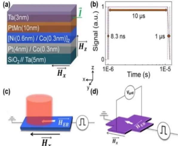
The system SiO2 // Ta (5 nm)/Pt (4 nm)/Co (0.3 nm)/[Ni (0.6 nm)/Co (0.3 nm)]2/PtMn (10 nm)/Ta (3 nm) studied is sketched in Fig. 1(a). By working with an ultrahigh-vacuum magnetron sputtering system, the PtMn/[Co/Ni]2 system has been deposited on thermally oxidized Si substrates without any magnetic sources according to the corresponding order: substrate // Ta (5 nm) / Pt (4 nm) / Co (0.3 nm) / [Ni (0.6 nm)/Co (0.3 nm)]2 / PtMn (10 nm) / Ta (3 nm). In particular, the bottom and top Ta layers have been used as adhesion and capping layers
FIG. 1. System structure and description of experimental
set-ups to measure SOT Switching. (a) Sketch of a SiO2 // Ta (5) / Pt (4) / Co(0.3) / [Ni (0.6) / Co (0.3)]2 / PtMn (10) / Ta (3) sample. (b) Current pulse profile used for SOT measurements. (c) Sketch of the experimental set-up to measure the SOT switching curves with P-MOKE configuration in a single-wire (5μm × 10μm). (d) Sketch of the experimental set-up to measure the Anomalous Hall Effect while injecting current in Hall cross (5 or 10μm x 10μm).
respectively. By using a Vibrating Sample Magnetometer (VSM), we investigated the most
suitable ferromagnet for our study and we confirmed that sheet-films involving PtMn exhibit the co-existence of Perpendicular Magnetic Anisotropy (PMA) and out-of-plane exchange bias. Once we managed to get the magnetic properties, the samples have been patterned into a Hall cross (5 µm or 10 µm by 10 µm) and/or into a bar (5 µm by 10 µm) by photolithography, magnetron sputtering and liftoff process. The same method has been used to set up the Ta(10 nm)/Pt(100 nm) electrodes in a second round of patterning.
III. RESULTS AND DISCUSSIONS A. Magnetic Properties
The magnetic properties of the sample were obtained by measuring its magnetisation as a function of the applied field with a VSM with different annealing procedures as shown in Fig. 2. Fig. 2(a)
and Fig. 2(b) present the hysteresis loops obtained on the as-grown sample for field applied perpendicular to the film plane and in-plane respectively whereas Fig. 2(c) and Fig. 2(d) show the hysteresis loops obtained after the double annealing procedure. The sample is heated at 583K then a magnetic field of 0.9T is applied along the direction perpendicular to the film plane (z axis) during the first 25 minutes and it is then applied along an in-plane direction (x axis) during the last 35 minutes before cooling down to room temperature. This provides a significant hysteresis loop shift both in the in-plane and the out-of-plane directions without damaging the PMA, i.e. maintaining nice square loops.
FIG. 2. Normalized magnetisation M/Ms as a function of the applied magnetic field. (a) As-deposited structure with the field applied perpendicular to the plane. (b) As-deposited structure with the field applied in the plane. (c) After annealing at 583K under 0.9T with the field applied perpendicular to the plane. (d) After annealing at 583K under 0.9T with the field applied in the plane.
Out-of-plane VSM measurements for annealed films exhibit square loops with a coercive field HC = 22mT and an out-of-plane exchange bias of 9mT. In addition, in-plane measurements show an in-plane
exchange bias of 20mT. The saturation magnetisation, for annealed films, reaches 0.927MA.m-1 with an anisotropy field of 500mT (5 000Oe), that is to say an effective magnetic anisotropy Keff = 0.23MJ.m-3.
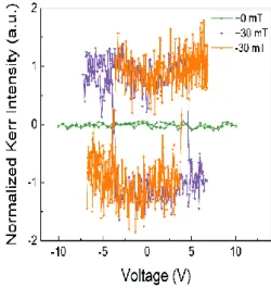
It should me mentioned that for a single step annealing at 583K under a field of 0.9T along the out-of-plane direction (z axis) during 60 minutes, no in-plane exchange bias is induced as shown on Fig. 3(a). Then, we performed Magneto Optical Kerr Effect (MOKE) measurements in polar configuration using the experimental set-up described in Fig. 1(c)
to get SOT switching curves on single-wire annealed only in the direction perpendicular to the plane to demonstrate that no zero field SOT switching is observed as shown on Fig. 4. On the other hand, if the annealing is performed with in-plane field only, no strong PMA is observed as shown inFig. 3(b).
B. Anomalous Hall Effect measurements
We performed Anomalous Hall Effect (AHE) measurements using the experimental set-up described in Fig. 1(d) to get SOT switching curves on Hall-crosses for both as-deposited and annealed systems. We applied pulse current starting from - 60mA to + 60mA (with a pulse profile corresponding to Fig. 1(b)) under a permanent in-plane magnetic field ranging from -30mT to +30mT. Fig. 5(a,c)
shows SOT loops for double annealed devices. The polarity switching occurs at HX,SWITCH = - 1.5mT for annealed devices due to the symmetry breaking. However, we demonstrated (see Fig. 5(b,d)) a polarity switching at HX,SWITCH = 0mT for non-biased
FIG. 3. Normalized magnetisation M/Ms as a function of the magnetic field applied in-plane and out-of-plane. (a) Sample after out-of plane annealing only. (b) Sample after in-plane annealing only.
devices. Note that the full current switching is observed only for applied field showing an absolute value larger than 10mT.
The amplitude of the AHE voltage variation generated by the SOT magnetisation switching decreases as the field reaches the polarity switching field (HX,SWITCH). In the case of the as-deposited sample at zero applied field HX = 0mT, the critical current tends to diverge and no switching can be observed since the switching voltage amplitude tends to zero. However, a significant switching voltage variation is observed under zero applied magnetic field after a double annealing procedure for a moderate current. Moreover, the Hall voltage versus current remains a square loop.
The critical switching current IC is plotted as a function of the in-plane field HX in Fig. 6. For the as-deposited sample the evolution of the critical current is symmetric i.e. similar behaviour is observed for positive and negative in-plane field. In the case of double annealed sample the evolution is asymmetric. In first approximation the IC versus HX is now centred around HX,SWITCH = - 1.5mT.
IV. CONCLUSION
In conclusion, we have demonstrated that using a double annealing procedure which consists in annealing the sample with a perpendicular to the plane followed by an in-plane applied magnetic field, we can combine a zero field SOT switching and a sharp out-of-planeswitching. Indeed this procedure induces both an in-plane and out-of-plane exchange bias phenomena which allows an in-plane symmetry breaking needed for the SOT switching but also maintains perpendicular magnetisation resulting in square Hall voltage versus current hysteresis loops. This procedure can be implemented to improve the design of future spintronics devices such as SOT-MRAM.
FIG. 4. Normalized Kerr intensity as a function of the applied
FIG. 5. Normalized VAHE as a function of injected current - IC for a SiO2 // Ta (5) / Pt (4) / Co(0.3) / [Ni (0.6) / Co (0.3)]2 / PtMn (10) / Ta (3) sample. (a), (c) As-deposited sample. (b), (d) Sample after double annealing procedure. (a) For various in-plane fields ranging from +30 mT to -1.5 mT leading to one type of SOT switching polarity. (b) For various in-plane fields ranging from +30 mT to 0 mT leading to one type of SOT switching polarity. (c) For various in-plane fields ranging from -1.5 mT to -30 mT leading to the other type of SOT switching polarity. (d) For various in-plane fields ranging from 0 mT to -30 mT leading to the other type of SOT switching polarity.
FIG. 6. Critical current as a function of the in-plane applied field
HX for the SiO2 // Ta (5) / Pt (4) / Co(0.3) / [Ni (0.6) / Co (0.3)]2 / PtMn (10) / Ta (3) sample as-deposited (red square) and after annealing following the procedure described in the text (blue circles).
ACKNOWLEDGMENTS
This work was supported partly by the French PIA project “Lorraine Université d’Excellence”, reference ANR-15-IDEX-04-LUE, by the “FEDER-FSE Lorraine et Massif Vosges 2014-2020”, a European Union Program. Maxime Verges is supported by a Cifre PhD grant from Vinci Technologies.
DATA AVAILIBILITY
The data that support the findings of this study are available from the corresponding author upon reasonable request
.
REFERENCES
1
M. D. Stiles, and A. Zangwill, Phys. Rev. B 66,
014407 (2002). 2
W. S. Zhao, Y. Zhang, T. Devolder, J.O. Klein, D. Ravelosona, C. Chappert, and P. Mazoyer,
Microelectronics Reliability 52, 1848 (2012).
3
H. Sato, H. Honjo, T. Watanabe, M. Niwa, H. Koike, S. Miura, T. Saito, H. Inoue, T. Nasuno, T. Tanigawa, Y. Noguchi, T. Yoshiduka, M. Yashiduka, M. Yasuhira, S. Ikeda, S.-Y. Kang, T. Kubo, K. Yamashita, Y. Yagi, R. Tamura, and T. Endoh,
IEDM Tech. Dig., 608 (2018). 4
I. M. Miron, G. Gaudin, S. Auffret, B. Rodmacq, A. Schuhl, S. Pizzini, and J. Vogel, and P. Gambardella, Nat. Mater. 9, 230 (2010).
5
L. Liu, O. J. Lee, T. J. Gudmundsen, D. C. Ralph, and R. A. Buhrman, Phys. Rev. Lett. 109, 096602
(2012). 6
K. Garello, I. M. Miron, C. O. Avci, F. Freimuth, Y. Mokrousov, S. Blügel, S. Auffret, O. Boulle, G. Gaudin and P. G., Nat. Mater. 11, 372 (2012).
7
Y. K. Kato, R. C. Myers, A. C. Gossard, and D. D. Awschalom, Science 306, 1910 (2004).
8
A. Brataas, A. D. Kent, and H. Ohno, Nat. Nanotech. 8, 587 (2013).
9
G. Yu, P. Upadhyaya, Y. Fan, J. G. Alzate, W. Jiang, K. L. Wong, S. Takei, S. A. Bender, L. Chang, Y. Jiang, M. Lang, J. Tang, Y. Wang, Y. Tserkovnyak, P. K. Amiri, and K. L. Wang, Nat. Nanotech. 9, 548 (2014).
10
W. H. Meiklejohn, and C. P. Bean, Phys. Rev.
102, 1413 (1956).
11
J. Nogués, and I. K. Schuller, J. Magn. Magn. Mater. 192, 203 (1999).
12
S. Fukami, C. Zhang, S. DuttaGupta, A. Kurenkov, and H. Ohno, Nat. Mater. 15, 535 (2016). 13
W. A. Borders, S. Fukami, and H. Ohno, IEEE Trans. Magn. 53, 535 (2017).
14
A. Kurenkov, C. Zhang, S. DuttaGupta, S. Fukami, and H. Ohno, Appl. Phys. Lett. 110, 092410 (2017).
15
E. Krén, G. Kádár, L. Pál, J. Sólyom, P. Szabó and T. Tarnóczi, Phys. Rev. 171, 574 (1968). 16
V. Baltz, A. Manchon, M. Tsoi, T. Moriyama, T. Ono, and Y. Tserkovnyak, Rev. Mod. Phys. 90, 015005 (2018).
17
Y. Ou, S. Shi, D. C. Ralph, and R. A. Buhrman,
Phys. Rev. B 93, 220405 (2016).
18
W. Zhang, M. B. Jungfleisch, W. Jiang, J. E. Pearson, A. Hoffmann, F. Freimuth, and Y. Mokrousov, Phys. Rev. Lett. 113, 196602 (2014). 19J. Železný, P. Wadley, K. Olejník, A. Hoffmann, and H. Ohno, Nat. Phys. 14, 220 (2018).
20
M. Saito, N. Hasegawa, F. Koike, H. Seki, and T. Kuriyama, J. Appl. Phys. 85, 4928 (1999).
21
M. L. Schneider, M. R. Pufall, W. H. Rippard, and S. E. Russek, Appl. Phys. Lett. 90, 092504 (2007).
22
J. P. Nozières, S. Jaren, Y. B. Zhang, A. Zeltser, K. Pentek, and V. S. Speriosu, J. Appl. Phys. 87, 3920 (2000).
23
P. F. Ladwig, Y. A. Chang, E. S. Linville, A. Morrone, J. Gao, B. B. Pant, A. E. Schultz, and S. Mao, J. Appl. Phys. 94, 979 (2003).
24
A. Maesaka, S. Ishii, and A. Okabe, J. Appl. Phys.
88, 3982 (2000).
25
Y.-W. Oh, S.-H. C. Baek, Y. M. Kim, H.-Y. Lee, K.-D. Lee, C.-G. Yang, E.-S. Park, K.-S. Lee, K.-W. Kim, G. Go, J.-R. Jeong, B.-C. Min, H.-W. Lee, K.-J. Lee, and B.-G. Park, Nat. Nanotech. 11, 878 (2016).
26
A. van den Brink, G. Vermijs, A. Solignac, J. Koo, J. T. Kohlhepp, H. J. M. Swagten, and B. Koopmans, Nat. Comm. 7, 10854 (2016).
27
P.-H. Lin, B.-Y. Yang, M.-H. Tsai, P.-C. Chen, K.-F. Huang, H.-H. Lin, and C.-H. Lai, Nat. Mater. 18,
335 (2019).
![FIG. 5. Normalized V AHE as a function of injected current - I C for a SiO2 // Ta (5) / Pt (4) / Co(0.3) / [Ni (0.6) / Co (0.3)] 2 / PtMn (10) / Ta (3) sample](https://thumb-eu.123doks.com/thumbv2/123doknet/14439573.516662/5.892.141.753.112.543/fig-normalized-ahe-function-injected-current-ptmn-sample.webp)
