HAL Id: hal-01291713
https://hal.archives-ouvertes.fr/hal-01291713
Submitted on 21 Mar 2016
HAL is a multi-disciplinary open access
archive for the deposit and dissemination of
sci-entific research documents, whether they are
pub-lished or not. The documents may come from
teaching and research institutions in France or
abroad, or from public or private research centers.
L’archive ouverte pluridisciplinaire HAL, est
destinée au dépôt et à la diffusion de documents
scientifiques de niveau recherche, publiés ou non,
émanant des établissements d’enseignement et de
recherche français ou étrangers, des laboratoires
publics ou privés.
Nucleation, imaging and motion of magnetic domain
walls in cylindrical nanowires
Sandrine da Col, Ségolène Jamet, M Staňo, B. Trapp, S. Le Denmat, L
Cagnon, J.-C. Toussaint, Olivier Fruchart
To cite this version:
Sandrine da Col, Ségolène Jamet, M Staňo, B. Trapp, S. Le Denmat, et al.. Nucleation, imaging
and motion of magnetic domain walls in cylindrical nanowires. Applied Physics Letters, American
Institute of Physics, 2016, 109 (6), pp.062406. �10.1063/1.4961058�. �hal-01291713�
S. Da Col,1, 2 S. Jamet,1, 2 M. Staňo,1, 2 B. Trapp,1, 2 S. Le Denmat,1, 2 L. Cagnon,1, 2 J. C. Toussaint,1, 2 and O. Fruchart1, 2, 3, 4,∗
1Univ. Grenoble Alpes, F-38000 Grenoble, France 2
CNRS, Inst NEEL, F-38000 Grenoble, France 3
CNRS, SPINTEC, F-38000 Grenoble, France 4CEA, INAC-SPINTEC, F-38000 Grenoble, France
(Dated: March 21, 2016)
We report several procedures for the robust nucleation of magnetic domain walls in cylindrical permalloy nanowires. Specific features of the magnetic force microscopy contrast of such soft wires are discussed, with a view to avoid the misinterpretation of the magnetization states. The domain walls could be moved under quasistatic magnetic fields in the range 0.1−10 mT.
I. INTRODUCTION
The motion of magnetic domain walls (DWs) in one-dimensional structures has been a subject of increasing interest over the past two decades1. Such structures
pro-vide a model playground to investigate DW motion un-der magnetic field or spin-polarized current. They have been proposed to serve as a basis for logic2 or memory schemes3. So far, fundamental physics and demonstra-tors made use of flat strips patterned out of thin films, for ease of fabrication and inspection. One may also con-sider the cylindrical geometry, which we name wire in the following. Wires can be fabricated with bottom-up techniques by electroplating magnetic metals in insulat-ing templates displayinsulat-ing cylindrical pores4. Dense arrays of vertical wires would be the natural geometry to imple-ment the proposal of a 3D magnetic race-track memory3.
For wires, theory and simulations5–7 suggested the
exis-tence of two types of DWs: the transverse wall and the Bloch-point wall. The features of their motion under field5–7 or current8 were predicted to be even more
sim-ple than in strips, mostly precessional in its azimuth in the former case, and purely translational for the second case with speed around 1 km/s, and absence of Walker instabilities.
To search for this physics, there are three requirements: nucleate DWs in a controlled fashion; image them with a simple technique; the material is sufficiently soft so that DWs may be moved under moderate field. These three steps are reported in this manuscript.
II. TECHNIQUES
As regards synthesis, we start from insulating porous templates obtained by anodization of aluminum in oxalic acid4. Constant voltage leads to straight pores, while for
some wires bursts at higher voltage have been used to cre-ate local protrusions, i.e. with larger diameter. Fe20Ni80
wires were then obtained by electroplating at −1.0 V ver-sus saturated calomel electrode in an electrolyte contain-ing 0.5 M Ni2+ and 0.02 M Fe2+ with pH = 3. Finally, the template is dissolved in 2 M NaOH , the wires are rinsed several times in water and isopropanol before a drop of solution is left to dry on a supporting surface for further inspection.
Magnetic force microscopy (MFM) was performed with an NT-MDT NTegra Aura instrument. We used Olym-pus AC240TS cantilevers (stiffness ≈ 2 N/m), custom-coated with Co80Cr20of thickness from 3 to 10 nm.
Imag-ing was performed in air with the ac two-pass technique, monitoring the phase during the lifted pass. The peak-to-peak amplitude of the tip is circa 40 nm. The lift height is in the range 20−50 nm. Micromagnetic simulations were performed with the home-made finite-elements mi-cromagnetic code FeeLLGood9. MFM contrast was
esti-mated as the map of the second vertical derivative of the vertical component of the simulated stray field.
III. NUCLEATION
Several strategies have been demonstrated to prepare DWs in a controlled manner in patterned strips, such as injection from a large pad10 or nucleation at the bends
of curved wires using a large transverse field11. The
lesser versatility of design in bottom-up systems makes the preparation of DWs an issue specific to wires.
In a long and narrow wire made of a soft magnetic ma-terial, uniform magnetization is the ground state. A non-uniform distribution of magnetization may develop lo-cally at either end such as "C" or curling end domains5,6.
These eventually lead to nucleation of a DW at a value of magnetic field Hn lower than the average transverse
demagnetizing field, the latter being close to Ms/2.
Let-ting aside thermal activation, the nucleation field is de-termined by the wire diameter normalized to the dipolar exchange length ∆d = p2A/(µ0Ms2), with A the
ex-change stiffness. The value of Hn decreases for
increas-ing diameter12. H
nmay equal or exceed 100 mT for
sub-50 nm-diameter wires. Thus, unless the material suffers from very large local pinning (in which case we would
2
disregard it to investigate DW motion)13, the nucleation of a DW is immediately followed by its very fast propa-gation along the wire and annihilation at the other end, leaving again the wire in a single-domain state.
One possibility to nucleate and keep a DW at rema-nence, is to align magnetization exactly perpendicular to the wire axis using a large external field, before go-ing back to remanence. An oscillatory demagnetization along such a direction may be used as well. One or sev-eral DWs may be nucleated at a location away from the ends of the wire, thanks to local imperfections or ther-mal fluctuations. This has been employed successfully by others, and made possible the first observation of a transverse wall in a wire, using electron holography14.
However, our experience is that the alignement of the applied field is critical. Indeed, magnetization is already close to parallel to the wire axis under a transverse field back to ≈ 100 mT. Thus, a misalignment of less than one degree is enough to move a created DW towards an end, thus to annihilate it, if the propagation field is of the order of ≈ 1 mT. It is desirable to have more robust procedures for nucleation of DWs. We describe below two such procedures that we implemented successfully.
The first procedure is to modulate the wire diameter along its length. Indeed, as the DW energy increases with the diameter7,15, protrusions and constrictions are
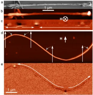
expected to act as energy barriers and wells, respectively. The modulation may induce sufficient pinning so that demagnetization with a transverse magnetic field as de-scribed previously, is less critical with the alignment. This procedure is illustrated on Fig.1(a-c), and was used by us to evidence again transverse walls and also for the first time Bloch-point walls by photo-emission electron microscopy17. Note however that, as the resulting
pin-ning field is expected to be lower than the longitudinal nucleation field Hn, a magnetization process with a
mag-netic field applied along the wire axis still consists of nucleation-propagation-annihilation and cannot lead to a multi-domain wire16.
The second procedure consists in making use of a curved shape, saturating magnetization across the ra-dius, before coming back to remanence. This procedure is straightforward to implement in strips, designed at will by lithography11. As for cylindrical wires, it sometimes
happens that a wire is bent during the dispersion proce-dure. It is possible to drastically increase the yield by first aligning the wires along a given in-plane direction thanks to an applied magnetic field, followed by drying the solution with a blow of air along the in-plane direction transverse to the field. Fig.1(d,e) shows a wire prepared this way, where head-to-head and tail-to-tail DWs could be nucleated at two opposite bends.
IV. IMAGING
DW motion cannot be tracked with giant magneto-resistance like for strips18, as a current-in-plane
spin-d e H b c 1 μm a 1 μm H
Fig. 1: (a) Scanning electron, (b) AFM (c) MFM of a wire with diameter 80 nm displaying local protrusions with diam-eter 150 nm, and demagnetized with a large field applied per-pendicular to the plane. (d,e) Atomic and magnetic force mi-croscopy of a bent wire with diameter 60 nm, prepared with an in-plane saturating field.
valve structure is not easy to implement for a wire. Mag-netic microscopy is therefore expected to play a key role, with MFM being a tool of choice, as an in-lab technique requiring no special sample preparation. However, MFM has known issues, such as tip-sample interaction and im-age analysis. We discuss below the specific aspects of these in the case of wires.
Tip-sample interaction must be small enough to avoid dragging DWs during imaging, as low-pinning materials are targeted. The stray field of an MFM tip extends over a length scale similar to the radius of curvature of its apex, which is a few tens of nanometers. Thus, for the wires considered here, the interaction issue is a priori stronger than for flats strips of width several hundreds of nanometers, because the entire DW is under the influence of the stray field. The present MFM images were made using tips with magnetic coating in the range 3−10 nm, which was found to avoid dragging DWs in wires with pinning field as low as 1 mT. This comes at the expense of a lower MFM signal, with a phase shift much smaller than a degree. On the other hand, such low-moment tips avoid most of the mutual contrast expected to scale like the square of the tip moment19, thus giving a more
faithful map of the stray field emanating from the sample. As regards contrast analysis, in most instruments the tip oscillates essentially along the normal to the sample, and the tip magnetization is also along the same direc-tion. Thus, it is assumed that MFM reflects a vertical derivative of the vertical component of the stray field, it-self related to the neighboring sample magnetic charges.
Thus, DWs are expected to display a monopolar con-trast, dark or light depending on their polarity. To first approximation this is the case in Fig.1(c,e). As already noticed, modulations of diameter16 as well as roughness
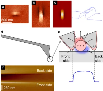
or structural / anisotropy fluctuations20also induce a lo-cal contrast, with monopolar and dipolar feature along the wire direction, respectively. However, a closer look reveals also a transverse dark/light dipolar contrast per-pendicular to the axis at DWs, diameter modulations and wire ends (Fig. 1, and zoom on a DW on Fig. 2a). Ro-tating the wire by 90◦ so that the cantilever is oriented along the wire axis, yields a side contrast again opposite to the contrast on wire, however now symmetric with respect to the wire axis (Fig. 2b). The ground for the contrast is the following. When the magnetic center of mass of the tip is below the mid-height plane of the wire, the vertical component of stray field is opposite to that above the wire (Fig. 2e). The asymmetric contrast oc-curring for wires horizontal in the images (i.e. transverse to the cantilever direction) stems from the tilt of the tip apex with respect to the sample normal, providing less access to the back side of the wire (Fig. 2e). The angle results from the tilt of the cantilever from the sample plane, combined with the tilt of the tip axis with respect to the normal to the cantilever for the Olympus AC se-ries (Fig.2d). Note that the former tilt, which induces a non-vertical direction of oscillation, may also play a role in the front- versus back side contrast, weighing spatial derivatives of the stray field along two directions21,22.
Fig.2b is reasonably reproduced by the simulation of MFM contrast of a Bloch-point wall (Fig. 2c), although not taking into account the above-mentioned tilts. Note also that it is not granted that experimentally a Bloch-point wall may be distinguished from a transverse wall, due to the finite spatial resolution. Anyway, it would be wrong to interpret Fig.2a as a signature for a trans-verse wall; it is an instrumental feature, which has the strongest signature for large-diameter wires as in Fig.1c compared to Fig.1e, and more generally for small thick-ness of tip coating, small oscillation amplitude and small lift height (Fig.2f).
V. PROPAGATION
The wires have been subjected to a quasistatic mag-netic field during typically 1 s. The MFM tip is parked a few micrometers away from the imaging area during the pulse, so that no magnetic bias from the tip is acting on the wire. Imaging is then performed at remanence.
DWs could be moved in the two afore-mentioned cases: wires with either bends or modulations of diameter. In both cases there exists a distribution of pinning sites along the wire length. The distribution of pinning fields in a one-dimensional system due to statistical disorder, has been one of the earliest concepts to describe magne-tization reversal. Its general form is now known as the Becker-Kondorski model23,24. It has been detailed
re-b c a 500 nm + + + d e 250 nm f Front side Back side Front side Back side Front side e
Fig. 2: (a,b) MFM images of a domain wall in a wire with diameter 70 nm, with the cantilever perpendicular and par-allel to the wire axis, respectively. (c) Simulated ∂2H
z/∂z2, based on a Bloch-point wall. The side sketch shows the 10 nm-lift surface where the contrast is calculated, reflecting a con-ical shape for the tip, rounded with a radius of curvature 10 nm. The width at the base of the wire was set to 105 nm. (d) Schematic shape of the Olympus tips, and their tilt in our microscope. (e) Sketch for the stray field associated with mag-netic charges in a wire. The bottom part is the cross-section of the experimental topography associated with (f), with a true aspect ratio (f) Experimental single-line scan close to the end of a 140 nm-diameter wire, while varying the lift height from 20 to 200 nm from left to right (oscillation amplitude kept constant at 50 nm).
cently for wires, evaluating the impact of e.g. roughness and fluctuations of magnetocrystalline anisotropy25.
Examination of several wires reveals a broad distri-bution of wire- and location-dependent pinning fields, from below 0.1 mT to around 10 mT. No clear corre-lation was found with roughness, so that it may result from a material issue involving microstructure and/or strain. Note that such distributions are also a common feature for thin strips deposited by physical means such as sputtering, when investigated step by step by magnetic microscopy26.
Conclusion
We demonstrated two methods for the controlled nu-cleation of domain walls (DWs) in cylindrical wires, and highlighted specific features of MFM contrast for such wires. Motion of the DWs is demonstrated with pinning field strength in the range 0.1−10 mT. These values are similar to those in strips with in-plane or out-of-plane magnetization, in which the dynamics of DW motion was
4 -20.0 mT e +11.5 mT d +10.0 mT c +4.5 mT b a 1 μm
Fig. 3: (a-e) Successive steps of remagnetization of the wire shown in Fig.1c. The images are taken at remanence, each following a magnetic field with an increasing magnitude from top to bottom. Arrows depict the local direction of magneti-zation. Positive fields point to the right. In (d) and (e) DWs have moved across modulations of diameter.
already largely investigated. The route is therefore open to the experimental search of the peculiar features pre-dicted for DW dynamics in cylindrical wires.
Acknowledgements
We acknowledge helpful discussions with A. Wartelle (Institut NEEL) and A. Fernandez-Pacheco (Cavendish Laboratory). This project has received funding from the European Union Seventh Framework Programme (FP7/2007-2013) under grant agreement n◦309589 (M3d).
References
1 L. Thomas and S. S. P. Parkin, “Micromagnetism,” (Wi-ley, Chichester, England, 2007) Experiment, magnetism, transport, review Current induced domain-wall motion in magnetic nanowires, pp. 942–982.
2
D. A. Allwood, G. Xiong, M. D. Cooke, C. C.Faulkner, D. Atkinson, N. Vernier, and R. P. Cowburn, Science 296, 2003 (2002).
3 S. S. P. Parkin, M. Hayashi, and L. Thomas, Science 320, 190 (2008).
4
C. T. Sousa, D. C. Leitao, M. P. Proenca, J. Ventura, A. M. Pereira, and J. P. Araujo, Appl. Phys. Rev. 1, 031102 (2014), ISSN 1931-9401,http://dx.doi.org/10. 1063/1.4893546.
5 H. Forster, T. Schrefl, D. Suess, W. Scholz, V. Tsiantos, R. Dittrich, and J. Fidler, J. Appl. Phys. 91, 6914 (2002). 6
R. Hertel, J. Magn. Magn. Mater. 249, 251 (2002). 7 A. Thiaville and Y. Nakatani, “Spin dynamics in confined
magnetic structures iii,” (Springer, Berlin, 2006) Domain-wall dynamics in nanowires and nanostrips, pp. 161–206. 8 A. Thiaville and Y. Nakatani, “Nanomagnetism and
spin-tronics,” (Elsevier, 2009) Micromagnetic simulation of do-main wall dynamics in nanostrips.
9
F. Alouges, E. Kritsikis, J. Steiner, and J.-C. Toussaint,
Numer. Math., 1(Feb 2014), ISSN 0945-3245,http://dx. doi.org/10.1007/s00211-014-0615-3.
10
K. Shigeto, T. Shinjo, and T. Ono, Appl. Phys. Lett. 75, 2815 (1999).
11
T. Taniyama, I. Nakatani, T. Namikawa, and Y. Yamazaki,
Phys. Rev. Lett. 82, 2780 (1999),http://link.aps.org/ doi/10.1103/PhysRevLett.82.2780.
12
H. Zeng, R. Skomski, L. Menon, Y. Liu, S. Bandyopadhyay, and D. J. Sellmyer, Phys. Rev. B 65, 134426 (2002). 13 Y. Henry, K. Ounadjela, L. Piraux, S. Dubois, J.-M.
George, and J.-L. Duvail, Europhys. J. D 20, 35 (2001). 14
N. Biziere, C. Gatel, R. Lassalle-Balier, M. C. Clochard, J. E. Wegrowe, and E. Snoeck, Nano Lett. 13, 2053 (2013).
15 S. Jamet, N. Rougemaille, J. C. Toussaint, and O. Fruchart, “Magnetic nano- and microwires: Design, syn-thesis, properties and applications,” (Woodhead, 2015) Head-to-head domain walls in one-dimensional nanostruc-tures: an extended phase diagram ranging from strips to cylindrical wires.
16
K. Pitzschel, J. Bachmann, S. Martens, J. M. Montero-Moreno, J. Kimling, G. Meier, J. Escrig, K. Nielsch, and D. Görlitz, J. Appl. Phys. 109, 033907 (2011).
17
S. Da Col, S. Jamet, N. Rougemaille, A. Locatelli, T. O. Mentes, B. S. Burgos, R. Afid, M. Darques, L. Cagnon, J. C. Toussaint, and O. Fruchart,Phys. Rev. B
89, 180405 (2014),http://link.aps.org/doi/10.1103/ PhysRevB.89.180405.
18
J. Grollier, P. Boulenc, V. Cros, A. Hamzic, A. Vaurès, A. Fert, and G. Faini, Appl. Phys. Lett. 83, 509 (2003). 19 D. W. Abraham and F. A. McDonald,Appl. Phys. Lett.
56, 1181 (1990). 20
O. Iglesias-Freire, C. Bran, E. Berganza, I. Mínguez-Bacho, C. Magén, M. Vázquez, and A. Asenjo, Nanotechnology 26, 395702 (2015).
21
D. Rugar, H. J. Mamin, P. Guethner, S. E. Lambert, J. E. Stern, I. MCFaydien, and T. Yogi, J. Appl. Phys. 68, 1169 (1990).
22
G. Ciuta, F. Dumas-Bouchiat, N. M. Dempsey, and O. Fruchart(2016),http://arxiv.org/abs/1510.09004. 23 R. Becker, Phys. ZS, 905(1932).
24
E. Kondorski, Phys. Z. Sowjetunion 11, 597 (1937). 25
A. A. Ivanov and V. A. Orlov, Phys. Sol. State 53, 12 (2011).
26
L. Serrano-Raman, A. Fernandez-Pacheco, M. R. Ibarra, D. Petit, R. P. Cowburn, T. Tyliszczak, and J. M. De Teresa, Europhys. J. D 86, 97 (Mar 2013), ISSN 1434-6036, http://dx.doi.org/10.1140/ epjb/e2013-30926-5.