HAL Id: hal-02196277
https://hal.archives-ouvertes.fr/hal-02196277
Submitted on 27 Jul 2019HAL is a multi-disciplinary open access
archive for the deposit and dissemination of sci-entific research documents, whether they are pub-lished or not. The documents may come from teaching and research institutions in France or abroad, or from public or private research centers.
L’archive ouverte pluridisciplinaire HAL, est destinée au dépôt et à la diffusion de documents scientifiques de niveau recherche, publiés ou non, émanant des établissements d’enseignement et de recherche français ou étrangers, des laboratoires publics ou privés.
Role of Impurities in Silicon Solidification and Electrical
Properties Studied by Complementary in Situ and Ex
Situ Methods
Hadjer Ouaddah, Isabelle Perichaud, Damien Barakel, Olivier Palais, Marisa
Di Sabatino, Guillaume Reinhart, Gabrielle Regula, Nathalie Mangelinck-Noël
To cite this version:
Hadjer Ouaddah, Isabelle Perichaud, Damien Barakel, Olivier Palais, Marisa Di Sabatino, et al.. Role of Impurities in Silicon Solidification and Electrical Properties Studied by Complementary in Situ and Ex Situ Methods. physica status solidi (a), Wiley, 2019, 1900298, pp.1-10. �10.1002/pssa.201900298�. �hal-02196277�
1 Role of impurities in silicon solidification and electrical properties studied by complementary in situ and ex situ methods
Hadjer Ouaddah, Isabelle Périchaud, Damien Barakel, Olivier Palais, Marisa Di Sabatino, Guillaume Reinhart, Gabrielle Regula, Nathalie Mangelinck-Noël*
Hadjer Ouaddah, Dr. Isabelle Périchaud, Dr. Damien Barakel, Prof. Olivier Palais, Dr. Guillaume Reinhart, Dr. Gabrielle Regula, Dr. Nathalie Mangelinck-Noël
Aix Marseille Univ, Université de Toulon, CNRS, IM2NP, Marseille, France nathalie.mangelinck@im2np.fr
Prof. Marisa Di Sabatino
NTNU, Department of Materials Science and Engineering, Trondheim, Norway
Keywords: Silicon, Photovoltaic, Growth defects, Impurities, Lifetime
Abstract:
All silicon (Si) ingot fabrication processes share challenges to control grain structure, defect and impurity contamination during the solidification step to improve the material properties. The final grain structure and inherent structural defects issued from the solidification step are responsible for the photovoltaic (PV) properties for a large part, all the more as they are often associated with impurity distribution. Impurities play a major role as they not only can modify the development of the grain structure formation but interact as well with structural defects creating regions of deleterious minority carrier lifetime recombination. Samples containing different levels of impurities and solidified with different processes were selected and analyzed as-grown or observed by X-ray imaging during re-solidification from as-grown seeds. The growth features and relative crystallographic orientation of neighbor grains were characterized. Moreover, minority carrier lifetime measurements were performed and correlated to the growth features. The complementarity of the different techniques allows improving the understanding of phenomena at stake during the formation of grains and twins, the effect of impurities and their impact on photovoltaic properties. The results show the significant influence of light and metallic impurities such as copper on the grain structure and on the electrical properties.
2 1. Introduction
The development of solar photovoltaic (PV) electricity requires significant advances in research and development to answer to the constantly renewed societal demand for higher conversion efficiency and lower costs. Silicon technology has clear advantages over other technologies: advantages such as the good availability of basic material (silica), the relatively high energy conversion efficiency and the good stability of the solar cells resulting in an expected lifetime of about 30 years. Moreover, silicon is a well-established technology still representing about 90% of the world photovoltaic market.[1] Existing fabrication processes produce either mono-crystalline or multi-crystalline ingots. Recently, alternative methods have been proposed to improve the quality of the Si ingots.[2, 3] However, for all Si ingot fabrication processes, the grain structure, defect and impurity contamination control during the solidification step remains a major challenge to improve the material properties. The final grain structure and associated defects (grain boundaries and dislocations) issued from the solidification step are responsible for PV properties for a large part.[4] In this context, impurities play a major role as they not only modify grain nucleation and competition during solidification[5, 6] but interact as well with structural defects.[7] The nucleation of new grains during growth can happen
either on the crucible walls or on precipitates or impurities in the molten silicon. Moreover, in a material contaminated with impurities, segregation along grain boundaries and extended defects (dislocations[7-10], twins) can be detrimental for the cell conversion efficiency. On the one hand, grain boundaries can have a positive effect by purifying the grain core from impurities by segregation and trapping. On the other hand, the impurities accumulated at the grain boundaries may be responsible for the increase of the defect recombination strength.[11] Within this context, the grain crystallographic orientation deriving directly from nucleation and grain competition during growth [12, 13] is of particular importance. Indeed, grain boundaries can have different propensity to segregation, mechanical, and electrical characteristics according to their crystalline quality and to the presence of dangling bonds.[14, 15] Impurities in general, and light impurities such as carbon (C), oxygen (O), and
3 fabricate silicon for PV applications. The furnace environment (heaters, graphite plate…) and crucible are often responsible for most of the light impurity contamination [16, 17] and in some cases for metallic impurity contamination.[18-21] In addition, impurities can be found in the starting feedstock used for PV applications.
The control of the final crystalline grain structure, the decrease of the structural defect density, and the control of the impurity concentration and segregation during crystal growth are objectives that can only be attained with a thorough understanding of the crystallisation mechanisms [22-24] and of the complex interaction between growth defects and impurities. Within this context, the objective of the present work is to correlate the growth mechanisms and defects to the electrical properties in presence of different impurity concentrations.
2. Experimental
Sample origin
The samples selected in the present work were obtained by different solidification processes. The selection of these samples aimed at encompassing representative solidification features and different levels of contamination.
Three samples (F1-F3) were cut from a zone melting ingot.[25] This process although costly allows producing mono-crystalline samples with a very low level of contamination (Sample type F in Table 1). Sample Cz was cut from a Czockralski ingot. This process allows producing mono-crystalline samples with a low level of contamination except for oxygen coming from the used quartz crucible (Sample Cz in Table 1). Another sample (Sample P in Table 1) was obtained from an ingot processed with the conventional multi-crystalline Si method [26] and corresponds to a conventional solar grade mc-Si quality. Samples C1, C2, V and J in Table 1 were processed using the cold crucible continuous casting solidification technique. This technique allows the growth of multi-crystalline silicon ingots without contact with the crucible walls thus reducing stresses and contamination by the crucible. Copper inductors are crossed by an alternating current and produce a magnetic field [27, 28], which
4 inductors. This process was previously used for instance by the French company EMIX. The main additional advantage of this technique, apart from the low level of contamination due to the absence of crucible, is that it provides the possibility to carry out continuous casting. In summary, this technique allows to increase the productivity and to decrease the impurity concentration in the ingots mainly in carbon and oxygen.[29] However, the use of the Cu inductors is at the origin of
contamination by Cu as can be seen in Table 1.
The concentrations of the main elements measured in the different samples used for the experiments are gathered in Table 1. It refers to the as grown samples following the processes described in the above paragraph. It is worth noticing that only the detectable impurities are provided in the following table implying that the other metallic impurity concentrations are below the detection limit. As a consequence, Cu contamination is the sole significant metallic impurity contamination for samples V, C1 and C2.
Table 1. Concentrations of the detectable impurities in the as grown samples. DL is the detection limit: 1 ppbw and 1 ppm for GDMS (Glow Discharge Mass Spectroscopy)[30] and IGA (Instrumental
Gas Analysis), respectively.
In situ X-ray radiography during the solidification Sample type F (F1 to F3) Cz[31] V J P C1 C2 Oxygen concentration (at.cm-3) < 1015 5-10 1017 5 1015 SIMS 8.6 1015 SIMS 3.7 1017 IGA 3.3 1017 FTIR 3.7 1016 SIMS 4.3 1016 SIMS Carbon concentration (at.cm-3) < 1015 5-10 1015 2.5 1016 SIMS 3.6 1017 SIMS < DL IGA 1.3 1017 FTIR 3.15 1017 SIMS 4.2 1017 SIMS Copper concentration (at.cm-3) - - 6.2 1015 GDMS < DL GDMS < DL GDMS 3.9 1015 GDMS 2.2 1017 GDMS
5 Some of the samples were characterised directly after the above described processes. Additionally, some parts of the ingots were used as seeds for solidification studies in the IM2NP device named GaTSBI (Growth at high Temperature observed by Synchrotron Beam Imaging), which allows in situ X-ray imaging during solidification. The samples were directionally solidified in the furnace that consists in two independent heating elements, constituted by two graphite heating resistors that can reach 1800°C under a vacuum of 10-6 mbar. The temperature is adjusted above and below the melting point in the top and bottom heating resistors, respectively. This creates a temperature gradient and allows the control of the position of the solid-liquid interface. In the present work, solidification was carried out by cooling down the heating element. The solid seed-liquid interface was first positioned in the field of view for X-ray imaging in between the two heating elements and a cooling rate was applied on both heating zones to trigger the solidification. The sample was fixed and the solid-liquid interface moved in the laboratory reference frame.
The melting and solidification is characterized in situ inside the GaTSBI device with synchrotron radiation X-ray radiography imaging technique at the ESRF (European Synchrotron Radiation Facility) in Grenoble, France. During solidification, the sample is illuminated by a polychromatic X-ray beam. Then, the transmitted polychromatic beam is monochromatized by a post-monochromator and recorded with a specific X-ray camera. In this mode, the image contrast is due to absorption differences. However, it is worth noticing that in the case of a pure material such as silicon, the density difference between the solid (2.33 g.𝑐𝑐𝑐𝑐−3) and the liquid (2.56 g. 𝑐𝑐𝑐𝑐−3) creates a small X-ray absorption difference. For this reason, image processing by image division is performed to reveal the solidification front. Radiography X-ray imaging brings information on morphology and growth kinetics of the solid-liquid interface. The experimental set-up, the method and the image processing details are described in more details elsewhere.[13, 32] During the experiments presented here, the images were recorded with an exposure time of 1 s with the ESRF FReLoN CCD camera equipped with an optics providing a resolution of about 12 µm.
6 To obtain quantitative and precise information about the crystallography of the grain structure, electron backscatter diffraction (EBSD) measurements are performed using a FEG-SEM JEOL JSM 7001F equipped with a HKL Nordlys camera using either a 15 µm or 7 µm lateral step size. At the end of the analysis, post-processing software is used to obtain several maps related to the crystallographic orientations. In the inverse pole maps, the color of each pixel corresponds to the crystallographic orientation of the {hkl} plane which is perpendicular to one of the axis of the reference frame. Coincidence site lattice maps (CSL) are reconstructed to evidence the boundaries with a special character. On top of the random angle grain boundaries, the main twin boundaries are highlighted in these maps namely: Σ3 〈111〉, Σ9 〈110〉, Σ27a 〈110〉, Σ27b 〈210〉 corresponding to rotations about 〈hkl〉 with an angle of (60 ± 8.66)°, (38.94 ± 5)°, (31.58 ± 2.89)° and (35.42 ± 2.89)° (colors red, blue, yellow and green in the figures), respectively. The character (symmetric or asymmetric) of the grain boundary and the orientation of the crystallographic planes of the adjacent grains are determined by the analysis of the stereographic projections of the appropriate crystallographic planes as done for example in our previous work.[23]
Micro Wave Phase Shift (µw-PS) minority carrier lifetime measurements
Minority carrier lifetime scan maps localize extended crystallographic defects that are electrically active. They can give an idea of the intensity of their recombination strength and allow comparing the relative recombination activity of different defects. In this work, minority carrier lifetime was determined by the microwave phase shift (μw-PS) technique.[33] In this method, microwaves are
driven towards the bottom surface of the sample by means of a microwave guide. Carrier generation is provided by a fiber-coupled laser diode with a wavelength of 942 nm, which is sine modulated in the range 0.5 - 70 kHz. The sinusoidal variation of the carrier density induces a sinusoidal variation of the reflectivity coefficient of the microwaves. The intensity of reflected microwaves are accurately measured by a lock-in amplifier. The phase shift between the modulated exciting light and the microwave can be mapped with a spatial resolution better than 50 μm, which leads to lifetime mapping with the same spatial resolution. This technique can be sensitive up to a contamination level
7 as low as 109 at.cm−3.[34] In order to determine the minority carrier lifetime from the measured phase shift, the sample thickness, the optical absorption coefficient at 942 nm, the minority carrier diffusion coefficient, the modulation frequency and the front and bottom surface recombination velocities have to be computed.
In this study, the optical absorption coefficient was taken equal to 535 cm−1 and a value of 30 cm2. s−1 was taken for the minority carrier diffusion coefficient. The modulation frequency was 6 kHz. A value of 6000 cm.s-1 was applied for the front and bottom surface recombination velocities.
This value corresponds to a cleaned raw silicon surface without passivation. 3. Results
3.1 Segregation and solid-liquid interface morphology
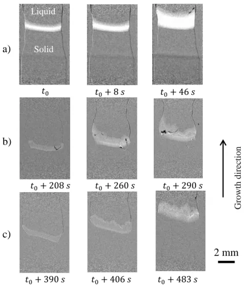
Figure 1 shows the radiography images obtained during the solidification of three samples: Cz, C1
and C2. The liquid and solid phases are in the upper and lower parts, respectively (see indications in
Figure 1.a). The image processing consists in division of the current image by a preceding one, hence the whiter contrast reveals the region which became solid in-between these two images and thus, reveals the solid-liquid interface.
Generally, when growing solar grade (e.g. sample P in Table 1) or higher quality samples (e.g. samples F and Cz in Table 1) in the GaTSBI furnace, no destabilization of the solid-liquid interface is observed by X-ray radiography during solidification as can be seen in Figure 1.a. The interface is smooth apart from grain boundary grooves and {111} facets.[35] The interface is also globally smooth in the case of samples containing light impurities (mainly C and O) as for example in samples J and P. Inversely, when studying the growth dynamics with X-ray radiography of C1 and C2 samples (Figure 1.b and 1.c) containing copper (Table 1), it appears that dendritic growth is observed under the same solidification conditions, even for a Cu concentration as low as 3.9 1015 at.cm-3 in sample C1.
8 Figure 1. Radiographs obtained on three kinds of samples at different instants during the solidification from seed, using the same cooling rate R = -4 K.min-1 applied at t0 with an applied
temperature gradient Gapp = 20 K.cm-1 a) Cz, b) C1 and c) C2 samples.
3.2 Grain nucleation and final grain structure
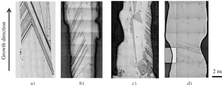
Figure 2 shows the final grain structure of samples F1, P, V and C2 after their growth inside the GaTSBI furnace.
Despite of the different growth conditions and level of impurities, all solidified samples exhibit the same kind of final grain structure, namely centimetric grain size and straight twin grain boundaries as can be seen in Figure 2. The level of Cu contamination is increasing from Figure 2.a to d. It means that Cu although modifying the interface microstructure has no significant effect on the final grain structure for these particular processing conditions.
b)
c)
a)
2 mm
𝑡𝑡0+ 208 𝑠𝑠 𝑡𝑡0 𝑡𝑡0+ 290 𝑠𝑠 𝑡𝑡0+ 260 𝑠𝑠 𝑡𝑡0+ 483 𝑠𝑠 𝑡𝑡0+ 406 𝑠𝑠 𝑡𝑡0 + 390 𝑠𝑠 𝑡𝑡0+ 8 𝑠𝑠 𝑡𝑡0+ 46 𝑠𝑠 G row th di re ct ion Solid Liquid9 Figure 2. Images of the final grain structure of samples grown by directional solidification in the GaTSBI furnace from seeds a) F1 (R = -1 K.min−1, Gapp = 37.5 K.cm−1), b) P (R = -2 K.min−1, Gapp
= 20 K.cm−1), c) V (R = -2 K.min−1, Gapp = 30 K.cm−1), and d) C2 (R = -0.2 K.min−1, Gapp = 20
K.cm−1).
Oppositely, there is a clear impact of C concentration on the grain structure. When C concentration increases, a larger amount of grains is observed at the end of growth. This effect is not only seen in the directional solidification experiments performed inside the GaTSBI furnace but as well in the industrial as-grown ingots with the industrial cold crucible continuous casting process.
Figure 3 shows the inverse pole figure in samples V (Figure 3.a) and J (Figure 3.b) both cut in as-grown ingots processed using the conventional industrial process conditions (Figure 3). It allows us characterizing the grain density as well as the different crystallographic orientations (grain orientation legend in Figure 3.c). The first qualitative visual assessment of Figure 3 indicates clearly that there is no preferential growth crystallographic orientation in both samples. Moreover, about twice more grains are present inside sample J compared to sample V for the same surface although the same growth process was used. The grains of sample V can extend up to several millimeters while more grains, having a smaller size of some hundreds of microns, are observed in sample J.
d) c) b) 2 mm G row th di re ct ion a)
10 Figure 3. Inverse pole figure (IPF) along the growth direction (left column) and transverse direction (right column) obtained by EBSD on samples directly issued from the industrial process: a) sample V, b) sample J, c) grain orientation legend.
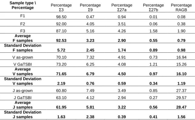
A quantitative assessment of the different grain boundary types was carried out from the EBSD measurements, the corresponding percentages of Σ3, Σ9, Σ27a, Σ27b twin boundaries and of random angle grain boundaries (RAGB) are gathered in Table 2. Regarding the samples type V and J, two kinds of samples were characterized by EBSD: as-grown samples characterized directly after the industrial process and others obtained after solidification in the GaTSBI furnace with an applied temperature gradient of 30 K/cm and a cooling rate of -2 K/min. Additionally, three solidification experiments were performed in the GaTSBI furnace with an applied temperature gradient of 30 K/cm and a cooling rate of -1 K/min (F1 to F3 in Table 2) using zone melting seeds (Type F in Table 1). Type F sample analysis gives consistent results. Σ3 twin boundaries are the most abundant in a large amount (92.53% in average) in all F-type samples. It is worth noting that this observation in pure seed samples was confirmed in several other in situ experiments.[13, 23] The amount of Σ3 twin boundaries
is decreasing for samples containing impurities in this order: V then J samples, which corresponds to an increasing level of C concentration (Table 1). Concomitantly, the amount of high order twin boundaries and of random angle grain boundaries increases. Moreover, it is worth noting that the values of the percentages obtained in as-grown and samples processed in the GaTSBI furnace are
{111} {110 } {100 } 2 mm c) b) a)
11 consistent and comparable with a standard deviation of 2.2% at maximum in samples V and J even though the processing conditions and ingot sizes were different.
Table 2. Percentage of the distribution of twin boundary types in F, V and J samples. RAGB corresponds to random angle grain boundaries. As-grown samples were processed using the cold crucible continuous casting. GaTSBI refers to sample processed using the GatSBI furnace with a temperature gradient of 30 K/cm and cooling rate of -2 K/min in both samples V and J.
Sample type \
Percentage Percentage Σ3 Percentage Σ9 Percentage Σ27a Percentage Σ27b Percentage
RAGB F1 98.50 0.47 0.94 0.01 0.08 F2 92.00 4.05 3.51 0.06 0.38 F3 87.10 5.16 4.26 1.58 1.90 Average F samples 92.53 3.23 2.90 0.55 0.79 Standard Deviation F samples 5.72 2.45 1.74 0.89 0.98 V as-grown 70.10 7.32 4.91 0.73 16.94 V GaTSBI 73.20 6.25 4.08 1.21 15.26 Average V samples 71.65 6.79 4.50 0.97 16.10 Standard Deviation V samples 2.19 0.76 0.59 0.34 1.19 J as-grown 60.80 7.49 3.49 0.85 27.37 J GaTSBI 63.10 4.12 2.94 0.27 29.57 Average J samples 61.95 5.81 3.22 0.56 28.47 Standard Deviation J samples 1.63 2.38 0.39 0.41 1.56
3. 3 Correlation with the electrical and photovoltaic properties
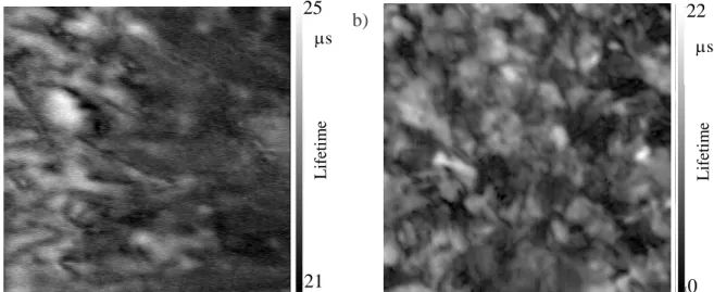
To correlate impurity concentrations and growth features with electrical properties, minority carrier lifetime maps were measured. Figure 4.a and 4.b show the lifetime maps obtained in the case of as-grown samples extracted directly from the industrial ingots of type V and J, respectively. It is important to note the scale difference between the two maps. For sample J (Figure 4.b), lifetime scale ranges from 0 to 22 µs, which means that the lifetime in the few white regions observed corresponds to 22 µs at maximum. Lifetime in sample V (Figure 4.a) is in average higher and more homogeneous;
12 with values ranging from 20 to 25 µs. Sample V map would appear all uniform if the same scale as the one for sample J was used. However, even in sample V map, some local lifetime variations exist and can only be highlighted with this scale. These local variations will be discussed in the following.
Figure 4. µw-PS minority carrier lifetime maps of samples a) V and b) J extracted from the industrial ingots.
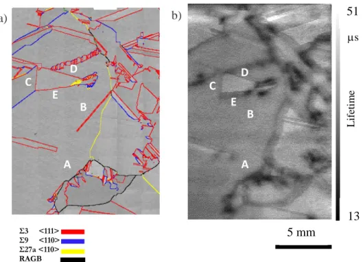
In Figure 5, a comparison is done between the coincidence site lattice map calculated from EBSD measurements (Figure 5.a) and the lifetime map (Figure 5.b) for sample P directly cut in a conventional mc-Si ingot.
Random angle grain boundaries (appearing in black in Figure 5.a) are clearly all active from the electrical point of view. Regions with a high number of small nucleating grains (e.g. A in Figure 5) are clearly active as well. The situation is different concerning Σ3 twin boundaries as some of them are active (C, D, E in Figure 5) and others are not active (B in Figure 5).
L if eti m e µs 25 2 mm b) a) 21 L if eti m e µs 22 0
13 Figure 5. Sample P: a) Coincidence Site Lattice (CSL) map. Red, blue, yellow, and black lines correspond to ∑3, ∑9, ∑27a and random angle grain boundaries (RAGB), respectively. b) µw-PS minority carrier lifetime map.
Figure 6. Sample V: a) Coincidence Site Lattice (CSL) map. Red, blue, yellow, and black lines correspond to ∑3, ∑9, ∑27a and random angle grain boundaries (RAGB), respectively. b) µw-PS minority carrier lifetime map.
Additionally, CSL and minority carrier lifetime maps of as-grown sample V (extracted from the industrial ingot) are shown in Figure 6. As in Figure 5, the random angle grain boundaries, appearing
5 mm Σ3 <111> Σ9 <110> Σ27a <110> RAGB A B C D A B C 13 51 E E D b) a) L if eti m e µs Σ3 <111> Σ9 <110> Σ27a <110> RAGB B 21 25 A C B A C B 2mm a) b) L if eti m e µs
14 in black in Figure 6.a, are active (e.g C in Figure 6). Moreover, as for sample P, some Σ3 grains boundaries are inactive whereas there is at least one unambiguously identified as an active one (A in Figure 6).
4. Discussion
The solid-liquid interface destabilization observed in Figure 1 is attributed to the presence of copper in samples C1, C2 (Table 1). As mentioned above, only the main impurities are shown in Table 1. Thus, Cu was the only detectable metallic impurity in samples C1 and C2. The interface destabilization is due to solute accumulation above the solid-liquid interface during growth. Indeed, the morphological destabilization is a mechanism of interface structuration during solidification to increase its exchange surface for better evacuation of the latent heat or excess solute. The Si-Cu phase diagram that can be found for example in[36] indicates that the partition ratio between Si and Cu is lower than 1 and is equal to 4. 10-4 [37]. The value of the partition ratio implies that Cu is rapidly accumulating above the solid-liquid interface as solidification progresses creating favorable conditions for morphological destabilization (dendrites in our case). Morphological destabilization has been widely studied in the literature; a review can be found here [38]. Details concerning these models are beyond the scope of the present study. Essentially, the destabilization due to constitutional undercooling is favored by a higher solute concentration, a lower temperature gradient and a higher growth rate. In directional solidification of alloys, an initially smooth growth front can become cellular or dendritic when the growth rate exceeds a threshold considering these parameters. A simple approach is given by the Tiller et al.[39] model and gives a critical growth rate for the destabilization of the solid-liquid interface:
𝑉𝑉𝐶𝐶 =(𝑘𝑘−1)𝑚𝑚𝐶𝐶𝑘𝑘𝐺𝐺𝐿𝐿𝐷𝐷𝐿𝐿0 (1)
where k is the partition coefficient of the impurity, GL is the liquid temperature gradient, DL the
diffusion coefficient of the impurity in the liquid, m the liquidus slope of the corresponding phase diagram and C0 the impurity nominal concentration. In the case of Cu impurity in Silicon, the partition
15 coefficient is 4. 10-4[37], the liquidus slope is estimated at 6.2 K.at%-1 from Olesinski et al.[40] and DL
≈ 10-8 m2.s-1.[41] It is worth noting that this approach can only give an order of magnitude of the
critical velocity for the interface destabilization. The average solid-liquid interface growth rates are measured during the experiments on three points at the solid-liquid interface before the dendritic destabilization: 56 µm.s-1 (standard deviation = 24 µm.s-1) for C1 and17 µm.s-1 (standard deviation = 6 µm.s-1) for C2. Then, the local temperature gradient at the solid-liquid interface is estimated according to the method described in Stamelou et al.[42]: 11 K.cm-1 and 39 K.cm-1 in samples C1 and C2, respectively. At last, equation (1) gives a critical velocity of 97 µm.s-1 and 6 µm.s-1 for samples
C1 and C2, respectively.
Concerning C2 sample, the growth rate is clearly above the estimated critical velocity which implies a destabilization of the interface as observed in Figure 1. The measured growth rate before the destabilization is lower than the critical velocity in sample C1. However, the order of magnitude and the standard deviation of the interface growth rate shows that the destabilization is also possible in this sample although less likely. Indeed, the maximum measured solid-liquid interface growth rate in sample C1 is 112 µm.s-1.
Finally, in our experiments, the accumulating Cu above the solid-liquid interface during growth is sufficient to destabilize the interface and reach dendritic growth conditions. The destabilization of the solid-liquid interface is more likely in C2 sample compared to C1 sample because of the higher Cu composition in sample C2 (Table 1).
Furthermore, during growth, Si solid phase and liquid rich in Cu coexist until the eutectic temperature is reached at 802°C for which an eutectic Si-Cu3Si is first formed. It is worth noting that this
temperature cannot be seen in the X-ray radiography field of view at the same time as the solid-liquid interface is observed.
In samples issued from Czochralski (Figure 1.a) or zone melting processes, the level of impurities is expected to prevent such destabilization as observed in our experiments. Moreover, in the case of the
16 samples containing a higher concentration in light impurities, no destabilization was observed during
in situ experiments. For C contamination, solute can indeed accumulate by the same mechanism
during growth but conditions of constitutional undercooling above the solid-liquid interface during growth are not reached as shown in our previous work.[43] Indeed, due to the low solubility limits of C (XCS = 4.5 x 10¹⁷ at/cm3 in the case of C), precipitation of SiC can take place regularly during
growth which depletes the liquid above the solid-liquid interface preventing any destabilization of the solid-liquid interface as the critical concentration for destabilization is never reached. The occurrence of precipitates is thus time-dependent because they can form after some solidification length due to segregation phenomenon when the solubility limit is reached. Moreover, precipitation is dependent on the processing parameters and on the convection in the liquid that can modify the local impurity concentration.[6, 44-46]
From Figure 3, it can be concluded that the presence of light impurities, mostly C here, is at the origin of the formation of new grains during growth. Directional solidification experiments performed in the GaTSBI furnace on model small scale samples confirmed this observation.
In both type of processes, the new grains can nucleate on SiC or more complex precipitates that can be easily formed during solidification as soon as the solubility limit is reached as seen above. In fact, it was proven that the presence of SiC precipitates reduces the nucleation undercooling of the first Si crystals as measured by electromagnetic levitation by Beaudhuin et al.[6] Thus, the undercooling needed for a new grain nucleation (nucleation undercooling) is lowered on precipitates so that nucleation can take place for lower growth undercoolings in the presence of SiC precipitates at the level of the solid-liquid interface. Finally, there is a higher probability of Si grain nucleation in the presence of SiC which affects directly the grain structure by increasing the number of grains. This mechanism was invoked to explain the so called “grits” formation in the mc-Si industrial processes in the model from Mangelinck et al.[46] This model was latter revisited by Beaudhuin et al.[47] The impact of a high concentration of C inherent to the process has also been studied in Si ribbons grown on
17 carbon sacrificial template. Again, the consequence of the presence of a high C concentration was the formation of SiC precipitates which affected the grain structure and defects.[5]
Moreover, the solid-liquid interface observed in situ during solidification by X-ray radiography for sample J shows more grain boundary grooves as compared to the case of samples F or V which is directly related to the fact that more grains are present. Indeed, the presence of more grain boundary grooves at the solid-liquid interface reveals the presence of more grain boundaries as grain boundary grooves are formed at the encounter of a grain boundary with the interface.[43]
Additionally, it is expected that impurities or precipitates accumulate in grain boundary grooves as proposed by Fujiwara et al.[48] Inside grain boundary grooves the undercooling is higher as measured
in our previous work[41] so that there is a higher probability of grain nucleation especially if some
impurities / precipitates favorable for nucleation are present, enhancing the effect of the presence of nucleation sites. As nucleation takes place on precipitates/impurities, the new grain does not have to be necessarily in twin relationship at the level of the {111} facets that can exist in the grain boundary groove. Finally, all these facts concur to the increase of the grain nucleation rate during growth of samples containing C. It is worth noting that more complex precipitate arrangements could also participate to the nucleation of new grains during growth although the main impurity is C in the described experiments.
Because of the frequent nucleation during growth, the mechanism of crystallographic orientation selection cannot take place as seen in Figure 3.
Table 2 confirms the mechanism of random nucleation on precipitates when C is present. Indeed, Table 2 shows that during solidification from a seed of high purity zone melted samples F, the formation of new grains is governed by Σ3 nucleation which is a process that does not require impurity presence due to the very low formation energy of Σ3 twin grains.[49]Higher order twin boundaries are scarce
and are only due to grain competition and not to genuine nucleation as was earlier demonstrated by in
situ X-ray imaging.[23] The situation is completely different in sample J containing impurities for which
18 the direct relation between the increasing level of C impurity and higher order or even random angle grain boundaries. Moreover, it is worth noting that the results are coherent when comparing the as-grown samples and those as-grown inside the GaTSBI furnace which suggest that the impact of C on the grain structure is slightly dependent on the processing conditions and sample size. Cu does not seem to play a major role in this mechanism as can be seen in Figure 2 showing the grain structure of several samples and in Figure 3.a compared to Figure 3.b.
The lifetime difference observed in Figure 4 can be explained by the difference of grain structure between samples J and V (Figure 3). More grains and thus more grain boundaries are present in sample J as explained above. Grain boundaries in general are prone to segregation of impurities and thus to lower PV properties if there is no particular initial seeding in the process which is the case here. The fact that the center part of the grains is generally brighter corresponding to a higher lifetime is due to the gettering by the grain boundaries that tends to deplete the grain center from impurities. Moreover, regions where many grains nucleated are very active (A in Figure 5). These regions are the location of high crystalline deformation due to grain competition and generally of emission of dislocations which can degrade the PV properties.
However, according to our results, a finer approach is needed to better understand the effect of grain boundaries on the PV properties. For all samples (Figure 5 and 6), random angle grain and higher order twin boundaries are more active. This can be expected as this type of grain boundaries are of low crystallographic quality and thus contain more dangling bonds which favour impurity gettering. Moreover, dislocations are easily emitted from high order twin boundaries like Σ27 during growth competition.[15, 23, 50, 51]
Inversely, coherent Σ3 twin boundaries are expected to be inactive because of their high crystallographic quality[49] as can be seen in the minority carrier lifetime map in Figure 5 (e.g. label
B). However, in the same sample P (Figure 5), the lifetime map shows the presence of both active and inactive Σ3 twin boundaries. The common planes for both neighbor grains shows that the inactive grain boundary (B in Figure 5) is a perfect coherent Σ3 {111}1/{111}2. However, active Σ3 twin
19 boundaries (C to E) correspond to incoherent Σ3 {112}1/{112}2 as verified with the EBSD
measurements. This type of incoherent Σ3 {112}1/{112}2 boundaries have also been identified by
Ervik et al.[15] They are more prone to segregation of impurities and/or to emission of dislocations because of their lower perfection compared to Σ3 {111}1/{111}2 which could explain their activity.
The situation is different concerning the sample V (Figure 6). As mentioned above, not all Σ3 twin boundaries are active in this sample but at least one is strongly active (A in Figure 6). It was checked from the EBSD measurement that this particular Σ3 twin boundary is a perfect coherent Σ3 {111}1/{111}2. For this particular sample, on top of the GDMS results that indicate that there is no
contamination with other metallic impurities like Fe and Cr, a method allowing to evidence concentration in Fe and Cr as low as 109 at.cm-3 was used.[52] The phase shift was measured, using µWPS (600 mA ; 1.2 V; 6kHz), for the particular sample V shown in Figure 6 before and after a heat treatment (210°C during 15 min) known to dissociate Fe-B and Cr-B pairs. The phase shift measured before and after the heat treatment is equivalent, thus it can be concluded that there is no Fe and Cr contamination. Thus, the activity is most likely due to the segregation of Cu at the level of the grain boundary. As mentioned by Buonassisi et al.[53], elements with high diffusivity (e.g. Cu and Ni) are predominantly found in silicide nanoprecipitates at grain boundaries or other structural defects. After solidification, these elements that segregated along growth are able to diffuse to the most stable sites (e.g., grain boundaries), where nucleation barriers for silicide precipitation are lower. The same authors mention that although it is less probable to occur than at the level of random angle grain boundaries, nanoprecipitates can also be found at the level of Σ3 twin boundaries which can explain the activity observed in our experiments in at least one Σ3 twin boundary.
5. Conclusion
The impact of the impurities on the grain structure was studied. It can be concluded that in the presence of light impurities (C in this work), a higher frequency of nucleation is observed. The occurrence of nucleation is most likely linked to the presence of precipitates that decrease the grain
20 nucleation undercooling threshold. SiC precipitates are formed whenever the solubility limit is reached. The C melt composition is built during solidification by the segregation phenomenon and it originates from the initial C content and the C contamination during the process. The resulting grain structure is constituted by a higher proportion of high order twin and of random angle grain boundaries compared to the case of low contaminated sample grain structure. Thus, the formation of SiC precipitates should be avoided as far as possible by a close control of the C melt composition above the solid-interface.
Moreover, the effect of Cu was studied. Cu segregates during solidification and induces a dendritic destabilization of the interface. However, no significant modification of the grain structure is observed in samples solidified with Cu contamination indicating that Cu does not seem to be significantly involved in grain nucleation. The lifetime maps obtained with the different types of samples demonstrate the influence of light and metallic impurities on the electrical activity of the defects and of the grains. In the presence of C, the minority carrier lifetime is generally lower in average and inhomogeneous. At a lower scale, particular activities are observed at grain boundaries depending on their crystallographic characteristics. Random angle grain boundaries and high order twin boundaries are generally active as they are well known to be prone for recombination and for gettering of impurities. Σ3 high crystalline quality twin boundaries have been found to be active in some particular cases. First, Σ3 can be active when they are incoherent Σ3 {112}1/{112}2 implying
that the crystalline quality is somehow degraded being more prone to impurity segregation.More strikingly, a coherent Σ3 {111}1/{111}2 was found to be active in the presence of Cu. This observation
was related to the presence of Cu nanoprecipitates that can be found at the level of grain boundaries. Thus, for very different reasons, impurities are found to modify significantly the grain growth formation and the electrical properties. The present study focused mainly on the grain boundaries. Further work will be conducted on the dislocation clusters formation during growth in the presence of impurities and on their influence on the electrical properties.
21 This work was funded by the ANR Project CrySaLID (N° ANR-14- CE05-0046-01). The ESRF (European Synchrotron Radiation Facility) BM05 team is greatly acknowledged for support during the X-ray imaging experiments. Laurent Barrallier and Fabrice Guittonneau (Arts et Métiers, Aix-en-Provence) are greatly acknowledged for the EBSD measurements.
References
[1] I.E.A. (IEA), Technology Roadmap: Solar Photovoltaic Energy, International Energy Agency (IEA), 2014.
[2] C.W. Lan, A. Lan, C.F. Yang, H.P. Hsu, M. Yang, A. Yu, B. Hsu, W.C. Hsu, A. Yang, Journal
of Crystal Growth. 2017, 468, 17-23.
[3] A. Jouini, D. Ponthenier, H. Lignier, N. Enjalbert, B. Marie, B. Drevet, E. Pihan, C. Cayron, T. Lafford, D. Camel, Progress in Photovoltaics: Research and Applications. 2012, 20, 735-746. [4] G. Stokkan, Y. Hu, Ø. Mjøs, M. Juel, Sol Energ Mat Sol C. 2014, 130, 679-685.
[5] B. Heilbronn, F. De Moro, E. Jolivet, E. Tupin, B. Chau, R. Varrot, B. Drevet, S. Bailly, D. Rey, H. Lignier, Y. Xi, T. Riberi-Béridot, N. Mangelinck-Noël, G. Reinhart, G. Regula, Crystal Research
and Technology. 2014, 50, 1-14.
[6] M. Beaudhuin, G. Chichignoud, P. Bertho, T. Duffar, M. Lemiti, K. Zaïdat, Materials Chemistry
& Physics. 2012, 133, 284-288.
[7] I. Périchaud, Solar Energy Materials & Solar Cells. 2002, 72,315-326.
[8] M. Kivambe, G. Stokkan, E. T., B. Ryningen, O. Lohne, Journal of Applied Physics. 2011, 110, 063524.
[9] K. Kutsukake, T. Abe, A. Usami, K. Fujiwara, I. Yonenaga, K. Morishita, K. Nakajima, Journal
of applied physics. 2011, 110, 083530.
[10] O.F. Vyvenko, T. Buonassisi, A.A. Istratov, E.R. Weber, J Phys-Condens Mat. 2004, 16, S141-S151.
[11] R. Shimokawa, Y. Hayashi, Journal of Applied Physics. 1985, 59, 2571-2576.
[12] C.W. Lan, W.C. Lan, T.F. Lee, A. Yu, Y.M. Yang, W.C. Hsu, B. Hsu, A. Yang, Journal of
Crystal Growth. 2012, 360, 68-75.
[13] T. Riberi-Béridot, N. Mangelinck-Noël, A. Tandjaoui, G. Reinhart, B. Billia, T. Lafford, J. Baruchel, L. Barrallier, Journal of Crystal Growth. 2015, 418, 38-44.
[14] K. Adamczyk, R. Søndenå, G. Stokkan, E. Looney, M. Jensen, B. Lai, M. Rinio, M. Di Sabatino,
Journal of applied physics. 2018, 123, 055705.
[15] T. Ervik, M. Kivambe, G. Stokkan, B. Ryningen, O. Lohne, Proceedings 26th European
Photovoltaic Solar Energy Conference and Exhibition, Hamburg, Germany, 2011, 1895-1899.
[16] R. Kvande, L. Arnberg, C. Martin, Journal of Crystal Growth. 2009, 311, 765-768.
[17] K. Bothe, R. Sinton, J. Schmidt, Progress in photovoltaics: research and applications. 2005, 13, 287-296.
[18] T. Buonassisi, A.A. Istratov, M.D. Pickett, J.P. Rakotoniaina, O. Breitenstein, M.A. Marcus, S.M. Heald, E.R. Weber, Journal of Crystal Growth. 2006, 287, 402-407.
[19] M. Trempa, C. Reimann, J. Friedrich, G. Müller, L. Sylla, A. Krause, T. Richter, Journal of
Crystal Growth. 2015, 429, 56-62.
[20] A.A. Istratov, T. Buonassisi, R.J. McDonald, A.R. Smith, R. Schindler, J.A. Rand, J.P. Kalejs, E.R. Weber, Journal of applied physics. 2003, 94, 6552-6559.
[21] D. Macdonald, A. Cuevas, A. Kinomura, Y. Nakano, L.J. Geerligs, Journal of applied physics. 2005, 97, 033523.
[22] A. Autruffe, L. Vines, L. Arnberg, M. Di Sabatino, Journal of Crystal Growth. 2013, 372, 180-188.
22 [23] M.G. Tsoutsouva, T. Riberi – Béridot, G. Regula, G. Reinhart, J. Baruchel, F. Guittonneau, L. Barrallier, N. Mangelinck-Noël, Acta Materialia. 2016, 115, 210-223.
[24] M. Trempa, C. Reimann, J. Friedrich, G. Müller, D. Oriwol, Journal of Crystal Growth. 2012, 351, 131-140.
[25] W. von Ammon, Physica Status Solidi (a). 2014, 211, 2461-2470.
[26] D. Ouadjaout, Y. Gritli, L. Zair, M. Boumaour, Rev. Energ. Ren.. 2005, 8, 49-54.
[27] B. Gallien, T. Duffar, S. Lay, F. Robaut, Journal of Crystal Growth. 2011, 318, 208-211. [28] R. Chen, F. Huang, J. Guo, H. Ding, Y. Su, J. Yang, H. Fu, Journal of Crystal Growth. 2011, 332, 68-74.
[29] F. Huang, R. Chen, H. Ding, Y. Su, International Journal of Heat and Mass Transfer. 2016, 100, 428-432.
[30] M. Di Sabatino, Measurement. 2014, 50, 135-140.
[31] D.T.J. Hurle, Journal of Crystal Growth. 1995, 147, 239-250.
[32] A. Tandjaoui, N. Mangelinck-Noël, G. Reinhart, B. Billia, X. Guichard, C.R. Physique. 2013, 14, 8.
[33] O. Palais, A. Arcari, Journal of Applied Physics. 2003, 93, 4686-4690. [34] O. Palais, Solid State Phenomena. 2001, 78-79, 267-274.
[35] A. Tandjaoui, N. Mangelinck-Noel, G. Reinhart, B. Billia, T. Lafford, J. Baruchel, Journal of
Crystal Growth. 2013, 377, 203-211.
[36] J. Arbiol, B. Kalache, P.R.i. Cabarrocas, J.R. Morante, A.F.i. Morral, Nanotechnology. 2007, 18, 305606.
[37] M.D. Johnston, L.T. Khajavi, M. Li, S. Sokhanvaran, M. Barati, JOM. 2012, 64, 935-945. [38] S.R. Coriell, G.B. McFadden, Handbook of Crystal Growth, North Holland, 1993.
[39] W.A. Tiller, K.A. Jackson, J.W. Rutter, B. Chalmers, Acta Metallurgica. 1953, 1, 428-437. [40] R.W. Olesinski, G.J. Abbaschian, Bulletin of Alloy Phase Diagrams. 1986, 7, 170-178. [41] S.M. Myers, M. Seibt, W. Schröter, Journal of applied physics. 2000, 88, 3795-3819.
[42] V. Stamelou, M.G. Tsoutsouva, T. Riberi-Béridot, G. Reinhart, G. Regula, J. Baruchel, N. Mangelinck-Noël, Journal of Crystal Growth. 2017, 479, 1-8.
[43] T. Riberi-Béridot, M.G. Tsoutsouva, G. Regula, G. Reinhart, I. Périchaud, J. Baruchel, N. Mangelinck-Noël, Journal of Crystal Growth. 2017, 466, 64-70.
[44] C. Reimann, M. Trempa, T. Jung, J. Friedrich, G. Müller, Journal of Crystal Growth. 2010, 312, 878-885.
[45] C. Reimann, M. Trempa, J. Friedrich, G. Müller, Journal of Crystal Growth. 2010, 312, 1510-1516.
[46] N. Mangelinck-Noel, T. Duffar, Journal of Crystal Growth. 2008, 311, 20-25.
[47] M. Beaudhuin, T. Duffar, M. Lemiti, K. Zaidat, Journal of Crystal Growth. 2011, 319, 106-113. [48] K. Fujiwara, M. Ishii, K. Maeda, H. Koizumi, J. Nozawa, S. Uda, Scripta Materialia. 2013, 69, 266-269.
[49] T. Duffar, Recent Research Developments Crystal Growth. 2009, 5, 61-111.
[50] B. Ryningen, G. Stokkan, M. Kivambe, T. Ervik, O. Lohne, Acta Materialia. 2011, 59, 7703-7710.
[51] A. Autruffe, V. Stenhjem Hagen, L. Arnberg, M. Di Sabatino, Journal of Crystal Growth. 2015, 411, 12-18.
[52] O. Palais, P. Hidalgo, Defect and Diffusion Forum. 2014, 230-232, 125-134.
[53] T. Buonassisi, A.A. Istratov, M.D. Pickett, M. Heuer, J.P. Kalejs, G. Hahn, M.A. Marcus, B. Lai, Z. Cai, S.M. Heald, T.F. Ciszek, R.F. Clark, D.W. Cunningham, A.M. Gabor, R. Jonczyk, S. Narayanan, E. Sauar, E.R. Weber, Progress in photovoltaics: research and applications. 2006, 14, 513-531.
23 Figure 1. Radiographs obtained on three kinds of samples at different instants during the solidification from seed, using the same cooling rate R = - 4 K.min-1 applied at t0 with an applied
temperature gradient Gapp = 20 K.cm-1 a) Cz, b) C1 and c) C2 samples.
b)
c)
a)
2 mm
𝑡𝑡0+ 208 𝑠𝑠 𝑡𝑡0 𝑡𝑡0+ 290 𝑠𝑠 𝑡𝑡0+ 260 𝑠𝑠 𝑡𝑡0+ 483 𝑠𝑠 𝑡𝑡0+ 406 𝑠𝑠 𝑡𝑡0+ 390 𝑠𝑠 𝑡𝑡0+ 8 𝑠𝑠 𝑡𝑡0+ 46 𝑠𝑠 G row th di re ct ion Solid Liquid24 Figure 2. Images of the final grain structure of samples grown by directional solidification in the GaTSBI furnace from seeds a) F1 (R = -1 K.𝑐𝑐𝑚𝑚𝑚𝑚−1, Gapp = 37.5 K.𝑐𝑐𝑐𝑐−1), b) P (R = -2 K.𝑐𝑐𝑚𝑚𝑚𝑚−1, Gapp
= 20 K.𝑐𝑐𝑐𝑐−1), c) V (R = -2 K.𝑐𝑐𝑚𝑚𝑚𝑚−1, Gapp = 30 K.𝑐𝑐𝑐𝑐−1), and d) C2 (R = -0.2 K.𝑐𝑐𝑚𝑚𝑚𝑚−1, Gapp = 20
K.𝑐𝑐𝑐𝑐−1). d) c) b) 2 mm G row th di re ct ion a)
25 Figure 3. Inverse pole figure (IPF) along the growth direction (left column) and transverse direction (right column) obtained by EBSD on samples directly issued from the industrial process: a) sample V, b) sample J, c) grain orientation legend.
{111} {110 } {100 } 2 mm c) b) a)
26 Figure 4. µw-PS minority carrier lifetime maps of samples a) V and b) J extracted from the industrial ingots. L if eti m e µs 25 2 mm b) a) 21 L if eti m e µs 22 0
27 Figure 5. Sample P: a) Coincidence Site Lattice (CSL) map. Red, blue, yellow, and black lines correspond to ∑3, ∑9, ∑27a and random angle grain boundaries (RAGB), respectively. b) µw-PS minority carrier lifetime map.
5 mm Σ3 <111> Σ9 <110> Σ27a <110> RAGB A B C D A B C 13 51 E E D b) a) L if eti m e µs
28 Figure 6. Sample V: a) Coincidence Site Lattice (CSL) map. Red, blue, yellow, and black lines correspond to ∑3, ∑9, ∑27a and random angle grain boundaries (RAGB), respectively. b) µw-PS minority carrier lifetime map.
Σ3 <111> Σ9 <110> Σ27a <110> RAGB B 21 25 A C B A C B 2mm a) b) L if eti m e µs
29 Table 1. Concentrations of the detectable impurities in the as grown samples. DL is the detection limit: 1 ppbw and 1 ppm for GDMS (Glow Discharge Mass Spectroscopy) and IGA (Instrumental Gas Analysis), respectively.
Sample type F (F1 to F3) Cz[31] V J P C1 C2 Oxygen concentration (at.cm-3) < 1015 5-10 1017 5 1015 SIMS 8.6 1015 SIMS 3.7 1017 IGA 3.3 1017 FTIR 3.7 1016 SIMS 4.3 1016 SIMS Carbon concentration (at.cm-3) < 1015 5-10 1015 2.5 1016 SIMS 3.6 1017 SIMS < DL IGA 1.3 1017 FTIR 3.15 1017 SIMS 4.2 1017 SIMS Copper concentration (at.cm-3) - - 6.2 1015 GDMS < DL GDMS < DL GDMS 3.9 1015 GDMS 2.2 1017 GDMS
30 Table 2. Percentage of the distribution of twin boundary types in F, V and J samples. RAGB corresponds to random angles grain boundaries. As-grown samples were processed using the cold crucible continuous casting. GaTSBI refers to sample processed using the GatSBI furnace with a temperature gradient of 30 K/cm and cooling rate of -2 K/min in both samples V and J.
Sample type \
Percentage Percentage Σ3 Percentage Σ9 Percentage Σ27a Percentage Σ27b Percentage
RAGB F1 98.50 0.47 0.94 0.01 0.08 F2 92.00 4.05 3.51 0.06 0.38 F3 87.10 5.16 4.26 1.58 1.90 Average F samples 92.53 3.23 2.90 0.55 0.79 Standard Deviation F samples 5.72 2.45 1.74 0.89 0.98 V as-grown 70.10 7.32 4.91 0.73 16.94 V GaTSBI 73.20 6.25 4.08 1.21 15.26 Average V samples 71.65 6.79 4.50 0.97 16.10 Standard Deviation V samples 2.19 0.76 0.59 0.34 1.19 J as-grown 60.80 7.49 3.49 0.85 27.37 J GaTSBI 63.10 4.12 2.94 0.27 29.57 Average J samples 61.95 5.81 3.22 0.56 28.47 Standard Deviation J samples 1.63 2.38 0.39 0.41 1.56
![Table 1. Concentrations of the detectable impurities in the as grown samples. DL is the detection limit: 1 ppbw and 1 ppm for GDMS (Glow Discharge Mass Spectroscopy) [30] and IGA (Instrumental Gas Analysis), respectively](https://thumb-eu.123doks.com/thumbv2/123doknet/14641610.735361/5.892.117.774.783.1028/concentrations-detectable-impurities-detection-discharge-spectroscopy-instrumental-respectively.webp)