HAL Id: tel-01058504
https://tel.archives-ouvertes.fr/tel-01058504
Submitted on 27 Aug 2014HAL is a multi-disciplinary open access archive for the deposit and dissemination of sci-entific research documents, whether they are pub-lished or not. The documents may come from teaching and research institutions in France or abroad, or from public or private research centers.
L’archive ouverte pluridisciplinaire HAL, est destinée au dépôt et à la diffusion de documents scientifiques de niveau recherche, publiés ou non, émanant des établissements d’enseignement et de recherche français ou étrangers, des laboratoires publics ou privés.
spintronic devices based on current-induced switching
Yue Zhang
To cite this version:
Yue Zhang. Compact modeling and hybrid circuit design for spintronic devices based on current-induced switching. Micro and nanotechnologies/Microelectronics. Université Paris Sud - Paris XI, 2014. English. �NNT : 2014PA112153�. �tel-01058504�
UNIVERSITÉ PARIS-SUD
ÉCOLE DOCTORALE
Sciences et Technologies de l’Information des Télécommunications et des Systèmes (STITS)
THESE EFFECTUEE AU SEIN DE
L’Institut d’Électronique Fondamentale (IEF), Univ. Paris-Sud/CNRS UMR 8622
DISCIPLINE PHYSIQUE
THÈSE DE DOCTORAT
Soutenue le 11 juillet 2014 parYUE ZHANG
MODÉLISATION COMPACTE ET CONCEPTION DE CIRCUIT
HYBRIDE POUR LES DISPOSITIFS SPINTRONIQUES BASÉS
SUR LA COMMUTATION INDUITE PAR LE COURANT
Directeur de thèse Dafiné RAVELOSONA Directeur de recherche, CNRS Co-directeur de thèse Weisheng ZHAO Chargé de recherche, CNRS Composition du jury :
Rapporteur Ian O’CONNOR Professeur, École Centrale de Lyon
Rapporteur Julie GROLLIER Chargée de recherche, HDR, Unité Mixte de Physique CNRS/Thales
Examinateur Russell COWBURN Professeur, University of Cambridge Examinateur Lionel TORRES Professeur, Université Montpellier 2 Invité Jacques-Olivier KLEIN Professeur, Université Paris-Sud
i
Remerciements
Bien que cette thèse soit écrite en anglais, il me tient à cœur de rédiger cette partie en français. D’abord, je souhaite adresser mes remerciements les plus sincères aux personnes qui m’ont apporté leur aide et qui ont contribué à l’élaboration de ce manuscrit. Les travaux présentés dans ce mémoire de thèse ont été réalisés à l’Institut Fondamentale Electronique (IEF), au sein de l’équipe NANOARCHI dans le département NANOELECTRONIQUE.
J’exprime toute ma reconnaissance à Monsieur Dafiné Ravelosona, directeur de recherche au
Centre national de la recherche scientifique (CNRS), pour son accueil dans son département et pour avoir accepté de diriger cette thèse. Je tiens à le remercier pour son enthousiasme et son soutien sans faille.
Mes remerciements vont également à Monsieur Weisheng Zhao, chargé de recherche au CNRS,
pour avoir effectué l’encadrement de ma thèse et pour avoir participé à mon jury. Nos échanges réguliers m’ont permis de progresser efficacement dans la conduite de ma thèse et j’ai beaucoup
appris de ses conseils avisés.
Je souhaite remercier les membres du jury pour avoir consacré une partie de leur temps à ma thèse. Je remercie particulièrement Madame Julie Grollier, chargée de recherche (HDR) à l’Unité
Mixte de Physique CNRS/Thales, et Monsieur Ian O’Connor, professeur à l’Ecole Centrale de Lyon, qui m’ont fait l’honneur d’accepter d’être rapporteurs de ma thèse. Je remercie également Monsieur Russell Cowburn, professeur à l’Université de Cambridge, et Monsieur Lionel Torres, professeur à l’Université Montpellier 2, pour avoir accepté d’examiner ma thèse.
Je tiens à adresser toute ma gratitude à Monsieur Jacques-Olivier Klein, professeur à l’Université
Paris Sud et responsable de l’équipe NANOARCHI, pour ses conseils scientifiques et son aide au quotidien. Il est toujours gentil et a m’a donné de son temps pour m’aider à corriger mon
ii
Je remercie mes collèges de l’IEF, Claude Chappert, Sylvain Eimer (demi-chinois), Damien Querlioz, Djaafar Chabi, Nicolas Vernier, Thibaut Devolder, Joo-Von Kim, Jean-Paul Adam, Liza Herrera Diez, Karin Garcia et Felipe Garcia-Sanchez. Ce fût un réel plaisir de travailler, jouer au basket et sortir avec eux.
Je tiens à remercier chaleureusement toutes les personnes à l’Ambassade de Chine en France, qui m’ont soutenu pour travailler dans l’association UCECF en tant que président. Et tout
particulièrement le ministre conseilleur Yansheng Ma et l’ancien ministre conseilleur Xiaoyu Zhu,
avec qui j’ai eu une excellente expérience associative.
Naturellement, je remercie aussi tous mes amis français et chinois : Christelle Camus, qui m’a montré un autre Paris, Chunshi Guo, Ailun Wei, Ke Wang, Zhaohao Wang, Erya Deng, Na Lei,
Weiwei Lin, Chenxing Deng et You Wang … Je suis très chanceux de vous avoir rencontrés. Un grand merci à l’ensemble de ma famille, et surtout à mes parents Liguo Zhang et Huizhi Su (je suis si fier d’être votre fils), pour leur soutien et encouragements inconditionnels. Sans eux, cette thèse n’aurait pu toucher à sa fin.
Pour finir, une pensée pour mes grands-parents qui nous ont quittés au cours de ces trois ans. Cette thèse est pour eux.
iii
Table of Contents
Remerciements ... i Résumé ... ix Abstract ... vii List of Figures ... xi List of Tables ... xv Chapter 1 Introduction ... 1 1.1 Motivation ... 2 1.2 Contributions ... 61.3 Organization of the thesis ... 8
Chapter 2 State of the art ... 11
2.1 Spintronics ... 12
2.2 Spintronic devices ... 14
2.2.1 Magnetic tunnel junction (MTJ) ... 14
2.2.1.1 MTJ structure ... 14
2.2.1.2 Switching approaches for MTJ ... 16
2.2.1.2.1 Field-induced magnetic switching (FIMS)... 16
2.2.1.2.2 Thermally assisted switching (TAS) ... 17
2.2.1.2.3 Spin transfer torque (STT) ... 18
2.2.1.2.4 Thermally assisted spin transfer torque (TAS+STT) ... 19
2.2.1.3 Perpendicular magnetic anisotropy (PMA) ... 19
2.2.1.4 Recent progress of MTJ ... 21
2.2.2 Magnetic domain wall (DW) nanowire ... 23
2.2.2.1 Current-induced DW (CIDW) motion ... 25
2.2.2.2 Recent progress of magnetic DW motion ... 26
2.2.3 Other spintronic devices ... 28
2.3 Spintronics based hybrid logic and memory circuits ... 32
2.3.1 Magnetoresistance random access memory (MRAM) ... 32
2.3.2 Racetrack memory ... 35
2.3.3 Logic-in-memory ... 37
iv
2.4 On-going big projects ... 41
2.4.1 MAGWIRE ... 41
2.4.2 MARS ... 41
2.4.3 Other projects ... 42
Chapter 3 Compact modeling of PMA STT MTJ and PMA Racetrack Memory ... 43
3.1 Introduction ... 44
3.2 Physical models of PMA STT MTJ ... 45
3.2.1 Oxide barrier tunnel resistance model ... 45
3.2.2 Bias-voltage-dependent TMR model ... 46
3.2.3 Physical models of spin transfer torque (STT) ... 47
3.2.3.1 STT switching static model ... 48
3.2.3.2 STT switching dynamic model ... 50
3.2.3.2.1 Thermally assisted switching regime (Néel-Brown model)... 51
3.2.3.2.2 Precessional switching regime (Sun model) ... 51
3.2.3.3 STT switching stochastic model ... 52
3.2.4 Hierarchy of the physical models ... 54
3.3 Physical models of PMA racetrack memory ... 56
3.3.1 One-dimensional (1D) model ... 56
3.3.2 DW motion stochasticity ... 60
3.4 Compact modeling ... 62
3.4.1 Modeling language: Verilog-A ... 62
3.4.2 Parameters of compact models ... 63
3.4.3 Component Description Format (CDF) ... 64
3.4.4 Compact model cells for circuit design ... 65
3.4.4.1 PMA STT MTJ ... 65
3.4.4.2 PMA racetrack memory ... 66
3.5 Validations of compact models ... 68
3.5.1 Validation of PMA STT MTJ ... 68
3.5.1.1 DC simulation of PMA STT MTJ ... 69
3.5.1.2 Transient simulation of PMA STT MTJ ... 70
3.5.1.3 Statistical Monte-Carlo simulation of PMA STT MTJ ... 70
3.5.2 Validation of PMA racetrack memory ... 73
v
3.5.2.2 Statistical Monte-Carlo simulation of PMA racetrack memory ... 77
3.5.3 Layout implementation of PMA racetrack memory ... 78
3.6 Conclusion ... 80
Chapter 4 Hybrid spintronics/CMOS circuit design ... 81
4.1 Introduction ... 82
4.2 Sensing circuit ... 83
4.2.1 Structure of sensing circuit ... 83
4.2.2 Sensing operation and performance ... 84
4.2.3 Reliability of sensing operation ... 85
4.3 Writing circuit ... 88
4.3.1 Structure of writing circuit ... 88
4.3.2 Writing operation and performance ... 89
4.3.3 Reliability of writing operation ... 91
4.4 Magnetic Full adder (MFA) ... 94
4.4.1 1-bit MFA based on PMA STT MTJ (STT-MFA) ... 94
4.4.1.1 Structure of STT-MFA ... 94
4.4.1.2 Simulation and performance analyses of STT-MFA ... 97
4.4.1.3 Comparison with 1-bit CMOS-only full adder ... 100
4.4.2 Multi-bit MFA based on PMA racetrack memory ... 101
4.4.2.1 Structure of proposed multi-bit MFA ... 101
4.4.2.2 Simulation and performance analyses of proposed multi-bit MFA ... 103
4.4.2.3 Comparison with CMOS-only multi-bit full adder ... 107
4.5 Content addressable memory (CAM) ... 108
4.5.1 Introduction ... 109
4.5.2 CAM based on PMA racetrack memory (RM-CAM) ... 110
4.5.2.1 Structure of RM-CAM ... 110
4.5.2.2 Simulation and performance analyses of RM-CAM ... 112
4.5.2.3 Comparison of CAMs based on different technologies ... 116
4.6 Conclusion ... 117
Chapter 5 Design Optimization for STT-MRAM and PMA Racetrack memory ... 119
5.1 Introduction ... 120
vi
5.2.1 Structure of MLC ... 122
5.2.2 Simulation and performance analyses of MLC ... 124
5.3 Racetrack memory with magnetic field assistance ... 129
5.3.1 Peripheral circuit and material resistivity optimizations and their drawbacks ... 129
5.3.1.1 Voltage source for current generation ... 129
5.3.1.2 Current source for current generation ... 131
5.3.1.3 Material resistivity optimization ... 132
5.3.1.4 Discussion ... 133
5.3.2 DW motion below critical current triggered by Walker breakdown ... 134
5.3.3 Racetrack memory with magnetic field assistance ... 135
5.3.3.1 Structure of racetrack memory with magnetic field assistance ... 136
5.3.3.2 Integration of DW motion 1D model ... 138
5.3.3.3 Validation of proposed PMA racetrack memory ... 140
5.3.3.4 Capacity, area and energy analyses of proposed PMA racetrack memory... 141
5.4 Conclusion ... 145
Chapter 6 Gerenal conclusions and perspectives ... 147
6.1 General conclusions... 148
6.2 Perspectives ... 151
References ... 153
List of Publications ... 171
Appendix A List of Acronyms ... 177
Appendix B Source code of PMA STT MTJ compact model ... 181
Appendix C Source code of PMA racetrack memory compact model ... 189
vii
Résumé
La miniaturisation du nœud technologique de CMOS en dessous de 90 nm conduit à une forte
consommation statique pour les mémoires et les circuits logiques, due aux courants de fuite de plus en plus importants. La spintronique, une technologie émergente, est d’un grand intérêt pour remédier à ce problème grâce à sa non-volatilité, sa grande vitesse d’accès et son intégration facile avec les procédés CMOS. Comparé à la commutation induite par le champ magnétique, le transfert de spin (STT), une approche de commutation induite par le courant, non seulement simplifie le processus de commutation mais aussi permet un fonctionnement sans précédent en termes de consommation et de vitesse. Cette thèse est consacrée à la modélisation compacte et la conception de circuit hybride pour les dispositifs spintroniques basés sur la commutation induite par le courant. La jonction tunnel magnétique (JTM), élément fondamental de la mémoire magnétique (MRAM), et la mémoire racetrack, nouveau concept fondé sur la propagation des parois de domaine induites par le courant, sont particulièrement étudiés. Ces dispositifs et circuits spintroniques sont basés sur les matériaux à anisotropie magnétique perpendiculaire (AMP) qui
ouvrent la perspective d’une miniaturisation submicronique tout en conservant une grande
stabilité thermique. De nombreux modèles physiques et paramètres réalistes sont intégrés dans la modélisation compacte pour obtenir une bonne cohérence avec les mesures expérimentales. En utilisant ces modèles compacts précis, certaines applications pour la logique et les mémoires magnétiques, tels que l’additionneur complet magnétique (ACM) et la mémoire adressable par contenu (CAM), sont conçues et simulées. Nous analysons et évaluons leur potentiel de performance en termes de surface, vitesse et consommation d’énergie par rapport aux circuits classiques. Enfin, afin de lutter contre la limitation de capacité entravant la large application, nous proposons deux optimisations de conception : la mémoire multivaluée (MLC) pour la
STT-MRAM et l’assistance par champ magnétique pour la mémoire racetrack. Ce concept de MLC
utilise le comportement stochastique des STT pour atteindre une haute vitesse tout en augmentant la densité de STT-MRAM. La mémoire racetrack assistée par champ magnétique est fondée sur
l’observation d’une propagation des parois de domaine en dessous du courant critique,
viii
réduire le courant de propagation et augmenter la capacité des mémoires racetrack au-delà des améliorations des circuits périphériques et des matériaux.
Mots clés : spintronique, jonction tunnel magnétique, mémoire racetrack, transfert de spin, anisotropie magnétique perpendiculaire, conception de circuit hybride spintronique/CMOS
ix
Abstract
Title: Compact modeling and hybrid circuit design for spintronic devices
based on current-induced switching
The shrinking of complementary metal oxide semiconductor (CMOS) fabrication node below 90 nm leads to high static power in memories and logic circuits due to the increasing leakage currents. Emerging spintronic technology is of great interest to overcome this issue thanks to its non-volatility, high access speed and easy integration with CMOS process. Spin transfer torque (STT), a current-induced switching approach, not only simplifies the switching process but also provides an unprecedented speed and power performances, compared with the field-induced switching. This thesis is dedicated to the compact modelling and hybrid circuit design for current-induced switching spintronic devices. Magnetic tunnel junction (MTJ), the basic element of magnetic random access memory (MRAM), and racetrack memory, a novel concept based on current-induced domain wall (CIDW) motion, are particularly investigated. These spintronic devices and circuits are based on the materials with perpendicular-magnetic-anisotropy (PMA) that promises the deep submicron miniaturization while keeping a high thermal stability. Numbers of physical models and realistic parameters are integrated in the compact modeling to achieve a good agreement with experimental measurements. By using these accurate compact models of PMA STT MTJ and PMA racetrack memory, some magnetic logic and memory applications, such as magnetic full adder (MFA) and content addressable memory (CAM), are designed and simulated. We analyze and assess their performance potential in terms of speed, area and power consumption compared with the conventional circuits. Finally, in order to tackle the capacity bottleneck hindering the wide application, we propose two design optimizations: MLC for MRAM and magnetic field assistance for racetrack memory. This MLC design benefits from the STT stochastic behavior to achieve an ultra-high speed while increasing the density. The racetrack memory with magnetic field assistance is based on the observation that CIDW motion can be triggered below the critical current due to “Walker breakdown” effect. This opens a new route to reduce the propagation current and increase the capacity of racetrack memory beyond the improvements of peripheral circuits or materials.
x
Keywords: spintronics, magnetic tunnel junction, racetrack memory, spin transfer toque, perpendicular magnetic anisotropy, hybrid spintronics/CMOS circuit design
xi
List of Figures
Figure 1.1 ITRS power consumption roadmap ... 2
Figure 1.2 Milestones for the development of the spintronics. ... 3
Figure 1.3 Hierarchical organization of the work in the thesis ... 9
Figure 2.1 Two channel model to describe giant magnetoresistance (GMR) effect. ... 13
Figure 2.2 Magnetic tunnel junction (MTJ) structure ... 14
Figure 2.3 Schematic illustration of electron tunneling in MTJ ... 16
Figure 2.4 Field-induced magnetic switching (FIMS) approach structure. ... 17
Figure 2.5 Thermally assisted switching (TAS) approach structure. ... 17
Figure 2.6 Spin transfer torque (STT) switching approach structure. ... 18
Figure 2.7 Tunnel magnetoresistance (TMR) and current-induced magnetization switching for Ta/CoFeB/MgO structure MTJ with PMA [38] ... 21
Figure 2.8 Recent progress of MTJ ... 23
Figure 2.9 Current-induced domain wall (CIDW) in Pt/Co/AlOx nanowire [67] ... 26
Figure 2.10 Recent progress of DW motion [80]. ... 27
Figure 2.11 Other spintronic devices [90-104] ... 30
Figure 2.12 Magnetoresistance random access memory (MRAM) structure ... 32
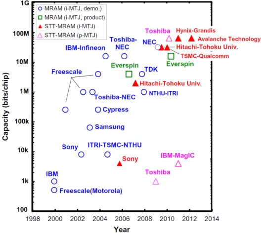
Figure 2.13 MRAM developments [36] ... 34
Figure 2.14 Racetrack memory based on CIDW motion ... 36
Figure 2.15 Cross-section structure of racetrack memory ... 36
Figure 2.16 Generic logic-in-memory architecture based on STT-MRAM. ... 38
Figure 2.17 Other spintronics based circuits ... 40
Figure 3.1 An example of PMA STT MTJ based on CoFeB/MgO stack ... 45
Figure 3.2 Diagram of the Landau-Lifshitz-Gilbert (LLG) equation. ... 47
Figure 3.3 Verification of the static model with measured data reproduced by [38] ... 49
Figure 3.4 Comparison of the dynamic model with measured data ... 52
Figure 3.5 Experimental measurements of STT stochastic switching behaviors [153]. ... 53
Figure 3.6 Diagram of integration of physical models into PMA STT MTJ ... 55
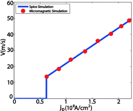
Figure 3.7 Dependence of DW velocity on current described by 1D model. ... 58
Figure 3.8 Good agreements with micromagnetic simulation for DW motion velocity as a function of current density. ... 59
xii
Figure 3.9 Dependence of cumulative probability of DW motion versus shifting current pulse
duration and magnitude. ... 60
Figure 3.10 Component Description Format (CDF) in Cadence ... 64
Figure 3.11 Symbol of the model PMA STT MTJ ... 65
Figure 3.12 (a) Symbol of the write head of racetrack memory; (b) Schematic of internal DW nucleation circuit integrated in the write head symbol. ... 66
Figure 3.13 Symbol of magnetic domain in magnetic nanowire. ... 66
Figure 3.14 Symbol of the read head of racetrack memory. ... 66
Figure 3.15 Schematic for the simulations of PMA STT MTJ. ... 68
Figure 3.16 DC simulation of PMA STT MTJ ... 69
Figure 3.17 Transient simulation of the PMA STT MTJ ... 70
Figure 3.18 100 complete writing operation simulations ... 71
Figure 3.19 Dependence of sensing bit error rate (BER_S) versus sensing current for different switching duration pulses. ... 71
Figure 3.20 Statistical Monte-Carlo simulation of the PMA STT MTJ with 1% variation of TMR ratio, oxide barrier and free layer thickness. ... 72
Figure 3.21 Simulation schematic of PMA racetrack memory. ... 73
Figure 3.22 Transient simulation of PMA racetrack memory driven by 50MHz I ... 74 p Figure 3.23 Transient simulation of PMA racetrack memory driven by 500MHz square wave Ip ... 75
Figure 3.24 Dependence of I current pulse frequency and energy dissipation versus CMOS die p area for one 8-bit racetrack memory. ... 76
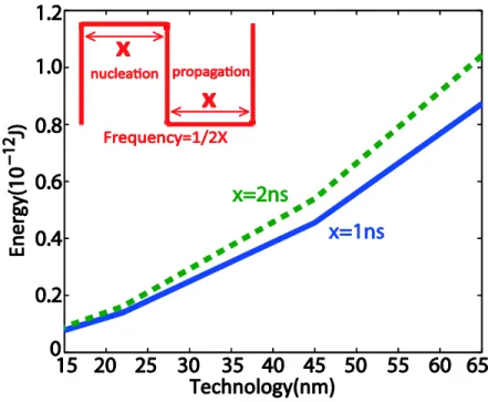
Figure 3.25 Dependence of energy dissipation and operating frequency versus racetrack memory technology node. ... 77
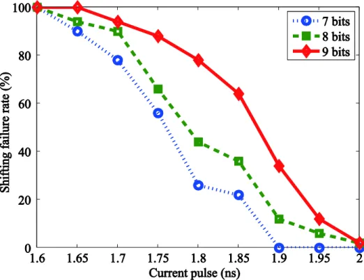
Figure 3.26 Dependence of shifting failure rate versus current pulse duration and racetrack memory capacity. ... 78
Figure 3.27 Layout of racetrack memory ... 79
Figure 4.1 Pre-charge sense amplifier (PCSA) ... 83
Figure 4.2 PCSA sensing operation ... 84
Figure 4.3 Dependence of chip failure rate on reading duration for different reading current. ... 85
Figure 4.4 Schematic for 16k-bits PCSA sensing circuit (m=16, n=1k). ... 86
Figure 4.5 Monte-Carlo simulation of a 16k-bit PCSA circuit. ... 87
Figure 4.6 Full writing schematic for STT writing approach ... 88
xiii
Figure 4.8 Dependence of circuit switching speed and energy dissipation versus die area ... 91
Figure 4.9 Monte-Carlo simulation of a whole writing operation implemented by the writing circuit. ... 92
Figure 4.10 Dependence of writing Bit Error Rate (BER_W) versus die area of writing circuit. . 93
Figure 4.11 1-bit STT-magnetic full adder (MFA) architecture ... 94
Figure 4.12 Transient simulations of 1-bit STT-MFA ... 97
Figure 4.13 One sensing operation of the PCSA based STT-MFA ... 98
Figure 4.14 Dependence of delay time and dynamic energy on the width of discharge transistor for STT-MFA. ... 99
Figure 4.15 Dependence of delay time and dynamic energy on the resistance-area product (RA) of PMA STT MTJ. ... 99
Figure 4.16 Dependence of delay time and dynamic energy on PMA STT MTJ TMR ratio for 1-bit STT-MFA. ... 100
Figure 4.17 CARRY circuit of multi-bit MFA based on PMA racetrack memory including MTJ writing circuit. ... 102
Figure 4.18 Transient simulation of proposed multi-bit MFA ... 103
Figure 4.19 Transient simulation of CARRY storage ... 104
Figure 4.20 Dependence of domain wall propagation delay on the transistor width of propagation circuit. ... 105
Figure 4.21 Dependence of energy consumption, switching speed and the energy-delay product versus the width of 4 transistors using in writing circuit. ... 106
Figure 4.22 Conventional content addressable memories (CAMs) [174-175] ... 109
Figure 4.23 (a) Structure of dual nanowires based RM-CAM. One writing current pulse nucleates a couple of MTJs with complementary configurations. (b) One example of current pulse configuration ... 110
Figure 4.24 Schematic of the comparison circuit ... 112
Figure 4.25 Schematic of an 8 x 8 bits RM-CAM ... 113
Figure 4.26 Transient simulations of the RM-CAM ... 114
Figure 4.27 Dependence of full area versus number of bits per word. ... 115
Figure 5.1 2-bit parallel multi-level cell (MLC) ... 122
Figure 5.2 2-bit serial MLC ... 123
Figure 5.3 Monte-Carlo simulations for 2-bit parallel MLC ... 124
Figure 5.4 Monte-Carlo simulations for 2-bit serial MLC ... 125
Figure 5.5 Tradeoff dependence of switching duration versus area and pulse magnitude for serial MLC. ... 126
xiv
Figure 5.7 Static simulations to evaluate voltage sources performances ... 130
Figure 5.8 Current source based on current mirror to optimize current amplitude and stability . 131 Figure 5.9 Dependence of nanowire length on shifting current for different current and voltage sources ... 132
Figure 5.10 Maximum nanowire lengths for magnetic DW motion LMax versus different magnetic material resistivity. ... 133
Figure 5.11 Short magnetic nanowire based racetrack memory ... 134
Figure 5.12 Direction of DW motion with the effects of current and field [182] ... 135
Figure 5.13 Structure of PMA Co/Ni racetrack memory with magnetic field assistance ... 136
Figure 5.14 Sectional view of the structure of PMA racetrack memory with magnetic field assistance ... 137
Figure 5.15 Generation of magnetic field by current ... 138
Figure 5.16 Relation between DW motion velocity and magnetic field ... 138
Figure 5.17 Transient simulation of 8-bit PMA racetrack memory with magnetic field assistance. ... 140
Figure 5.18 Transient simulation of 16-bit PMA racetrack memory with magnetic field assistance. ... 141
Figure 5.19 Dependence of maximal length of magnetic nanowire versus (a) critical current density of DW shifting at different nanowire thickness. (b) shifting NMOS (NM3) die area with different voltage supplies. ... 142
Figure 5.20 Dependence of magnetic field required and shifting energy versus different number of bits per nanowire in racetrack memory. ... 144
xv
List of Tables
Table 2.1 Comparison of various MRAM technologies ... 33 Table 3.1 Parameters in the compact models of PMA STT MTJ and PMA racetrack memory .... 63
Table 4.1 Truth table of “SUM” and “Co” logic gate for MFA ... 95 Table 4.2 Truth table and resistance configuration of “Co” for MFA ... 96
Table 4.3 Comparison of proposed 1-bit STT-MFA with CMOS only full adder ... 101 Table 4.4 Comparison of proposed 8-bit MFA based on racetrack memory with CMOS only full adder included transferring and writing data ... 108 Table 4.5 Comparison of CAMs based on different technologies ... 116 Table 5.1 Parameters in the compact models of PMA racetrack memory with magnetic field assistance ... 139
1
Chapter 1 Introduction
1.1 Motivation ... 2 1.2 Contributions ... 6 1.3 Organization of the thesis ... 8
2
1.1 Motivation
The manipulation of the charge of electron has dominated the electronic world for over six decades. Thanks to its solid physical foundation, incalculable charge-based electronic devices have been designed or truly applied for our life. One of the most well-known stories is about complementary metal-oxide-semiconductor (CMOS) technology, which plays a predominant role for integrated circuits nowadays. This relatively mature technology has been widely used in not only digital but also analog integrated circuits, for example, microprocessors, static random access memory (SRAM), image sensors and data converters. The evolution of CMOS technology
is commonly described by the famous Moore’s law that was observed by Gordon Moore in 1965.
It predicts that the number of transistors in integrated circuits doubles approximately every two years, which is, however, often quoted as 18 months afterwards. This prediction based on observation has continued for a long time, in turn, it has become a motive force to drive the researchers to innovate and develop the technologies.
Figure 1.1 ITRS power consumption roadmap. (Red line: Requirement of dynamic plus static power) However, with the shrinking of CMOS technology node below 90 nm, the growth of transistor number began to slow down. This is mainly due to the high static power dissipation in memory
3
and logic chip caused by the increasing leakage currents (see Figure 1.1). This power issue limits greatly the shrinking and improvement of electronic devices. For example, the design of multicore microprocessors for CPU in computer by many large semiconductor chips is a proof for this point.
In this background, novel technologies to replace the mainstream charge-based electronics are the hot topics for both academics and industries. Beyond the electrical charge, the spin freedom of electron attracts a broad attention and is considered to have a bright future. By being investigated for several decades, the spintronics was born from the discovery of Giant Magnetoresistance (GMR) effect and then rapidly developed. Figure 1.2 summarilizes the highlighted milestones for the development of the spintronics. The devices based on spintronics show the performance advantages in many aspects. The first one is low power. This is due to the non-volatility, which means that the information can be maintained without electrical power. With this feature, the system can be powered off in the idle state, which reduces greatly the standby power. Furthermore, spintronics can also allow reducing dynamic power that is normally caused by the large data traffic in the conventional Von-Neumann architecture. The possibility of spintronic devices to be 3D integrated above CMOS circuits at the back-end process can promise to significantly shorten the distance between memory and logic chip. Besides the power efficiency improvement, the potential advantages in terms of scalability and latency make the spintronic devices be used for various logic and memory applications. For example, spintronics has revolutionized ultra-high density Hard Disk Drives (HDDs) since the last 20 years.
4
Magnetic tunnel junction (MTJ), one of the most important spintronic devices, is the basic element of magnetoresistance random access memory (MRAM) which becomes a most promising candidate for the next generation of universal non-volatile memory. As a result of the tunnel magnetoresistance (TMR) effect, the MTJ resistance depends on the relative magnetization orientations of two ferromagnetic layers in MTJ. Much of the academic and industrial research efforts are presently focused on developing efficient strategies for switching magnetization in MTJs. One promising method relies on using spin transfer torque (STT), which involves low threshold currents and well-understood mechanisms. Furthermore, only a bi-directional current is needed in this approache, which simplifies greatly the CMOS switching circuits and thereby allows for higher density than the other approaches. However, some unexpected effects have been discovered using this approach in small MTJs (e.g. lateral size of 40 nm), such as erroneous state switching with reading currents and short retention times. These problems are mainly related to the in-plane magnetic anisotropy, which can not provide a sufficiently high energy barrier to ensure thermal stability. This issue limits greatly the potential for future miniaturization of MTJs. One compelling solution addressing this issue involves the perpendicular magnetic anisotropy (PMA) in certain materials (e.g. CoFeB/MgO), because it allows high energy barrier to be attained for small-size structure (< 40 nm) while maintaining the possibility of fast-speed operation, high TMR ratios and low threshold currents.
Racetrack memory is an emerging spintronic concept based on current-induced domain wall (CIDW) motion in magnetic nanowire. Combining with MTJs as write and read heads, CMOS integrability and fast data access speed can be achieved. In this concept, the data are stored via the magnetizations of magnetic domains separated by domain walls (DW). Due to STT mechanism, the DWs can be propagated consecutively in a direction by a spin current, which makes the racetrack memory possible to be widely applied for logic and memory designs. Considering the assets of PMA, the distance between the adjacent DWs can be extremely small, hence racetrack memory based on PMA materials is expected to provide ultra-high density. Thanks to the diverse advantages demonstrated by spintronics as wall as various milestone breakthroughs of its related materials and techniques, hybrid spintronics/CMOS logic and memory circuits open a novel route to manipulate information more efficiently. Taking advantages of spintronic devices, the emerging circuits or systems can also realize low power,
5
high density and high speed. For the past decade, many spintronics based logic and memory circuits and their prototypes have been designed and presented. From the relatively mature spin valve for HDDs to recently commercialized STT-MRAM, from magnetic full adder (MFA) for magnetic processors to magnetic content addressable memory (CAM) for internet router and search engines, spintronics or concepts based on it has seeped into a majority of the advanced logic and memory systems.
However, spintronics is still on the way. There inevitably exist a lot of obstacles to challenge its feasibility and application potential. For example, although STT-MRAM has recently been commercialized, its density cannot be comparable to that of mainstream memories (e.g. dynamic random access memory (DRAM)). This density issue has become the main bottleneck to hinder the further development of STT-MRAM, and many approaches have been proposed to overcome it. Among them, multi-level cell (MLC) is a feasible scheme. Similarly, the high threshold current for propagating DWs limits the density of racetrack memory. As a large capacity racetrack memory requires a long magnetic nanowire, the high resistance of magnetic nanowire makes it difficult to provide an enough high propagation current. The optimizations at the levels of circuit and material have been proposed, however, none of them can offer a not only feasible but also reliable performance. Indeed, CIDW motions can be triggered below the threshold current due to the Walk breakdown, which has recently been discovered. This interesting counterintuitive phenomenon may be an opportunity to achieve a practically large capacity racetrack memory.
6
1.2 Contributions
In view of the foregoing research background and motivation, this thesis is focused on the integration of spintronic devices. From compact modeling to circuit design and optimization, the contributions of this thesis have been made at a series of levels. The main research contributions of this thesis are as follows:
Compact modeling of PMA STT MTJ is firstly developed. By studying and
synthesizing the related physical models, STT static, dynamic and stochastic behaviors in PMA material structures are integrated. This compact model can contribute to test and explore the performance of individual cell or hybrid MTJ/CMOS circuits based on PMA STT MTJ.
Compact modeling of PMA racetrack memory is also developed. The physical model
describing CIDW motion in PMA magnetic nanowire is embedded. By combining with PMA STT MTJ compact models as write and read heads, the full system of PMA racetrack memory is carried out. This compact model can be used extensively in various emerging logic and memory circuits, which strongly stimulates the development and application of racetrack memory.
1-bit MFA based on PMA STT MTJ and multi-bit MFA based on PMA racetrack
memory are designed. Their performance advantages in terms of power, speed and density compared with the conventional designs indicate the prospectives for applying spintronic devices in computing logic applications.
A novel design of CAM based on PMA racetrack memory is proposed. Taking
advantage of 3D integration and sharing of CMOS writing and sensing circuits, this emerging design can achieve unprecedentedly high density and low power.
A PMA STT-MRAM based on MLC is designed to envisage the density issue. This
design utilizes innovatively the STT stochastic behavior, which is normally considered a negative side, to realize ultra-fast multi-level function. This design avails as well to improve the neuromorphic systems.
7
PMA racetrack memory with magnetic field assistance is proposed to overcome the
high threshold current issue. As mentioned above, this issue limits seriously the capacity potential of racetrack memory. Based on the recent observation involving DWs triggered by a low current under an external magnetic field, this design provides a new alternative for capacity improvement of racetrack memory and futher benefits for its feasibility and promotion.
8
1.3 Organization of the thesis
This thesis is organized into six chapters, including the introduction and the conclusion.
In Chapter 2, we introduce the state of the art concerning the work of this thesis, which includes the origine of the spintronics, the spintronic devices and the spintronic logic and memory circuits. The parts involving spintronic devices and circuits emphasize the MTJ and the racetrack memory that are the highlights of this thesis.
In Chapter 3, we present the compact modeling of PMA STT MTJ and PMA racetrack memory. The physical bases of them are elucidated in details, for example, STT static, dynamic and stochastic models for PMA STT MTJ as well as one-dimensional (1D) DW model for racetrack memory. The implementation of compact modeling in Verilog-A language is demonstrated. Diverse simulations (e.g. Direct Current (DC) simulation, transient simulation and statistical Monte-Carlo simulation) are carried out to validate the functionality of these compact models. In Chapter 4, we focus on the hybrid spintronics/CMOS circuit design with emphysis of PMA STT MTJ and PMA racetrack memory based logic and memory circuits. Two basic circuits, i.e. writing and sensing circuits, are firstly presented. Their operations and performances are involved. By using the compact models of PMA STT MTJ and PMA racetrack memory, MFA and CAM are respectively proposed and studied. In comparison with the conventional circuits, the performance of these spintronic applications in terms of power, speed and density are discussed. In Chapter 5, two design optimizations envisaged to overcome the density issues: MLC for STT-MRAM and magnetic-field assistance for racetrack memory, are successively proposed. From the structural implementation to the performance analyses, these optimized designs are thoroughly investigated and assessed.
In Chapter 6, the thesis will be globally concluded. Perspectives and future reseach directions will also be outlined.
The hierarchy of the work in this thesis can be depicted by Figure 1.3, which involves from the state variable to the architecture.
9
11
Chapter 2 State of the art
2.1 Spintronics ... 12 2.2 Spintronic devices ... 14
2.2.1 Magnetic tunnel junction (MTJ) ... 14 2.2.1.1 MTJ structure ... 14 2.2.1.2 Switching approaches for MTJ ... 16 2.2.1.2.1 Field-induced magnetic switching (FIMS) ... 16 2.2.1.2.2 Thermally assisted switching (TAS) ... 17 2.2.1.2.3 Spin transfer torque (STT) ... 18 2.2.1.2.4 Thermally assisted spin transfer torque (TAS+STT) ... 19 2.2.1.3 Perpendicular magnetic anisotropy (PMA) ... 19 2.2.1.4 Recent progress of MTJ ... 21 2.2.2 Magnetic domain wall (DW) nanowire ... 23 2.2.2.1 Current-induced DW (CIDW) motion ... 25 2.2.2.2 Recent progress of magnetic DW motion... 26 2.2.3 Other spintronic devices ... 28
2.3 Spintronics based hybrid logic and memory circuits ... 32
2.3.1 Magnetoresistance random access memory (MRAM) ... 32 2.3.2 Racetrack memory ... 35 2.3.3 Logic-in-memory ... 37 2.3.4 Other spintronic hybrid circuits ... 39
2.4 On-going big projects ... 41
2.4.1 MAGWIRE ... 41 2.4.2 MARS ... 41 2.4.3 Other projects ... 42
12
2.1
Spintronics
Spintronics (spin transport electronics or spin electronics) is an emerging interdiscipline whose principal idea is to control the electrons’ spin degrees of freedom for electronics. It is considered a potentially promising technology to replace the mainstream charge-based electronics [1]. The spin of the Electron has been known by public for almost 100 years. Although its theoretical and experimental studies were developed by many scientists and it was proven to play the key role in several areas of condensed matter physics, it was rarely involved with the conventional electronics based on charge of electrons [2]. The story had a twist in 1988 due to the Giant MagnetoResistance (GMR) effect that was respectively discovered by Albert Fert in France and Peter Grünberg in Germany [3-4]. GMR effect was observed in thin ferromagnetic structures, which is because: in paramagnets, the numbers of up-spin (majority) and down-spin (minority) electrons are the same, or it is to say that their spin direction is random; in ferromagnets, with the difference between the numbers of up-spin and down-spin electrons, the magnetism can influence the electrical transport, in turn the process can be reversed.
This outstanding research discovery is afterwards considered a milestone in physics, especially in condensed matter domain. Because of this, the Nobel Prize in Physics was awarded to both of these physicists in 2007. This discovery is also deemed as the “birth” of spintronics.
A fundamental understanding of spintronics can be explained by three main aspects: spin polarization, spin relaxation and magnetoresistance [5]. Firstly, in electrical spin injection, spin polarization is defined by the imbalance of spin population. As a current passing through a magnetic material can be polarized by the local magnetic moment, it will lead to the nonequilibrium spin accumulations [6]. Secondly, when the current carrying the spin-polarized electrons reaches and passes another magnetic material, spin relaxation will take place, which drives the spin population back to equilibrium. The length for situation wherein the spin keeps its direction is called the spin diffusion length [7]. A material parameter named damping constant is usually used to describe the speed of the spin relaxation. Thirdly, similar to the electrical resistance, there is a magnetoresistance for magnetic material. As it is found to be sensible to the nonequilibrium spin population, its changes are thus measured to detect the spin states.
13
Benefiting from this phenomenon, spintronic devices, not merely based on GMR effect, offer the possibility to integrate with hybrid process.
In details, GMR effect can be described by two channel model as shown in Figure 2.1. In the simplest form, two ferromagnetic (FM) layers are separated by a non-magnetic (NM) metal layer. When the magnetization directions of two FM layers are parallel, the spin-up electrons can pass through the structure nearly without scattering, providing a relatively low resistance. Contrarily, in the anti-parallel configuration, both spin-up and spin-down electrons will suffer from the scattering, which leads to a higher resistance. In some multilayers structure, the difference between the resistances in parallel and anti-parallel states can reach 100%, which is the reason why it is named by giant magnetoresistance. This outstanding effect soon attracts intense research attention. The concept “spin valve” is one of the most important applications based on GMR effect, which has been widely used in the hard disk drives (HDDs) as read heads [8]. At the
beginning, the “current in plane” (CIP) spin valve geometry was mainstream. The “current perpendicular to plane” (CPP) was afterwards found to be more convenient for the downscaling,
however more difficult to fabricate [9]. From 1997 to 2003, HDD’s area density has been increased by three orders of magnitude (from ~0.1 to 100 Gbit/in2) [10].
14
2.2 Spintronic devices
Beyond the spin valve mentioned above, there are a number of devices based on spintronics. Among them, magnetic tunnel junction (MTJ) and magnetic domain wall (DW) nanowire are no doubt the most promising ones thanks to their mature technologies and high performances. In this thesis, we will mainly focus on these two emerging spintronic devices and investigate their integrations in hybrid logic and memory circuits.
2.2.1 Magnetic tunnel junction (MTJ)
2.2.1.1 MTJ structure
Figure 2.2 MTJ structure
By replacing the non-magnetic metal layer by a thin insulating (e.g. AlxOy and MgO) layer, the magnetic tunnel junction (MTJ) is created as shown in Figure 2.2 [11-13]. In the inchoate types of MTJ, two FM layers have different coercivities (defined as the magnetic field to switch the magnetization). Then in the recent and mainstreams types of MTJs, one of the FM layers is pinned layer whose magnetization is fixed in a specific direction and the other is free layer whose magnetization can be tuned. Nowadays, it is considered as the basic element of magnetoresistance random access memory (MRAM) and provides a great impetus for electronics development.
With respect to the spin valve based on GMR effect, MTJ is related to Tunnel MagnetoResistance (TMR) effect. The spin-polarized electrons pass from one FM to the other by a tunnel effect with the conservation of spin direction (see Figure 2.3). Actually, this effect was observed and proposed by Jullière as early as 1975 [14]. By analyzing the phenomenon of
15
tunneling conductance, he summarized a physical model to describe the change of conductance between parallel (P) and anti-parallel (AP) magnetizations in two FM layers. The related tunneling magnetoresistance ratio can be defined as
AP AP P P P AP P G G G R R R R R TMR (2.1)
where RAP and RPare the resistances of anti-parallel and parallel states of MTJ, which have the inverse relationship with the conductances GAP and GP. The expressions of conductance and spin polarization are given by
2 1 2 1 M m m M P N N N N G (2.2) 2 1 2 1 m m M M AP N N N N G (2.3) ) ( ) ( mi Mi mi Mi i N N N N P (2.4)
where NMi and N are the effective densities of states of majority and minority electrons at the mi Fermi energy in both magnetic layers. As a result, the TMR ratio is expressed in terms of the spin polarization by 2 1 2 1 1 2 P P P P TMR (2.5)
Unfortunately, caused by the technical limitations, the experiment of Jullière was difficult to reproduce and the progress of TMR had been impeded for almost 20 years. The breakthrough occurred in 1994 by using amorphous Al2O3 as the tunneling barrier (insulating layer) to realize
the room temperature magnetic tunneling transport [12-13]. By optimizing the material and fabrication condition, the TMR ratio of this structure can reach up to 70%. Although this value is already much larger than GMR in spin valve, it is still far away from the requirement for spintronic applications, for example, high density MRAM requires at least 150% TMR at room temperature. Another considerable leap of MTJ is using a single-crystal MgO tunnel barrier that can provide even larger TMR, which is sometime called the giant TMR effect [15-16]. So far, the
16
TMR ratio record of MgO based MTJ can reach as high as 600% at room temperature [17]. These results are of great importance not only to avoid the CMOS process mismatch and parameter variation, but also to miniaturize the sense amplifier circuit area [18].
(a) (b)
Figure 2.3 Schematic illustration of electron tunneling in MTJ. (a) Magnetizations in two FM layers are parallel (P state). (b) Magnetizations in two FM layers are anti-parallel (AP state).
2.2.1.2 Switching approaches for MTJ
2.2.1.2.1 Field-induced magnetic switching (FIMS)
Field-induced magnetic switching (FIMS) is a field-only switching approach as shown in Figure 2.4 [19]. Due to its typicality and maturity, the first generation of MRAM was built based on this switching approach. In such mechanism, the magnetic fields are generated by two orthogonal current lines, for example, Iw works as the word line and Ib works as the bit line to switch the magnetization of free layer. This structure has an advantage in sensing, which is totally independent with the writing lines. However, the write selectivity based on the combination of two perpendicular pulses of magnetic fields, i.e. Hb and Hw, may result in narrow write margin and half-selectivity issues. Furthermore, the high currents (>10 mA) to generate magnetic fields
17
yield considerable power consumption meanwhile the electromigration effect limits its scalability. These issues hinder its commercialization. Thanks to the toggle switching patterned by Freescale, MRAM based on this advanced switching method was commercialized in 2006 [20]. However this approach cannot yet overcome the drawbacks of speed, density and power caused by using magnetic field for switching.
Figure 2.4 FIMS approach structure.
2.2.1.2.2 Thermally assisted switching (TAS)
Figure 2.5 TAS approach structure.
To improve the performances of write selectivity, power consumption and thermal stability, thermally assisted switching (TAS) was proposed (see Figure 2.5) [21-22]. It is worthy noting that an additional anti-ferromagnetic (AFM) layer is normally added above the free layer to pin
18
the free layer at the standby temperature. Its basic principle is that a current flowing through MTJ heats the magnetic layers above their magnetic ordering temperature to reduce greatly the required switching field [23]. Similar to the FIMS structure, two orthogonal current lines are installed to achieve write selectivity; in contrast, one (Ih) is used to heat the MTJ and the other (Ib) is used to generate the switching field. This approach promises relatively lower power, higher density and higher thermal stability comparing with the pioneering FIMS approach; however, the mandatory heating and cooling processes lower the operation speed, which makes TAS approach not competitive in the high speed logic applications.
2.2.1.2.3 Spin transfer torque (STT)
Figure 2.6 STT switching approach structure.
While the relative direction of magnetizations of two FM layers affects the flow of spin-polarized current in GMR and TMR structures, a reverse effect, called spin transfer torque (STT), was proposed independently by Berger and Slonczewski in 1996 [24-25]. They found that a spin-polarized current injected perpendicularly to the plane could equally influence the magnetizations. This interaction is attributed to angular momentum transferred from the polarized electrons to the local magnetization of the FM layer. Once the amount of electrons exceeding the threshold value (often represented by critical current or critical current density), the STT exerted by the current will switch the magnetization of the free layer of MTJ [26-27]. The STT switching approach was initially researched on GMR based spin valve [28-29], and then focused on the MTJ providing a significantly higher magnetoreisistance [30-31]. In MTJ, one FM layer acts as a polarizer for an electric current, which then transfers angular momentum by exerting a torque on the
19
magnetization of the other FM layer. This current-only approach simplifies greatly the switching process as it only requires a bi-directional current. Moreover, the magnitude of current for STT is normally less by an order than that for generating a large magnetic field. As a result, STT switching approach is widely considered the most promising one to be applied in the future MRAM applications, and we will concentrate to investigate the spintronic devices based on this switching approach in this thesis [32-33].
2.2.1.2.4 Thermally assisted spin transfer torque (TAS+STT)
Combining the aforementioned advantages of TAS approach and STT approach, thermally assisted spin transfer torque (TAS+STT) switching approach was proposed [34-35]. Like STT switching approach, only one polarized current flows through the MTJ to heat and switch simultaneously the free layer. When the temperature of MTJ is risen above the blocking temperature of the AFM layer associated to the free layer and the current exceeds the threshold value of STT, the magnetization of free layer will be switched. This combined approach can provide a good tradeoff among density, power and thermal stability, however, it still requires the supplementary time for cooling and power for heating, which is adverse to achieve high-speed low-power applications.
2.2.1.3 Perpendicular magnetic anisotropy (PMA)
To address the requirement of high-performance MTJ for the future logic and memory applications, there are usually five criteria to evaluate: small area, high TMR ratio, low STT switching current, capacity to withstand the standard semiconductor processing and high thermal stability. With the shrinking of size, the conventional MTJ with in-plane magnetic anisotropy becomes more and more difficult to satisfy these criteria. Recent material progress showed that the MTJ with perpendicular magnetic anisotropy (PMA) could offer lower switching critical current, higher switching speed and higher thermal stability compared with that with in-plane magnetic anisotropy [36]. These can be explained by the following theories.
The barrier energy and critical current of STT switching in the materials with in-plane magnetic anisotropy can be expressed as:
20 2 0 S C i H Vol M E (2.6) Vol H H H M g e I d ani ext S B i C ) 2 )( ( 0 0 (2.7) where HC is the coercive field, Hext is the external field, Hani is the in-plane uniaxial magnetic anisotropy field, Hd is the out-of-plane magnetic anisotropy induced by the demagnetization field,
0
is the permeability in the free space, M is the saturation magnetization, Vol is the volume of S the free layer,
B is the Bohr magneton, is the gyromagnetic ratio, e is the electron charge, m is the electron mass.On the other hand, the barrier energy and cirtical current in materilas with PMA are given as:
2 0 S K p H Vol M E (2.8) Vol H M g e I S K B p C0 (0 ) (2.9)
where HK is the perpendicular magnetic anisotropy field.
By comparing Eq. 2.6 and Eq. 2.8, as HK is higher than HC, PMA allows obtaining relatively high barrier energy with a small size. By comparing Eq. 2.7 and Eq. 2.9, as HK is much lower than Hd, the critical current for PMA materials can be significantly reduced.
From 2002, when the first MTJ with PMA was reported, this advantageous structure attracts a great deal of attentions from academics and industries [37]. A variety of material systems has been attempted, for example, rare-earth/transition metal alloys, multilayers and other alloy materials. However, they have not been able to truly realize low critical current and high thermal
stability at the same time. This situation didn’t change until the Ta/CoFeB/MgO structure was
revealed in 2010 [38-39]. Figure 2.7 demonstrates the excellent performances of this structure. It takes advantages of CoFeB-MgO interface anisotropy to provide a good tradeoff among the area (40 nm), critical current (~50 µA), thermal stability (40 kBT) and TMR ratio (>100%).
Thanks to the material and technical improvement of MTJ, especially MgO based MTJ with PMA, a lot of persistent and intensive efforts have been made for the past years to develop the
21
high performance MTJ based systems, such as MRAM [40-43] that will be introduced in the following sections.
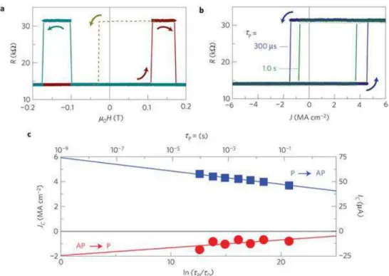
Figure 2.7 TMR and current-induced magnetization switching for Ta/CoFeB/MgO structure MTJ with PMA. (a) Perpendicular R-H curve. (b) Typical results of current-induced magnetization switching at current pulse duration of 300 µs and 1.0 s. (c) Critical current density as a function of pulse duration. [38]
2.2.1.4 Recent progress of MTJ
With the development of materials and techniques, there was a lot of progress for MTJ appearing during this thesis work. Here we mention briefly the most important and promising three of them, that are high spin torque efficiency in sub-volume regime, spin hall effect (SHE) and voltage-induced effect.
Along with the downscaling pace of MTJs beyond sub-volume limit (~40 nm), MTJ displays a relatively high thermal stability factor and low STT critical current. This so-called “high spin
torque efficiency” is a strong stimulus for high density MTJ application. Spin torque efficiency is
defined here as [188]: 0 c I E (2.10)
22
where E is barrier height (or thermal stability factor), and Ic0 is the average critical current. Spin torque efficiency reflects the capability of spin polarized current to reverse the barrier height. Practically, when the lateral size of MTJ sacling down to the sub-volume limite, sub-volume activation effects make the leading term guiding the magnetization switch in devices, which is negligible when lateral diameter is larger than the limit. Thanks to this effect, the scaling gain (faster operation, higher density and improved spin torque efficiency) can be further continued, which benefits greatly for the miniaturization of MTJ.
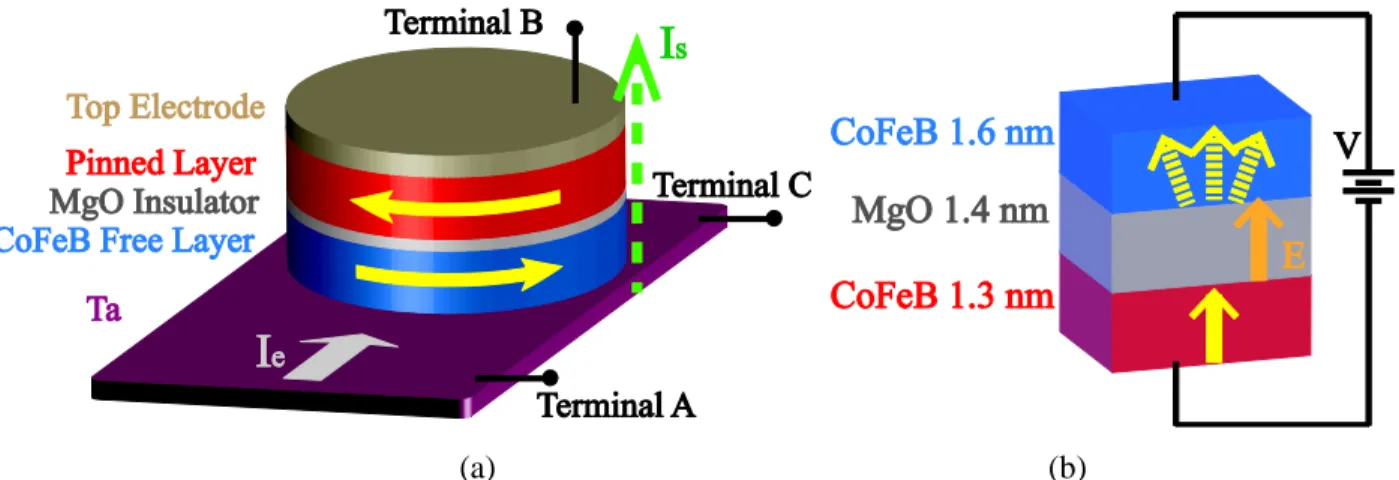
Beyond the STT switching mechanism, it has been discovered that a spin-polarized current can be generated by the SHE [44]. Due to the spin-orbit coupling, the electrons with different spins deflect in different directions. However, this effect was usually too modest to limit its application. Recently, it was reported that a giant SHE in a high-resistivity from of tantalum (β-Ta) could generate a spin current strong enough to induce the switching of MTJ [45]. Based on this prominent phenomenon, a three-terminal SHE device was proposed as shown in Figure 2.8(a). The electric current flowing horizontally induces a spin current to pass vertically through the in-plane MTJ structure. As the spin polarization of spin current is governed by the direction of the electric current, the magnetization switching direction of MTJ depends thus on the sign of electric current.
Although this three-terminal device would cause area efficiency degradation compared with the conventional MTJ, it exhibits various assets in many aspects. For example, by optimizing the thickness of Ta layer, the switching current can be decreased by nearly one order of magnitude compared with STT switching mechanism. The reduction of switching current and lower resistance of Ta layer can also lead to an advantageous switching energy. In addition, two-terminal MTJ always suffers from the reliability issue due to different resistance requirements for writing and sensing operations: low resistance is expected for writing operation and high resistance is more suitable for sensing operation. Three-terminal device separates the writing and sensing operations structurally, solving properly the reliability challenges. Thanks to these assets, this SHE based MTJ structure is regarded to have great potential towards the future magnetic memory and non-volatile logic design.
From the aforementioned introduction, we can find that the magnetization switching of MTJ has generally been carried out by either magnetic field or spin-polarized current. As the generation of
23
magnetic field is also implemented by the electric current, we can say that both of the above switching mechanisms are based on current, and then consuming energy. Beyond the spin-polarized current, voltage-induced effects provide another possible alternative to manipulate the magnetization [46-47]. It was recently observed that the interfacial perpendicular anisotropy can be controlled by the applied bias voltage. This is due to spin-orbit coupling which makes the surface anisotropy be modulated by the accumulated charge near the interface. From the point of view of implementation, there are two voltage-based switching mechanisms that have recently been exhibited. The first one is applying an ultra-fast voltage pulse to result in temporal change of magnetic anisotropy [48]. A toggle magnetization switching process under a constant bias field is realized by controlling the pulse duration of voltage. In the second one, the coercivity of ferromagnetic layers can be modified by the voltage-controlled interfacial anisotropy [49]. Based on this phenomenon, electric-field-assisted switching in MTJ has been successfully achieved (see Figure 2.8(b)). These voltage-controlled or electric-field-induced implementations require no current or just a very small current to switch MTJ, which offers a new path towards ultra-low power MRAM and logic systems.
(a) (b)
Figure 2.8 (a) Three-terminal device based on the giant spin Hall effect in β-Ta/CoFeB. (b) Electric-field-controlled switching in a CoFeB/MgO/CoFeB MTJ with interfacial PMA.
2.2.2 Magnetic domain wall (DW) nanowire
Magnetic domain walls (DWs) are the transition regions separating the domains with distinct magnetization direction, in which the magnetization vectors indeed rotate continuously [50]. From the 1960s, as DWs were considered to have a great potential application for future logic
24
and memory devices, intensive studies have been carries out to deepen both experimental and theoretical understandings [51]. At first, “magnetic bubble” materials were particularly investigated to realize magnetic bubble memories, wherein the magnetic bubbles or domains can be created and propagated in only one direction under an external magnetic field in thin films [52]. Each of bubbles stands for one bit of data and they are separated by the boundaries of bubbles, which can be considered as a kind of DW. As the magnetic bubble is very small and can be propagated along a series of parallel tracks, bubble memory was considered as a promising
technology to achieve “universal memory” that could provide high density and performance to
meet all storage needs. Although most of the bubble material based devices failed to be commercialized, the substantial theories and experimental developments effectuated at that time, in particular, the basis of DW dynamics based on Landau-Lifshitz-Gilbert (LLG) equations, were playing a vital role up to now [53].
As for the withdrawing of magnetic bubble memory from the history, there are principally two reasons: one is the introduction of other more competitive technologies, for example, hard drive and other semiconductor memory; the other one is the limitations of itself. Since most of bubble-based devices uses magnetic field to control magnetic bubble motion, large space cost is required for the generation of magnetic field. In addition, the speed of magnetic bubble motion is relatively limited for the extensive application. Nevertheless magnetic bubble memory is the first concept applying the field-induced DWs to store information.
With the development of nanolithography techniques, well-defined shape rather than large film can be patterned. One of the most successful applications of field-induced DW motion in sub-micrometer magnetic nanowire was to realize magnetic logic [54]. These logic gates consumed ultra-low dynamic power if we didn’t take into account the magnetic field generation, which operated as the clock of logic circuits. The logic state was non-volatile allowing zero standby power to keep the computing results. However these circuits also had critical shortcomings for practical applications due to magnetic field. For instance, their speed was low (e.g. <100 kHz) and the magnetic field generation with advanced CMOS circuits was a big challenge to manage the power dissipation. In this case, with respect to the limitation of magnetic field-induced DW motion, current-induced DW (CIDW) motion is more recently reported and will be introduced below.
25
2.2.2.1 Current-induced DW (CIDW) motion
The concept of current-induced DW (CIDW) motion was firstly proposed by Berger in 1978 [55]. The spin direction of electron is changed from the magnetization direction of one domain to that of the other domain when the electron crosses a DW. This change can be regarded as an angular momentum change. A reaction torque is induced on the DW to conserve angular momentum. And this torque transferred from the electrons leads to a direction change of the local magnetization moment, which results in DW motion. From 1984, Berger and his collaborators presented continuously a series of theories and experiments concerning the exchange interaction between electrons and DWs [56-59]. They demonstrated that the DW velocity could reach dozens of m/s by applying a current with current density in the order of 1010 A/m2 and microsecond long pulse. However, due to the limited fabrication techniques, this early work was mainly based on wide and thick NiFe films. Some additional current-induced effects (e.g. Eddy current and self-field effect) might be introduced to drive DW motion, which made the analyses of CIDW motion be much more difficult.
In 1996, STT effect was first predicted theoretically by Slonczewski and Berger [24-25], in which a spin polarized current can exert torque on magnetic moment and reverse the magnetization direction. It is extensively used in manipulating magnetization and controlling DW dynamics. This effect was later confirmed experimentally and drew enhanced attentions on magnetic devices based on CIDW motion.
Thanks to the advances in nano-fabrication and measurement techniques, the nanowires with the size below 100 nm can be patterned [60-62]. This form has a lot of advantages. Firstly, it minimizes greatly the self-field effect generated by the current flowing through the system, which allows us to investigate CIDW motion more ideally. Secondly, the width of nanowire can be smaller than that of DWs, which allows a single DW created to across the nanowire.
Lots of materials have been used to fabricate the nanowires, for example, single layer permalloy [56] and ferromagnetic semiconductor GaMnAs [63], etc. In our work, we mainly study the CIDW motion in magnetic nanowire with PMA, which has been revealed to require much less current density for DW propagation than those with in-plane magnetic anisotropy [64]. So far, there are actually certain PMA materials demonstrating a steady and pure CIDW motion, for
26
example, (Pt/Co)m [65-66], Pt/Co/AlOx [67] (see Figure 2.9), Co/Ni [68-70] and CoFeB/MgO
[71-73]. Among them, by exhibiting entirely interfacial PMA and large TMR ratio, CoFeB/MgO structure is promising to implement CIDW motion based devices.
Figure 2.9 (a) Kerr microscope image of the Pt/Co/AlOx nanowire with schematically shown Au constacts. (b) Differential Kerr microscope image of CIDW motion in Pt/Co/AlOx nanowire. [67]
2.2.2.2 Recent progress of magnetic DW motion
Recently, various emerging phenomena of CIDW have been demonstrated. Among them, electric-field-controlled effect and spin-orbit torque (SOT) draw undoubtedly the widest attention. Similar to the electric-field-controlled switching in MTJ, electric-field control of DW motion has also been observed in ultra-thin film with strong PMA, such as Pt/Co/AlOx [74-75] and
Pt/Co/GdOx (see Figure 2.10(a))[76-79]. The control behavior is displayed by tuning the DW
velocity via modulation of magnetic anisotropy. As it is a mechanism using gate voltage instead of current, ultra-low power can be expected. By enhancing or alleviating the DW velocity, pinning or depinning of DW can be operated. However, the experimental observations show that electric-field-controlled effect only impacts DW in its thermally activated creep regime and is still too weak for the case of high-speed DW motion, e.g. CIDW motion. The key challenge of this technology is to find a system with enhanced voltage-controlled magnetic anisotropy effect as well as large magnetoresistance. It is more recently reported that, in a specifically patterned structure, the pinning strength can reach as high as 650 Oe, enough to halt DWs with a speed of
![Figure 3.5 Experimental measurements of STT stochastic switching behaviors, high writing current drives faster speed and higher switching probability [153]](https://thumb-eu.123doks.com/thumbv2/123doknet/14529195.723306/72.918.261.670.346.673/figure-experimental-measurements-stochastic-switching-behaviors-switching-probability.webp)


![[PDF] Cours langage C++ : classes, Héritage et Polymorphisme | Formation informatique](data:image/gif;base64,R0lGODlhAQABAIAAAP///wAAACH5BAEAAAAALAAAAAABAAEAAAICRAEAOw==)