K. Brinkman,a)Y. Wang, M. Cantoni,b)D. Su,c)and N. Setter Ecole Polytechnique Fédérale de Lausanne (EPFL), Ceramics Laboratory, CH-1015 Lausanne, Switzerland
P.K. Petrov
Centre for Physical Electronics and Materials, London South Bank University, London SE1 0AA, United Kingdom
(Received 17 July 2006; accepted 12 October 2006)
Thin films of Pb(Sc1/2Ta1/2)O3(PST) were fabricated using an optimized chemical
solution deposition procedure involving the de-hydration of scandium acetate and the addition of up to 30% excess lead in solution. The choice of substrate was found to impact the thermal induced stress in the films as confirmed by wafer bending and in-plane grazing angle x-ray diffraction measurements. The presence of either a compressive or a tensile in-plane stress led to a reduction in the temperature of the dielectric maximum, whereas the value of the dielectric maximum remained relatively unchanged; its value reduced by an order of magnitude compared with ceramic samples. It is concluded that mechanical stress alone is not the sole factor in the reduction of PST thin film permittivity. Microstructural features resulting from
processing induced defects or an incomplete transformation to the relaxor state may be responsible for this commonly observed phenomenon.
I. INTRODUCTION
Thin film ferroelectric relaxors are of intense interest due to the remarkable dielectric and piezoelectric prop-erties exhibited in their single crystal counterparts.1
However, consistent experimental investigations by the ferroelectric community have confirmed the low-dielectric constant of relaxor thin films in a wide variety of materials such as lead magnesium niobate (PMN),2,3
lead magnesium niobate-lead titanate (PMN-PT),4 lead scandium niobate (PSN),5,6and lead scandium tantalate (PST).7–9Thin film relaxor PST10 and PMN11were re-cently shown to possess similar lattice dynamics com-pared with their bulk counterparts. The appearance of polar nanoregions as observed by Fourier transform in-frared (FTIR) studies confirmed that the defining feature of relaxor structure, namely the existence of polar nano-regions is qualitatively similar in bulk and thin films. Exactly why the permittivity is low in thin film relax-ors remains the subject of current controversy; however,
it is possible that this reduction of permittivity is due to processing-induced factors in thin film fabrication. In conventional ferroelectric materials such as lead zirconium titanate, it is well known that defects such as oxygen and lead vacancies may impact the polarization fatigue response in films fabricated from a variety of processing methods including pulsed laser deposition (PLD), chemical vapor deposition (CVD), sputtering and chemical solution deposition, or sol-gel.12–14 Polycrys-talline materials, such as those fabricated using a chemi-cal solution deposition technique have large grain bound-ary areas that also serve to increase defect concentra-tions. It has been proposed that defects may impact polarization reversal and act as pinning centers,15,16and recently there has been direct observation of this phe-nomenon.17
In addition, in chemical solution derived films, the pathway from an amorphous to a final crystalline state passes through an intermediate phase whose structure and stoichiometry is often different than the desired final phase.18–20 Theoretical work has recently revealed that inhomogeneities and concentration gradients may act as an effective internal field that smears out the phase tran-sition21and reduces the permittivity. The low tempera-tures used in thin film annealing coupled with point de-fect formation may significantly afde-fect the local structure and properties of the final crystalline phase.
Recent experimental findings for relaxor thin films comparing the “in-plane” and “out-of-plane” dielectric a)
Address all correspondence to this author.
Present address: AIST, Tsukuba Central 5, Tsukuba 305-8565 Japan.
e-mail: [email protected] b)
Present address: SB-CIME, Ecole Polytechnique Fédérale de Lausanne (EPFL), Lausanne, Switzerland.
c)
Present address: Dept. Materials Science and Engineering, University of Illinois-Urbana Champaign, Urbana, IL.
response in PST showed that the small film permittivity is truly a property of the film, and not the result of a surface passive layer.22 A renewed drive for thin film fabrication and characterization is therefore necessary if these materials are to meet their high expectations in actuator and capacitor applications. The subject of the current article is therefore an examination of the proc-essing and properties of the well-known ferroelectric re-laxor lead scandium tantalate by a chemical solution deposition method.
It is well known that the dielectric response of lead scandium tantalate (PST) is sensitive to “B” site order as controlled by annealing conditions. It has been demon-strated in ceramics23 and single crystals24 that ordered PST behaves as a conventional ferroelectric, whereas dis-ordered PST exhibits relaxor ferroelectric behavior. Re-laxor behavior in PST thin films was typically observed after low processing temperatures near 700 °C,7–9,25 whereas ceramic sintering conditions for disordered PST were significantly higher near 1500 °C.26,27 In the ma-jority of studies of PST for infrared detectors operating in the bolometer mode, a significant degree of ordering is sought because this increases the sharpness of the phase transition and enhances the DC bias induced pyroelectric properties. The current article focuses on disordered thin films processed at a temperature of 700 °C.
Lead scandium tantalate was initially fabricated in the thin film form by physical-vapor-deposition methods that followed procedures similar to traditional ceramic proc-essing. ScTaO4and PbO were sputter deposited in
alter-nating layers and subsequently reacted by high tempera-ture annealing above 900 °C to promote diffusion and obtain the desired perovskite phase.28
PST has been suc-cessfully prepared by sputtering,29
pulsed laser deposi-tion,30and CVD,8in addition to chemical solution depo-sition methods. The most recent work focuses on films sputtered at low temperatures near 300 °C, followed by post annealing at intermediate temperatures near 500 °C.31 Chemical solution processing of PST essen-tially began in the early 1990s with work by Whatmore et al. employing the two step method of depositing a ScTaO4layer followed by PbO deposition and reaction at
elevated temperatures.20,32 Liu and Payne33 prepared PST from a mixed acetate and alkoxide route using MOE as a solvent and Fuflyigin34 later fabricated PST from nitrate-based precursors in MOE solvents.
A variety of substrates have been utilized for PST film growth affecting the microstructure, crystallinity, and film properties. Specifically, the choice of substrate af-fects the mechanical boundary conditions of the thin films. Lattice mismatch induced strain is of importance for thin epitaxial films. In addition, differences in ther-mal expansion between the film and substrate induce residual stress. Pertsev has analyzed the effects of mechani-cal boundary conditions in conventional ferroelectrics
PbTiO3 and BaTiO3 35
using phenomenological argu-ments, however the situation is somewhat different in relaxor thin films. Firstly, due to their macroscopically cubic structure and the absence of any real structural phase transition, the effects of stress on orientation of a certain polar axis may not apply. Secondly, the dielectric maximum in relaxors is a dynamic phenomena resulting from the relaxation of polar nano regions embedded in a non-polar matrix and cannot be described by equilibrium Landau Ginzberg Devonshire formulations. Thirdly, there are still discrepancies in the literature as to the shift in the temperature of the dielectric maximum (Tm).
For example, epitaxial PMN-PT thin films PLD de-posited on LAO and MgO substrates showed compres-sive (positive in plane strain) and tensile (negative in-plane) strain, respectively.36 The temperature of the di-electric maximum (Tm) shifted to higher temperature and
the value of the permittivity maximum decreased under compressive strain; while the Tm shifted to lower
tem-peratures and the permittivity increased under tensile strain. However, later studies on PMN films deposited on MgO revealed the completely opposite effect; namely, compressive in-plane strain shifted the temperature of the dielectric maximum (Tm) to lower temperatures.
37
In ad-dition, it is known in bulk materials that the transition temperature may be shifted down with processing-induced defects such as lead vacancies so that the effects of stress and strain on the dielectric properties of relaxor thin films are far from being completely understood. This report examines processing issues in chemical solution derived PST thin films including the impact of the sub-strate on the position and value of the dielectric maxi-mum.
II. EXPERIMENTAL
Lead scandium tantalate films were prepared using chemical solution deposition techniques with solutions and precursor preparation performed in an inert Ar atmosphere using Schlenk Line techniques. In this study, the B site complex was synthesized from: (i) Sc acetate hydrate (Aldrich) and Ta ethoxide (Aldrich) (mixed al-koxide/acetate precursors) in a procedure similar to that described by Liu33; as well as from a new route (ii) pure alkoxide B site precursors Sc isopropoxide and Ta ethox-ide (Aldrich). All chemicals used in this study were pur-chased from Aldrich, St. Louis, MO. Details of the B site solution synthesis procedures are discussed in the fol-lowing section (Sec. III). Lead acetate tri-hydrate was used as the lead source and the solvent was 2-methoxy-ethanol (MOE). The lead precursor was first dissolved in MOE followed by reflux and vacuum distillation to re-move the excess water. The dehydrated lead acetate was then re-dissolved in MOE and mixed with the Sc/Ta complex to obtain the final PST solution.
Excess lead was added to the solutions in the amount of 10%, 20%, and 30% and films were fabricated both from pure solutions containing a given amount of lead, as well as from internal layers containing 10% lead, with top layers of 30% lead to compensate for the enhanced surface lead loss.38
Films were deposited by spin coating at 3000 rpm for 30 s followed by pyrolysis at 400 °C for 1 min; multiple layers were deposited before the film was rapid thermal annealed (RTA Process Products Corp., Andover, MA, RTM 2016) at 700 °C in flowing oxygen for durations between 1 and 20 min; 100 nm thick Pt bottom electrodes with Ti adhesion layers were deposited on silicon oxide passivated Si substrates by sputtering in a Nordico sputtering system (Fremont, CA).
Thermal gravimetric analysis (TGA) was carried out on a Mettler TA50 Thermal Analysis System (Columbus, OH) with powders heated at a rate of 10 °C per min to the final temperature in an air atmosphere. The typical sample weight was on the order of 10 mg. Fourier transform infrared (FTIR) spectra were obtained using a Nicolet 510 spectrometer (Madison, WI) equipped with an attenuated total reflection (ATR) crystal. Scanning electron microscopy (SEM) was performed on a Philips XL30 (Eindhoven, The Netherlands) equipped with an energy dispersive x-ray analysis detector (EDX). Trans-mission electron microscopy (TEM) was performed on a Philips EM430 ST with built-in EDX detector. X-ray diffraction was performed on a Siemens Kristalloflex 805 (Munich, Germany) with Cu K␣ radiation. The di-rect measurement of thin film stress was analyzed by measuring the radius of curvature of the substrate using a laser reflection technique (Tencor FLX-2900, San Jose, CA). The in-plane lattice strain was deter-mined from grazing angle x-ray diffraction measure-ments.39
Dielectric measurements of the films were made in this study in the “in-plane” and “out-of-plane” measure-ment configuration. In the “out-of-plane” measuremeasure-ment geometry Pt top electrodes were sputter deposited at room temperature and post-annealed at 650 °C 1 min. In the “in-plane” measurement configuration, Cu/Cr elec-trodes were sputter deposited on the film surface using photolithographic techniques to precisely define the electrode geometry and gap width. The film capaci-tance and loss tangent were measured using a Hewlett Packard HP 4284A LCR meter (Palo Alto, CA) con-nected to a temperature chamber with controlled heating and cooling rates of 2 °C /min from 100 to −100 °C. The dielectric response “in plane” was calculated using the partial capacitance of the film, substrate, and air compo-nents as described by Vendik in Ref. 40. Previously re-ported results in the PST thin films system includ-ing geometrical details as well as calculation of the di-electric constant from the gap capacitance are given in Ref. 22.
III. SOLUTION SYNTHESIS AND EFFECT OF “B” SITE COMPLEX
It has been demonstrated in the ABO3perovskite
sys-tems that the final crystal structure is impacted by the nature of the B site complex in solution.41,42
In chemical solution processed PST, it has even been observed that the order of mixing impacts the solution structure and final film crystallinity. A and B site mixtures of Pb and Sc prepared before the later addition of Ta led to higher levels of pyrochlore secondary phase than B site mix-tures of Sc/Ta followed by Pb addition.33,43In this work, B site precursors were prepared by combining Sc iso-propoxide and Sc acetate precursors with Ta ethoxide. A. Sc acetate dehydration procedures
In the case of the B site complex comprised of Sc acetate and Ta ethoxide, stoichiometric control, as well
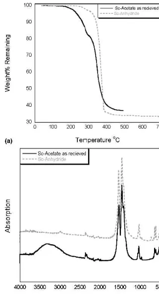
FIG. 1. (a) TGA of Sc-acetate as received and Sc-acetate purified in acetic acid anhydride. (b) FTIR spectra from Sc-acetate as received and Sc-acetate purified acetic acid anhydride.
as the tantalum precursor’s sensitivity to water necessi-tated a procedure to remove the hydrate from the starting precursor. This is demonstrated in Fig. 1, which shows the (a) TGA and (b) FTIR of the as-received scandium acetate indicating two major decomposition steps; the first from approximately 150 °C to 300 °C, and the sec-ond between 300 and 400 °C. The overall measured weight loss upon heating scandium acetate to scandium oxide was 63%, or 37% weight remaining compared with the theoretically calculated value of 31% weight remain-ing. The 6% weight difference between the measured and calculated value is attributed to bound and absorbed water in the starting precursor as confirmed by FTIR studies.
The FTIR of the scandium acetate powder displays a broad vibration band at 3500 cm−1 attributed to water, the symmetric and asymmetric acetate stretch bands cen-tered at 1500 cm−1, C-O-M stretches observed in the 1000 cm−1region, and a generally broad and noisy M-O region around 500 cm−1. Because the first decomposi-tion step has a weight loss of 15%, and extends to near 300 °C; it is likely that this is a combination of weight loss from water groups up until approximately 220 °C (weight loss approximately 6%), followed by the start of the acetate decomposition from weakly bound ace-tate groups. The second decomposition step from 300 °C to 400 °C corresponds to acetate decomposition, which finished at approximately 450 °C: Two methods were investigated for the dehydration of scandium acetate: (i) a reaction of scandium acetate hydrate with acetic anhydride with the resulting precursor termed Sc-anhydride and (ii) a reaction of scandium acetate hydrate with MOE with the resulting precursor termed Sc-MOE.
1. Sc-anhydride
In the case of the Sc-anhydride dehydration method, the water is removed by reaction with acetic anhydride to form acetic acid. Figure 1 shows the TGA and IR of scandium acetate after refluxing in acetic anhydride sol-vent at 130 °C for 2 h before vacuum distillation and vacuum drying at 60 °C for 1 day. The TGA indicates one-step decomposition, suggesting the decomposition of a single chemical species with a measured weight loss of 68% or remaining weight of 32% compared with the calculated 31% theoretical remaining weight. The IR shows the absence of water vibrations at 3500 cm−1and a slightly modified acetate stretch region including a sharper, less broad acetate absorption peaks than Sc-MOE and a change in the relative intensities of the sym-metric and asymsym-metric acetate stretch peaks compared to Sc-MOE and Sc-acetate. The scandium anhydride method is successful in precursor dehydration and results in a homogenous starting precursor.
2. Sc-MOE
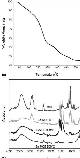
In the case of Sc-MOE, the water is removed upon distilling the minimum boiling point azeotrope, which forms between water and the solvent. In Fig. 2(a) the thermogravimetric analysis shows the behavior of Sc ac-etate after being refluxed 12 h in MOE under inert argon, vacuum distilling and vacuum drying for 12 h. We see a different decomposition behavior from the as-received scandium acetate, with four major decomposition steps present in the precursor: (i) from room temperature to approximately 240 °C, (ii) 240 °C until approximately 320 °C, (iii) 320 until 400 °C, and (iv) 400 to approxi-mately 550 °C.
The overall measured weight loss is 65% or 35% of the weight remaining after transformation into scandium oxide, compared with the 31% remaining weight
FIG. 2. (a) TGA of Sc-MOE, scandium acetate precursor after ex-tended reflux in MOE solvent. (b) FTIR of Sc-MOE as a function of temperature.
theoretically calculated for decomposition of scandium acetate. The initial weight loss up to 200 °C is attributed to the removal of MOE solvent present even after the vacuum drying step as well as bound and absorbed water; both are evidenced by the room temperature IR spectra of Sc-MOE powder shown in Fig. 2.
The corresponding spectra of pure 2-MOE is indicated for comparison showing OH vibrations in the 3500 cm−1
range, alkoxy and aliphatic resonances from MOE in the 3000 cm−1region, and C-O-M stretches (MOE) around 1000 cm−1. The IR spectra of the Sc-MOE powder shared the same MOE vibrations at 3000 and 1000 cm−1, as well as the acetate stretch region at 1500 cm−1. The IR spectra of the same powder after vacuum drying and subsequent heating to 300 °C and 500 °C showed the presence of MOE vibrations in the spectra at elevated temperature above the boiling point of MOE. The final decomposition from 400 °C to above 500 °C may be at-tributed to a more stable species bound to the scandium than the acetate group whose previous decomposition was seen to be complete at 400 °C.
The presence of MOE vibrations at elevated tempera-tures as seen by IR and the multiple step decomposition as compared to non-MOE modified scandium acetate suggests that the structure of the starting compound was modified by refluxing at 120 °C for 12 h in the MOE solvent resulting in a ligand exchange reaction between the Sc acetate and MOE. This method is deemed capable of dehydrating the starting compound; however, the re-sulting changes in the precursor structure make the mo-lecular weight determination and resulting film stoichi-ometry difficult to control.
B. “B” site complex
1. Sc isopropoxide and Ta ethoxide
Scandium isopropoxide (Aldrich) was combined with Ta ethoxide (Aldrich) in the MOE solvent and held at a reflux temperature of 120 °C for 5 h. The resulting double alkoxide complex exhibited excellent stability and could be stored for long periods in containers sealed in an Ar ambient without signs of precipitation or color change. The Sc/Ta double alkoxide was then further combined with lead dehydrated in MOE as described in the following section and held at a reflux temperature of 120 °C for 3 h in MOE before being vacuum distilled to a concentration of 0.5M. PST solutions derived from Sc isopropoxide with 20% added excess lead were deposited onto Pt/Si substrates and structural and dielectric char-acterization was performed. Figure 3 displays the x-ray diffraction spectra showing a (111) oriented phase pure perovskite crystal structure. However, the microstructure was porous in nature with surface defects resulting in the poor dielectric properties displayed in Fig. 3(c). This was in contrast to the well developed, dense grain structure in
FIG. 3. (a) X-ray of 600 nm PST containing 20% excess lead from Sc isopropoxide precursor; (b) SEM; and (c) dielectric constant and loss tangent at 1 kV/cm AC field.
Sc acetate derived films. Due to their superior micro-structural development, the remaining sections of this article discuss films fabricated from Sc-acetate derived precursors.
2. Sc acetate and Ta ethoxide
Sc-anhydride and Sc-MOE precursors were subse-quently reacted with tantalum ethoxide (vacuum dis-tilled), forming a Sc/Ta complex that was combined with lead acetate (10% excess in this case) to obtain the final PST sol. Experiments showed that the use of the Sc-anhydride directly with the tantalum precursor resulted in a quick reaction forming a clear and colorless Sc/Ta com-plex (after 4 h at 130 °C); however, this formed an un-stable PST solution that quickly precipitated within a few days. Before precipitation, sol-gel solutions were al-lowed to dry at 100 °C in air to promote gel formation and were subsequently calcined in a box furnace at 1000 °C for 2 h in air using a sealed crucible. PST pow-ders made from Sc-anhydride precursor solutions led to high quantities of a pyrochlore secondary phase.
In the case of PST prepared using a Sc-MOE precur-sor, the reaction to form a clear and colorless Sc/Ta com-plex took over 12 h when refluxed at 120 °C, and the resulting solution was stable upon cooling when stored in an Ar atmosphere for months after synthesis. The struc-tural modification of the Sc precursor by the MOE sol-vent was thus seen to impact the reactivity and stability of the Sc/Ta complex (longer reaction times and more stable Sc/Ta complex as compared to Sc-anhydride), which led to increased perovskite phase formation.
Although this is empirical evidence, and detailed chemical and structural studies have not been performed on the system, the link between perovskite phase forma-tion and “B” site precursor homogeneity has been previ-ously established in other material systems.44Pyrochlore phases in the PST system are usually Ta rich and Sc deficient.32 Because lead content and processing condi-tions were the same in the Sc-MOE and Sc-anhydride derived PST solutions, the pyrochlore phase observed in our case is likely linked with the “B” site species. There-fore we can hypothesize that it was an in-homogenous Sc/Ta complex that led to a high degree of pyrochlore phase for Sc-anhydride, in agreement with studies of mixing order effects in PST chemical derived solu-tions.33,43
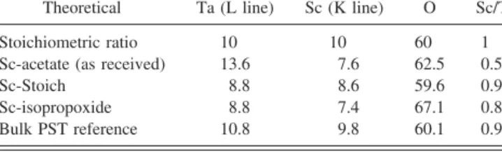
The success of the Sc dehydration procedure and proper solution mixing is ultimately seen in the stoichi-ometry of the resulting films. The composition of films made from solutions with different scandium precursors is presented in Table I. Table I displays stoichiometric deviations of Sc/Ta ratio of 0.56 obtained from using as-received scandium acetate without the dehydration step, compared to 0.98 Sc/Ta ratio obtained by using a dehydrated scandium precursor.
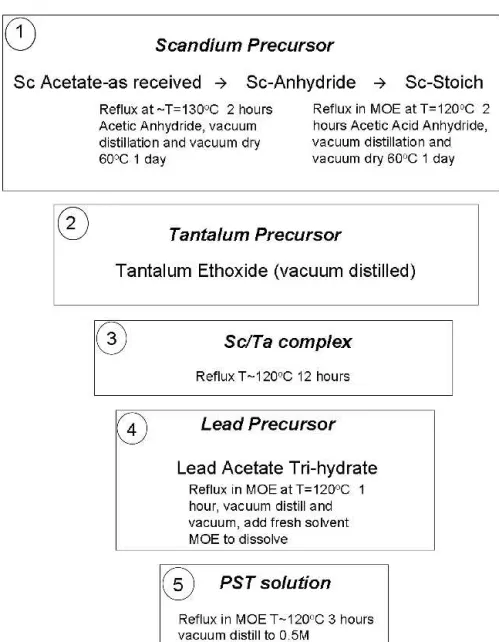
In light of these experiments, an optimized solution synthesis scheme was developed in which (i) the purchased scandium acetate, named “scandium as-received” was first dehydrated with acetic anhydride to form the precursor named “Sc-anhydride” for strict con-trol of material stoichiometry. This Sc-anhydride pre-cursor was subsequently reacted with the solvent MOE resulting in a precursor termed “Stoich”. The Sc-Stoich precursor was characterized by the proper Sc/Ta ratio, as well as enhanced solution stability of the Sc/Ta complex compared with the use of the Sc-anhydride pre-cursor. The Sc-Stoich precursor was then combined with (ii) tantalum ethoxide to form the (iii) Sc/Ta complex. Finally, this B site complex was combined with (iv) lead acetate to obtain the final (v) PST solution. The opti-mized solution synthesis procedure is described graphi-cally in Fig. 4.
IV. FILM FABRICATION EXCESS LEAD
It has been established for many lead containing perovskites fabricated by chemical solution deposition methods that the addition of excess lead is necessary to compensate for surface lead loss as well as interface diffusion in some substrate systems.45This lead loss is not unique to chemical solution derived films, but applies as well to films fabricated from physical deposition methods such as sputtering.29Usually, lead deficiency is accompanied by the appearance of secondary pyrochlore phases, often leading to a fine grain pyrochlore matrix and rosette type perovskite grains.46 Previous reports in the PST system indicate that lead deficiency is also a problem in this material system with additions of up to 20% excess lead being used in some studies.33 Further reports in the PST system indicate that excess lead may also affect the crystallization pathway from amorphous to the final perovskite film.31
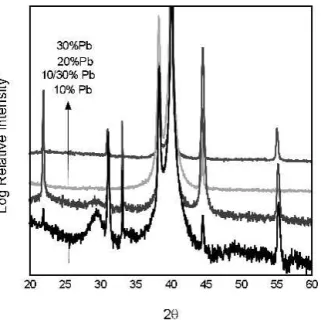
Figure 5 shows the x-ray spectra PST on Pt/Si RTA annealed at 700 °C for 1 min with different excess lead contents; 10%, 10/30% top, 20%, and 30% excess lead in solution. In the case of 10% and 10/30% lead excess combinations, the presence of a pyrochlore phase is seen as indicated by the broad peak at 29°. Samples prepared with 20% and 30% lead excess showed a pure perovskite
TABLE I. EDAX stoichiometry analysis performed on Philips XL-30 SEM for Sc-acetate (as received powders), Sc-Stoich (from MOE process), Sc-isopropoxide and bulk ceramic PST reference (±2%).
Theoretical Ta (L line) Sc (K line) O Sc/Ta
Stoichiometric ratio 10 10 60 1
Sc-acetate (as received) 13.6 7.6 62.5 0.56
Sc-Stoich 8.8 8.6 59.6 0.98
Sc-isopropoxide 8.8 7.4 67.1 0.84
phase according to the x-ray analysis. Although no py-rochlore phase is observed in films with 20% excess lead by SEM or x-ray investigations, the nucleation and growth determined microstructure of the perovskite phase is clearly affected by the lead content. Figure 6 shows TEM diffraction of 10% lead sample indicating that the rosettes are the perovskite phase, surrounded by a polycrystalline matrix exhibiting a face-centered cubic (fcc) diffraction pattern and a lattice parameter of 6.4 Å, typical of lead deficient pyrochlore.
Figure 7(a) compares TEM bright field cross sections of 400 nm films deposited on Pt/Si substrates fabricated from a solution containing 30% excess lead. Columnar grain growth was observed as well as the absence of any secondary pyrochlore phases. The film shows the pres-ence of voids, concentrated especially at the grain bound-ary. However, the concentration of voids is significantly
less than that reported in sputtered PST,8and their posi-tion at the grain boundary lessens their impact on the dielectric response measured “out-of-plane,” where the grain boundary contribution to the capacitance is parallel with the “bulk” film response. Void formation is often observed in the PST system and has been recently attrib-uted to the formation of the intermediate pyrochlore phase, which forms before arriving at the final perovskite phase.31
Of particular interest is the compositional profile of lead across the film thickness of the TEM cross sections in Fig. 7(a). The sample with 30% excess lead in solution was annealed at 700 °C for 1 min, which resulted in drastic lead loss from the surface and film/substrate in-terface, whereas the interior of the film remained lead rich. Short duration annealing times thus allow for a loss of lead from the surface, but do not allow time for lead
diffusion in the bulk of the film to take their equilibrium positions. Lead vacancy formation has been observed in PST ceramics and is in agreement with the PST pervos-kite structure showing a large tolerance for lead stoichi-ometry. This behavior is different than what was ob-served in low temperature sputtered PST films made with 20% excess lead and post annealed using RTA where stoichiometric, or slightly lead rich films were ob-served.31
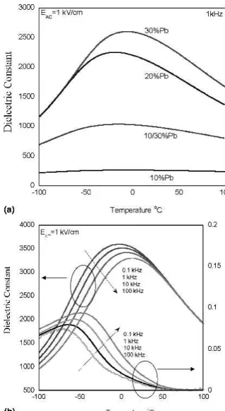
The dielectric properties of the 500 nm films annealed at 700 °C for 1 min fabricated from solutions containing different excess lead concentrations are presented in Fig. 8(a). The reduction of the permittivity in films that contain only 10% lead alone, or in combination with greater excess amounts can be attributed to the presence of a secondary pyrochlore phase. An increase of the per-mittivity with increasing lead concentration is observed, however the difference between the maximum permittiv-ity of films fabricated with 20% and 30% lead is near the uncertainty for the dielectric measurement (∼10%). It is therefore concluded that while these films most probably have differences in the distribution of lead rich and lead deficient regions, the impact on the dielectric response is essentially the same. It was observed that increasing the annealing time to 20 min increased the maximum per-mittivity by 10% with no microstructural changes as ob-served by SEM or structural changes as obob-served by x-ray diffraction. However, it is emphasized that this increase is close to the estimated error for the permittivity due to the uncertainty in both the film thickness and electrode geometry.
Figure 8(b) displays the dielectric constant loss tan-gent as a function of temperature from 100 °C to −100 °C and frequencies from 100 Hz to 100 kHz for a 1.4m PST film prepared from a 30% excess lead solution on a Pt/Si substrate annealed at 700 °C for 20 min. The sample shows a maximum dielectric constant of 3520 at 2 °C and a room temperature loss tangent of 0.8% at 1 kHz. The dielectric constant and the loss tangent
FIG. 5. X-ray diffraction of 500 nm PST films on Pt/Si, RTA annealed in O2to 700 °C for 1 min with 10%, 10/30% combination, 20%, and
30% excess lead in solution.
FIG. 6. Plane view TEM bright field (BF) image and selected area diffraction (SAD) of PST from 10% excess lead solution on Pt/Si substrate annealed at 700 °C 1 min indicating a perovskite “rosette” grain structure in a pyrochlore matrix.
display frequency dispersion characteristics of relaxor behavior. It is also seen in Fig. 8(a) that insufficient levels of excess lead in solution leads to a downward shift in the dielectric maximum along with a reduction in the dielectric constant due to increased levels of a pyro-chlore phase. This is consistent with data on bulk PST relaxors with lead deficiency where a decrease in the temperature of the dielectric maximum is observed with increasing lead vacancy concentration.26,27 A previous study conducted on the thickness dependence of sol-gel derived PST thin films made from solutions containing 20% excess lead showed that the position of the dielectric maximum showed similar values within ±2 °C between films of 300 nm up to 2m.22
From a comparison of Figs. 8(a) and 8(b), a thickness effect is clearly visible. This has been analyzed in detail in Ref. 22 in terms of an interfacial capacitance model concluding that an effective surface layer of 100 nm
thickness and a dielectric constant of 600 may explain this reduction. Microstructural studies in this report pre-sent evidence that this may be due to lead-deficient sur-face layers in series with the bulk capacitance. However, it should be emphasized that even after taking into ac-count an interfacial effect due to lead deficient surface layers, the dielectric constant of the film itself still re-mains small; reduced by an order of magnitude as com-pared to ceramics and single crystal relaxor PST.
V. SUBSTRATE EFFECTS
A number of different substrates were used for PST thin film fabrication in this study. The substrates influ-ence the film through (i) their facility for nucleation and
FIG. 7. (a) TEM bright field (BF) image of film cross sections PST on Pt/Si substrates RTA annealed at 700 °C 1 min from solution contain-ing 30% excess lead. (b) EDX of lead concentration (mol%) as a function of film thickness.
FIG. 8. (a) Dielectric constant at 1 kHz and EAC1 kV/cm of 500 nm
PST films on Pt/Si RTA annealed for 1 min duration in O2atmosphere
made from solutions with 10%, 10/30%, 20%, and 30% excess Pb in solution. (b) 1.4 m thick PST film made from 30% excess lead solution on Pt/Si substrates annealed at 700 °C for 20 min. Dielectric constant and loss tangent versus temperature at EAC1 kV/cm and
growth of the perovskite phase (ii) the induced stress caused by differences in thermal expansion. Solution de-rived films with similar crystal structures as compared to single crystal substrates have been shown to exhibit epi-taxial grain growth. In experiments with conventional ferroelectric PbTiO3derived from chemical solution
pre-cursors, the epitaxial growth mechanism was found to be the same as in polycrystalline samples; an intermediate pyrochlore phase crystallizing from the amorphous pre-cursor followed by epitaxial nucleation of the perovskite phase at the film/substrate interface and growth towards the free surface.47 Chemical solution derived epitaxial thin films of relaxor PMN have been reported on STO substrates49; however, the authors are not aware of any previous report on epitaxial PST thin films using chemi-cal solution deposition.
A. Pt/Si substrates with seed layers
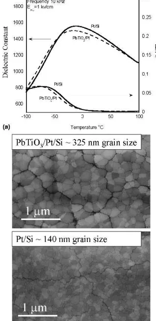
The SEM microstructures of disordered PST thin films fabricated on Pt/Si substrates with and without a PbTiO3
seed layer processed from solutions containing 30% ex-cess lead RTA annealed to 700 °C for 1 min are pre-sented in Fig. 9(a). This seed layer is similar to that used to facilitate PZT crystallization and orientation control in Ref. 48. Similar results with sputter deposited seed layers were obtained for sol-gel derived PMN relaxor thin films.2 PST films in this study deposited directly onto Pt/Si substrates exhibited a (100)/(111) bi-modal grain size distribution, whereas films deposited onto PbTiO3
seed layers showed a pronounced (111) orientation. The grain size is larger in (100)/(111) bi-modal oriented films. This suggests that Pt/Ti substrates used at high temperatures in this study may result in a thin interfacial layer of titania, which impedes heterogeneous nuclea-tion, resulting in fewer nucleation sites and a relatively larger grain size of 325 nm. This is in contrast to the enhanced nucleation of PbTiO3seeded films, which
re-sulted in a fine grain size of less than 140 nm. From the measurements presented in Fig. 9(b) it is seen that no detectable change in the value of the dielectric constant is observed by reducing the grain size from 325–140 nm. B. (100) magnesium oxide (MgO)
Films of PST were deposited on single crystal (100) MgO substrates from solutions containing 30% excess lead resulting in phase pure perovskite with an “out-of-plane” orientation of (100) matching the underlying sub-strate. The x-ray spectra and pole figure of the (110) pole are shown in Fig. 10(a) for a 500 nm PST film RTA annealed to 700 °C for 1 min. The position of the (110) peaks in the inset of Fig. 10(a) indicates an epitaxial relationship with the MgO substrate. The dielectric stant and loss tangent measured in the “In-Plane” con-figuration are presented in Fig. 10(b). The dielectric
maximum for this sample was 1392 at −12 °C and 100 kHz with a room temperature loss tangent of 0.6%. The sample exhibited frequency dispersion typical for relax-ors in the dielectric constant and in the loss tangent. C. (100) and (111) 1% Nb doped strontium titanate (STO)
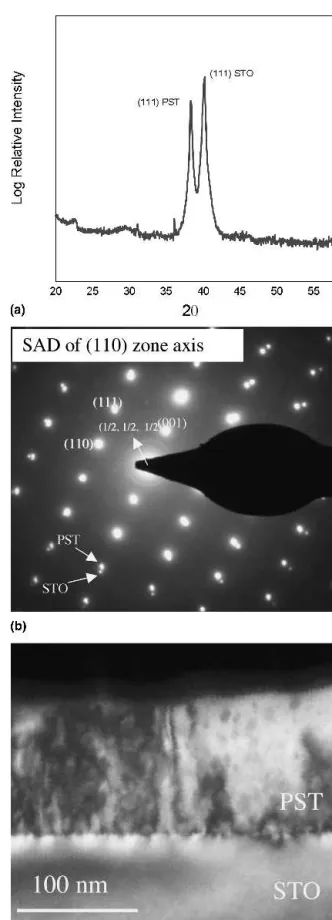
Single crystal (100) and (111) strontium titanate sub-strates doped with 1% Nb were used for the growth of epitaxial (100) and (111) PST films. Figure 11(a) shows the x-ray spectra of (111) PST on (111) STO RTA an-nealed to 700 °C for 1 min indicating phase pure
perov-FIG. 9. (a) Dielectric constant and loss tangent versus temperature for 300 nm PST films on Pt/Si (grain size 140 nm) and PbTiO3(grain size
325 nm) seeded substrates RTA annealed 700 °C 1 min from solutions containing 30% excess lead and (b) SEM images of Pt/Si and PbTiO3
skite and highly oriented films. The epitaxial relationship was also observed in TEM studies of (111) PST as shown in Fig. 11(b). The microstructure of a film as seen by dark field TEM is presented in Fig. 11(c), which shows some porosity in the bulk of the film consistent with previous observations of epitaxial films processed at such low temperatures. The contrast at the film/substrate interface shows evidence of strain induced by lattice mis-match.
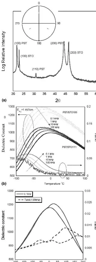
The x-ray spectra of 600 nm PST on STO (100) RTA annealed to 700 °C for 1 min is presented in Fig. 12(a). PST films oriented “out of plane” in the (100) direction were observed, whereas the pole figure of the (111) peak [displayed in the inset of Fig. 12(a)] revealed an
FIG. 11. (a) X-ray spectra of 600 nm PST on STO (111) single crystal substrate RTA annealed at 700 °C 1 min in O2fabricated from
solu-tions containing 30% excess lead. (b) Selected area diffraction (SAD) pattern of 110 zone axis in 111 PST/STO films. (c) TEM dark field (DF) image of 100 nm thick PST on 111 STO substrate.
FIG. 10. (a) X-ray spectra of 500 nm PST on MgO (100) single crystal substrate RTA annealed at 700 °C 1 min in O2. (Inset) Pole figure of
the (110) perovskite peak. (b) Dielectric constant and loss tangent 540 nm PST on MgO measured in the “in-plane” configuration at EAC⳱ 1 kV/cm from 10 kHz to 1 MHz.
“in-plane” orientation, or a global epitaxial relationship between the film and substrate.
Figure 12(b) shows the dielectric constant and loss tangent as a function of temperature from 100 to −100 °C and frequencies from 0.1 to 100 kHz for 600 nm epitaxial PST films on STO (111) and (100) substrates. The film on STO(100) displayed a dielectric constant with a maxi-mum value of 1270 at −18 °C and 1 kHz as compared to 1044 at −16 °C for the (111) oriented sample. The room temperature loss tangent values at 1 kHz are similar at 0.9% for (100) and 0.7% for the (111) oriented speci-mens.
An examination of the CV and PE curves for PST on Nb-doped STO substrates presented in Fig. 12(c) reveals an asymmetry in the response due to the sandwich struc-ture of a metal/ferroelectric/n-type doped semiconductor. As a positive bias is applied to the sample, we see an increase the capacitance, charge and thus the dielectric constant and loss tangent values which reach a maximum at 25 kV/cm applied field before decreasing and exhib-iting a hysteric response as the field is decreased to zero. The internal bias thus applied to our ferroelectric mate-rial is estimated from the displacement of the CV curve to be approximately 25 kV/cm, which can reduce our values of measured dielectric response by up to 10% at temperatures near the dielectric maximum.25A reduction of this magnitude combined with the 10% measurement uncertainty can account for the unusually low values of dielectric response in this work as well as those usually reported for doped STO substrates. Interfacial capaci-tance of the substrate itself was not observed in as-received substrates; however, thermal-induced modifica-tions in the substrate after film annealing were not char-acterized. Therefore, it is possible that interfacial capacitance may pose an additional contribution to the reduced film permittivity on STO substrates.
D. Sapphire
Films were also fabricated on single crystal c-axis ori-ented sapphire substrates. In the case of sapphire, the lattice constant and crystal structure was unfavorable for heterogeneous nucleation at the film/substrate interface and an often detectable amount of pyrochlore was ob-served under the same conditions leading to phase pure perovskite in other substrate/electrode systems. The nu-cleation could be improved by the use of a thin seed layer of sputtered TiO2as previously described for the PZT/
Pt/Si system.48Figure 13(a) shows the x-ray spectra of a 500 nm PST film deposited on sapphire and TiO2/
sapphire and RTA annealed to 700 °C for 20 min. The film without the seed layer displays pyrochlore at 29°, and a random orientation indicative of homogenous nu-cleation in the bulk of the film. The film processed with the aid of a 2 nm TiO2layer indicates phase pure
perov-skite with a high degree of (111) orientation, similar to
FIG. 12. (a) X-ray spectra of 600 nm PST on STO (100) single crystal substrate RTA annealed at 700 °C 1 min in O2fabricated from
solu-tions containing 30% excess lead. (Inset) Pole figure of the (111) perovskite peak. (b) Dielectric constant and loss tangent at 1 kV/cm AC field as a function of frequency from 0.1 kHz to 100 kHz for 100 and 111 oriented PST on Nb doped STO single crystal substrates. (c) Dielectric constant and loss tangent versus DC electric field, or CV curve measurement.
the enhanced (111) PZT nucleation with the use of tita-nia. Figure 13(b) displays a TEM bright field image of PST with TiO2 seed layer displaying large micron size
grains with evidence of some entrapped porosity in the grain interior.
Figure 13(c) displays the dielectric response of a 620 nm film of disordered PST on a sapphire substrate annealed at 700 °C for 20 min. The dielectric maximum of 2110 occurs at 10 °C at 100 kHz, with a paraelectric phase loss tangent at 50 °C of 1.2%. Differences are seen as to the position of the dielectric maximum of films on MgO or sapphire substrates, with a higher temperature of the dielectric maximum occurring for films on sapphire. VI. DISCUSSION
Optimized solution processing led to phase pure per-voskite PST in the disordered state exhibiting relaxor ferroelectric behavior on a number of different substrate systems including Pt/Si, MgO, sapphire, and STO. All the polycrystalline and epitaxial films fabricated in this study exhibited a drastically reduced dielectric constant maximum compared with ceramics. In addition, the use of seed layers to tailor the grain size showed that dou-bling the grain size from 140 nm to 325 nm on Pt/Si substrates had a negligible effect on the permittivity. Epi-taxial films and films with large grain sizes in the micron regime also exhibited low permittivity. Although a grain size effect on the permittivity was not observed, the choice of substrate was seen to have a large impact on the position of the dielectric maximum. In the following sec-tion we present the impact of thermal induced stress on the dielectric response of thin film relaxor PST.
This thermal stress can be expressed in Eq. (1) where X is the stress, Ef andf are the Young’s modulus and
Poisson’s ratio of the film, and ⌬T is the temperature difference between the crystallization temperature and the final film temperature after cooling. For␣s<␣fthe
film will be under tension (as is the case for PST on Si). X= Ef
1− f
共␣f − ␣s兲⌬T . (1)
In epitaxial films on MgO, the in plane lattice param-eter a||was directly measured using grazing angle x-ray
measurement and the stress state of the film was esti-mated using Eqs. (2) and (3).
x =a||− ao
ao . (2)
<
FIG. 13. (a) X-ray spectra of 500 nm PST from solutions containing 30% excess lead on single crystal sapphire substrates (0001) RTA annealed at 700 °C 20 min with and without a sputter deposited 2 nm TiO2seed layer. (b) TEM BF image of PST on TiO2seeded sapphire
substrate annealed at 700 °C 20 min. (c) Dielectric constant and loss tangent for 620 nm PST on sapphire at EAC⳱1 kV/cm from 10 kHz to
Where x is the strain, a is the mechanically free lattice parameter, and a|| is the experimentally measured
in-plane lattice constant
X= Efx . (3)
Table II presents the thermal expansion data for PST and the substrates used in this study along with the calculated stress in the film upon cooling from 700 °C calculated using Eq. (1). The calculated stress is compared with the measured stress on two substrate systems as verification of our assumption that thermal stress dominates in nomi-nally thick films.
A wafer bending technique was used to examine the stress in PST films on Pt/Si substrates resulting in a measured stress of 700 MPa in tension, significantly greater than the estimated stress level of near 370 MPa. However, this analysis is complicated by the presence of the Pt electrode which also exhibits thermal stress and may account for the observed discrepancy in the present case. Film stress determined from measurements of the “in-plane” lattice parameter indicated a compressive stress of 180 MPa as compared with the calculated value of 640 MPa. This apparent underestimate of the film stress may be due to the measurement technique, which preferentially samples the surface layers that are ex-pected to be less strained than the near-by electrode lay-ers, thus skewing the data to lower stress levels.
Overall it is important to note that the sign of the calculated and measured stress is the same, so that we may use the calculated stress levels to compare, in gen-eral, films that are in tension versus compression. This data is consistent with the literature on thin film relaxors, which states that the film stress state in nominally thick films is dominated by thermal expansion and not inter-facial strain.
Figure 14(a) displays the temperature of the dielectric maximum at 10 kHz versus the calculated stress (MPa) induced by thermal expansion mismatch summarized in Table II. All films were fabricated from solutions con-taining 30% excess lead and were annealed at 700 °C for
1 min. Although the thickness of the films in the present case varies by ∼100 nm, this may be assumed to be negligible for the present discussion. Indicated on the graph is the position of the dielectric maximum at 10 kHz for disordered ceramic relaxor PST (PST-D) and disor-dered ceramic relaxor PST with lead vacancies (PST-DV) taken from Ref. 27 showing that the presence of vacancies/defects reduces the temperature of the dielec-tric maximum.
In light of these factors, the differences in the position of the dielectric maximum are attributed to substrate ef-fects, specifically the stress/strain induced from the thermal expansion mismatch upon cooling from the crystallization temperature. It is seen that PST film on sapphire that has the least thermal induced stress has its dielectric maximum position equivalent with the bulk ceramic samples with lead vacancies (PST-DV). As the substrate is changed and stress levels move into
TABLE II. PST and Substrate Thermal Expansion and Stress Data: Calculated stress determined from Eq. (1) with Ef⳱ 1 × 10
11N/m2 andf⳱ 0.3. Material TEC␣ × 10−6K−1 Calculated stress MPa Eq. (1) Measured stress MPa PST 6.5 Si 4 +370 (tension) +700 (tension)a STO 11.7 −380 (compression)
MgO 13.6 −640 (compression) −180 (compression)b Al2O3(sapphire) 6.7 −20 (compression)
aStress measured using wafer bending technique upon cooling from crys-tallization temperature.
bIn-plane lattice parameter measured by grazing angle x-ray a
||⳱ 4.068 Å, and mechanically free a⳱ 4.075 Å.
FIG. 14. (a) Stress effect on the position of the dielectric maximum at 10 kHz and 1 kV/cm AC. (b) Stress effect on the value of the dielectric maximum at 10 kHz.
compression or tension, the temperature of the dielectric maximum decreases. These observations are in agree-ment with Ref. 37 where PMN-PT films showed a de-crease in the temperature of the dielectric maximum un-der both tensile and compressive stresses.
Through control of the stress state of thin film relax-ors, Fig. 14(a) shows that position of the dielectric maxi-mum of thin films can approach that of bulk ceramics. However, Fig. 14(b) displaying the value of the dielectric constant maximum as a function of thin films stress shows that the dielectric constant of relaxor thin films are reduced by an order of magnitude regardless of the stress state. These results suggest that the origin of the reduction of thin film permittivity is not a simple func-tion of mechanical constraint of the film by the substrate. Although it is emphasized that in relaxor materials, the relation between strain/stress and the dynamics of polar nanoregions is far from being understood.
Given the evidence presented in this study it is pos-sible that microstructural features are responpos-sible for the low thin films dielectric constant. Studies by Ostap-chuk50 have pointed out the impact of microstructural features such as voids and cracks and shown that such defects could be responsible for a reduction in the per-mittivity at low frequencies, as well as a harder soft mode and lower dielectric response at high frequencies. In ad-dition, the low temperature of thin film processing may also lead to an incomplete transformation into the relaxor state.22 This is to say that the disordered state of PST relaxor thin films processed at 700 °C, although nomi-nally the same when characterized by x-ray diffraction studies, may in fact be different than the disordered state of PST ceramics processed at high temperatures near 1500 °C. This may lead to a composite of relaxor regions and “underdeveloped” relaxor regions thus reducing the dielectric response.
VII. CONCLUSION
An optimized solution synthesis procedure was used to fabricate phase pure PST thin films. It was found that excess lead in solution in quantities of up to 30% was required for pure perovskite phase development. Epi-taxial films were observed on STO and MgO single crys-tal substrates, the first known results of this nature for sol-gel derived PST relaxor thin films. The effect of thin film stress on the dielectric properties was a downward shift in the temperature of the dielectric maximum for films under both compressive and tensile stress. How-ever, the values of the film’s dielectric maxima were reduced by an order of magnitude as compared to ceram-ics, regardless of the stress state of the film. Mechanical stress alone is therefore not the sole factor in the com-monly observed reduction of permittivity in PST relaxor thin films.
ACKNOWLEDGMENTS
We acknowledge the Swiss National Science Founda-tion for funding and the COST 525 European AcFounda-tion as well as Raymond Houriet [Ecole Polytechnique Fédérale de Lausanne (EPFL)], Stephen Parola, Lyon France, Z. Kighelman, D. Damjanovic, P. Muralt, and Bong-Jin Kuh [Korea Advanced Institute of Science and Technol-ogy (KAIST)] for helpful discussions.
REFERENCES
1. S-E. Park and T.S. Shrout: Ultrahigh strain and piezoelectric be-havior in relaxor based ferroelectric single crystals. J. Appl. Phys.
82,1804 (1997).
2. Z. Kighelman, D. Damjanovic, and N. Setter: Electromechanical properties and self-polarization in relaxor Pb(Mg1/3Nb2/3)O3thin
films. J. Appl. Phys. 89, 1393 (2001).
3. L. Francis, Y. Oh, and D. Payne: Sol-gel processing and properties of lead magnesium niobate powders and thin-layers. J. Mater. Sci.
25,5007 (1990).
4. J. Park and S. Trolier-McKinstry: Dependence of dielectric and piezoelectric properties on film thickness for highly 100-oriented lead magnesium niobate-lead titanate (70/30) thin films. J. Mater.
Res. 16, 268 (2001).
5. B.J. Kuh, W.K. Choo, K. Brinkman, D. Damjanovic, and N. Setter: Dielectric and piezoelectric properties of relaxor Pb(Sc1/2Nb1/2)O3thin films. Appl. Phys. Lett. 83, 1614 (2003).
6. M. Tyunina and J. Levoska: Dielectric nonlinearity in relaxor and ferroelectric thin films of chemically ordered PbSc0.5Nb0.5O3. Appl. Phys. Lett. 85, 4720 (2004).
7. D. Liu and D. Payne: Lower temperature crystallization and or-dering in sol-gel derived Pb(Sc0.5Ta0.5)O3 powders and
thin-layers. J. Appl. Phys. 77, 3361 (1995).
8. Z. Huang, P. Donohue, Q. Zhang, D. Williams, C. Anthony, M. Todd, and R. Whatmore: Comparative studies of PST thin films as prepared by sol-gel, LDCVD and sputtering techniques.
Integrated Ferroelectrics 45, 79 (2002).
9. K. Brinkman, M. Cantoni, A. Tagantsev, P. Muralt, and N. Setter: Dielectric response and structural features of Pb(Sc1/2Ta1/2)O3
(PST) sol-gel derived thin films. J. Electroceram. 13, 105 (2004). 10. S. Kamba, M. Berta, M. Kempa, J. Petzelt, K. Brinkman, and N. Setter: Far-infrared soft-mode behavior in Pb(Sc1/2Ta1/2)O3
thin films. J. Appl. Phys. 98, 074103 (2005).
11. S. Kamba, M. Kempa, V. Bovtun, J. Petzelt, K. Brinkman, and N. Setter: Soft and central mode behaviour in Pb(Mg1/3Nb2/3)O3
relaxor ferroelectric. J. Phys.: Condens. Matter 17, 3965 (2005). 12. R. Ramesh, S. Aggarwa, and O. Auciello: Science and technology of ferroelectric films and heterostructures for non-volatile ferro-electric memories. Mater. Sci. Eng. 32, 191 (2001).
13. B. Nagaraj, S. Aggarwal, T.K. Song, T. Sawhney, and R. Ramesh: Leakage current mechanisms in lead-based thin film ferroelectric capacitors. Phys. Rev. B 59, 16022 (1999).
14. M. Dawber, K. Rabe, and J. Scott: Physics of thin-film ferroelec-tric oxides. Rev. Mod. Phys. 77, 1083 (2005).
15. X. Ren: Large electric-field-induced strain in ferroelectric crystals by point-defect-mediated reversible domain switching. Nat.
Mater. 3, 91 (2004).
16. B. Li, G. Li, Q. Yin, Z. Zhu, A. Ding, and W. Cao: Pinning and depinning mechanism of defect dipoles in PMN-PZT ceramics.
J. Phys. D: Appl. Phys. 38, 1107 (2005).
17. A. Agronin, Y. Rosenwaks, and G. Rosenman: Direct observation of pinning centers in ferroelectrics. Appl. Phys. Lett. 88, 072911 (2006).
18. R. Schwartz, J. Voigt, B. Tuttle, D. Payne, T. Reichert, and R. DaSalla: Comments on the effects of solution precursor char-acteristics and thermal processing conditions on the crystallization behavior of sol-gel derived lead zirconate titanate thin films.
J. Mater. Res. 12, 444 (1997).
19. J. Chang and S. Desu: Effects of dopants in PZT films. J. Mater.
Res. 9, 955 (1994).
20. R.W. Whatmore, A. Patel, N. Shorrocks, and F.W. Ainger: Fer-roelectric materials for thermal IR sensors state-of the-art and perspectives. Ferroelectrics 104, 269 (1990).
21. A. Bratkovsky and A. Levanyuk: Smearing of phase transition due to a surface or a bulk inhomogeneity in ferroelectric nanostruc-tures. Phys. Rev. Lett. 94, 107601 (2005).
22. K. Brinkman, V. Cherman, D. Su, A. Tagantsev, and N. Setter: In-plane versus out-of-plane dielectric response in the thin-film relaxor Pb(Sc1/2Ta1/2)O3. Phys. Rev. B 73, 214112 (2006).
23. C. Stenger and A. Burggraaf: Order-disorder reactions in the fer-roelectric perovskites Pb(Sc1/2Ta1/2)O3and Pb(Sc1/2Nb1/2)O3
ki-netics of the ordering process. Phys. Status Solidi 61, 275 (1980). 24. N. Setter and E. Cross: The role of B-site cation disorder in diffuse phase-transition behavior of perovskite ferroelectrics. J. Appl.
Phys. 51, 4356 (1980).
25. K. Brinkman, A. Tagantsev, P. Muralt, and N. Setter: Self-polarization in Pb(Sc1/2Ta1/2)O3thin films: Impact on dielectric
and piezoelectric response. Jpn. J. Appl. Phys. 45, 7288 (2006). 26. F. Chu: The ferroelectric phase transition in complex perkovskite
relaxors. Ph.D. Thesis, Swiss Federal Institute of Technology EPFL, Lausanne, Switzerland (1994).
27. F. Chu, N. Setter, and A. Tagantsev: The spontaneous relaxor-ferroelectric transition of Pb(Sc1/2Ta1/2)O3. J. Appl. Phys. 74,
5129 (1993).
28. I. Reaney, D. Barber, and R. Watton: TEM studies of rf magnetron-sputtered thin films. J. Mater. Sci.-Mater. Electron. 3, 51 (1992).
29. R. Whatmore, Z. Huang, and M. Todd: Sputtered lead scandium tantalate thin films: Pb+4 in B sites in the perovskite structure. J. Appl. Phys. 82, 5686 (1997).
30. C. Bjormander, K. Sreenivas, A. Grishin, and K. Rao: Pyroelectric Pb(Sc0.5Ta0.5)O3/Y1Ba2Cu3O7−xthin film heterostructures. Appl. Phys. Lett. 67, 58 (1995).
31. Z. Huang, J. Battat, P. Donohue, M.A. Todd, and R.W. Whatmore: On the phase transformation kinetics in lead scandium tantalate thin films. J. Phys. D: Appl. Phys. 36, 3039 (2003).
32. R. Whatmore, A. Patel, and N. Shorrocks: Physicochemical prop-erties of sol-gel derived lead scandium tantalate Pb(Sc0.5Ta0.5)O3
thin-films. Ferroelectrics 134, 343 (1992).
33. D. Liu and D. Payne: Lower temperature crystallization and or-dering in sol-gel derived Pb(Sc0.5Ta0.5)O3powders and thin
lay-ers. J. Appl. Phys. 77, 3361 (1995).
34. V. Fuflyigin, E. Salley, P. Vakhutinsky, A. Osinsky, J. Zhao, I. Gergis, and K. Whiteaker: Freestanding films of Pb(Sc0.5Ta0.5)O3for
un-cooled infrared detectors. Appl. Phys. Lett. 78, 365 (2001). 35. N.A. Pertsev, A.G. Zembilgotov, and A.K. Tagantsev: Effect of
mechanical boundary conditions on phase diagrams of epitaxial ferroelectric thin films. Phys. Rev. Lett. 80, 1988 (1998). 36. V. Nagarajan, S. Alpay, C. Ganpule, B. Nagaraj, S. Aggarwal,
E. Williams, A. Roytburd, and R. Ramesh: Role of substrate on the dielectric and piezoelectric behavior of epitaxial lead magne-sium niobate-lead titanate relaxor thin films. Appl. Phys. Lett. 77, 438 (2000).
37. G. Catalan, M. Corbett, R. Bowman, and J. Gregg: Effect of thermal expansion mismatch on the dielectric peak temperature of thin film relaxors. J. Appl. Phys. 91, 2295 (2002).
38. A. Seifert, N. Ledermann, S. Hiboux, J. Baborowski, P. Muralt, and N. Setter: Processing optimization of solution derived Pb(Zr1−xTix)O3 thin films for piezoelectric applications. Inte-grated Ferroelectrics 35, 1889 (2001).
39. P.K. Petrov, K. Sarma, and N.M. Alford: Evaluation of residual stress in thin ferroelectric films using grazing incident x-ray dif-fraction. Integrated Ferroelectrics 63, 695 (2004).
40. O. Vendik, S. Zubko, and M. Nikolski: Modeling and calculation of the capacitance of a planar capacitor containing a ferroelectric thin film. Tech. Phys. 44, 349 (1999).
41. S. Parola, R. Khem, D. Cornu, F. Chassagneux, S. Lecocq, Z. Kighelman, and N. Setter: Insights in the sol-gel processing of Pb(Mg1/3Nb2/3)O3. The synthesis and crown structure of a new
lead magnesium cluster: Pb6Mg12(-OAc)6(2,n 2 -OAc)18(3, n 2 -OC2H4OPr i
)12. Inorg. Chem. Commun. 5, 316 (2002).
42. B. Malic, M. Kosec, I. Arcon, and A. Kodre: Homogeneity issues in chemical solution deposition of Pb(Zr,Ti)O3thin films. J. Eur. Ceram. Soc. 25, 2241 (2005).
43. D. Liu, L. Ma, D. Payne, and D. Viehland: Sol-gel synthesis of Pb(Sc0.5Ta0.5)O3powders and thin-layers. Mater. Lett. 17, 319
(1993).
44. B. Malic, I. Arcon, A. Kodre, and M. Kosec: EXAFS study of amorphous precursors for Pb(Zr,Ti)O3ceramics. J. Sol.-Gel Sci. Technol. 16, 135 (1999).
45. B. Malic, M. Kosec, K. Smolej, and S. Stavber: Effect of precur-sor type on the microstructure of PbTiO3 thin films. J. Eur. Ceram. Soc. 19, 1345 (1999).
46. T. Boyle, D. Dimos, R. Schwartz, T. Alam, M. Sinclair, and C. Bucheit: Aging characteristics of a hybrid sol-gel Pb(Zr,Ti)O3
precursor solution. J. Mater. Res. 12, 1022 (1997).
47. A. Seifert, F. Lange, and J. Speck: Epitaxial-growth of PbTiO3
thin films on (001) SrTiO3from solution precursors. J. Mater. Res. 10, 680 (1995).
48. P. Muralt, T. Maeder, L. Sagalowicz, S. Hiboux, S. Scalese, D. Naumovic, R. Agostino, N. Xanthopoulos, H. Mathieu, L. Patthey, and E. Bullock: Texture control of PbTiO3and Pb(Zr,Ti)O3thin
films with TiO2seeding. J. Appl. Phys. 83, 3835 (1998).
49. Z. Kighelman: Ph.D. Thesis. Swiss Federal Institute of Technol-ogy EPFL, Lausanne, Switzerland (2001).
50. T. Ostapchuk, J. Petzelt, V. Zelezny, A. Pashkin, J. Pokorny, I. Drbohlav, R. Kuzel, D. Rafaja, B. Gorshunov, M. Dressel, C. Ohly, S. Hoffman-Eifert, and R. Waser: Origin of soft-mode stiffening and reduced dielectric response in SrTiO3thin films. Phys. Rev. B 66, 235406 (2002).