• Aucun résultat trouvé

Dual-Input Switched Capacitor Converter Suitable for Wide Voltage gain Range

N/A
N/A
Protected

Academic year: 2021

Partager "Dual-Input Switched Capacitor Converter Suitable for Wide Voltage gain Range"

Copied!
9
0
0

Texte intégral

(1)

HAL Id: hal-01217668

https://hal.archives-ouvertes.fr/hal-01217668

Submitted on 21 Oct 2015

HAL is a multi-disciplinary open access

archive for the deposit and dissemination of

sci-entific research documents, whether they are

pub-lished or not. The documents may come from

teaching and research institutions in France or

abroad, or from public or private research centers.

L’archive ouverte pluridisciplinaire HAL, est

destinée au dépôt et à la diffusion de documents

scientifiques de niveau recherche, publiés ou non,

émanant des établissements d’enseignement et de

recherche français ou étrangers, des laboratoires

publics ou privés.

Dual-Input Switched Capacitor Converter Suitable for

Wide Voltage gain Range

Gaël Pillonnet, Arnaud Andrieux, Elad Alon

To cite this version:

Gaël Pillonnet, Arnaud Andrieux, Elad Alon. Dual-Input Switched Capacitor Converter Suitable for

Wide Voltage gain Range. IEEE Journal on Emerging and Selected Topics in Circuits and Systems,

IEEE, 2015, �10.1109/JETCAS.2015.2462014�. �hal-01217668�

(2)

Copyright (c) 2015

Abstract — The capacitive-based switching converter suffers

from low efficiency, except for a few conversion ratios, thus limiting its use in fine dynamic voltage and frequency scaling for the power management of digital circuits. Therefore, this paper proposes a Multiple Input Single Output Switched Capacitor Converter (MISO-CSC) to provide flatness efficiency over a large voltage gain range. First, the power efficiency calculation in MISO configuration is given, and then the best ones to optimize the number of switched capacitor structures is selected. By using two power supplies, the MISO converter produces 18 ratios instead of three in SISO (Single Input Single Output) mode. Using a CMOS 65nm technology, the transistor-based simulations exhibit an average 15% efficiency gain over a 0.5-1.4V output voltage range compared to the SISO-CSC.

Index Terms— switched capacitor converter, multi-input

converter, power efficiency optimization, fully integrated voltage regulator, dynamic voltage and frequency scaling.

I. INTRODUCTION

VER (IN) the last decade, electrical portable devices such as the mobile phone have transformed from having a simple display and basic capability into complex computers. The run time of these portable devices is increasingly difficult to maintain as they become more feature-rich. Today, the relative stability of energy storage requires an efficient control of battery power. Furthermore, with the move to parallelism and heterogeneity, there is a clear need to support multiple independent supply voltages on the same digital IC [1]. However, at the present time, it is not feasible to support the number of required supplies in a tiny PCB with a large number of external power converters and their associated passive components [2].

Power management has also been moving away from external power modules towards on-chip or in-package solutions [2]. While the inductive switching converter (ISC) is currently the most popular solution for board-level power management, previous studies have predicted that this topology is no longer suitable for on-chip power management [3]. The significant potential of the switched-capacitor

Manuscript received October X, 20XX. This work was supported by the Commissariat à l’Energie Atomique et aux Energies Alternatives (CEA).

G. Pillonnet and A. Andrieu are with Univ. Grenoble Alpes, F-38000 Grenoble, France, and CEA, LETI, MINATEC Campus, F-38054 Grenoble, France (e-mail: gael.pillonnet@cea.fr).

A. Andrieu is also with INSA Lyon, Villeurbanne, France.

E. Alon is are with the Department of Electrical Engineering and Computer Sciences, University of California at Berkeley, Berkeley, CA 94704 USA (e-mail: elad@eecs.berkeley.edu).

converter is largely addressed in the literature for a fully-integrated supply [4]. Recent work proved that the capacitor-based converter achieves high efficiency in a small die area [5-7, 9]. However, the optimal efficiency is only reached for some given conversion ratios. The converter acts as a low-efficiency linear regulator outside these ratios. Considering an ideal switch, Figure 1 shows the theoretical efficiency achieved by the ISC and the Switching Capacitor Converter (CSC) in a 2:1 configuration over the conversion range (defined by output to input voltage ratio Vout/Vin). The CSC

suffers from a fundamental efficiency limit outside its own ratio (1/2 in this example). On the other hand, the ISC maintains an ideal efficiency. Conversion ratio control is done by modulating the switching frequency in the CSC, duty cycle in ISC.

Fig. 1. Theoretical efficiency limit vs conversion ratio (Vin/Vout) for step-down

Inductive (ISC) and Capacitive (CSC) Switching Converters.

A wide range of conversion ratio is needed in some applications such as the processor supply in a battery-powered application [5, 8]. In fact, the input converter voltage largely varies depending on the battery status and power consumption of the surrounding circuits. Dynamic voltage scaling in digital circuits also requires a wide converter output voltage range. A converter producing a large ratio range is therefore required but the optimal efficiency of a CSC is rarely achieved [2].

To address the above limitation, some papers propose reconfigurable topologies [3, 12] or double outputs [11] to optimize efficiency for multiple conversion ratios. However, the converter still acts outside the few added ratios proposed in the literature in most applications [5]. Another solution is to design a hybrid structure using switched capacitor connected in series to a magnetic converter [15]. The authors of [16] obtained a better efficiency over a wider range even though the inductor was less constrained than in a classical pure inductive converter; its integration on chip in hybrid architecture would still be challenging for some applications.

Dual-Input Switched Capacitor Converter

Suitable for Wide Voltage gain Range

Gaël Pillonnet, Arnaud Andrieu, and Elad Alon

(3)

2 This paper presents a novel topology to overcome the

efficiency limitation in the pure capacitive-based converter. The authors propose powering the converter by multi-power supplies, i.e. Multi-Input Single-Output CSCs (MISO-CSCs) as shown in Figure 2. Despite the extra input rails, i.e. potentially leading to additional external converters, this paper quantifies the efficiency gain by using two inputs instead of one. We then propose an alternative approach to improve the efficiency in the fully-integrated power converter by moving the constraint to the less challenging external DC-DC converter. A MISO has already been proposed in [17] but concerns the ISC, not the capacitive one. A MIMO has been introduced in [18] but its use and constraints are far from the focus of this paper.

Fig. 2. SISO-CSC and MISO-CSC architecture.

Section 2 introduces the additional capabilities of the powered converter with series-parallel connection of multi-flying capacitors. Based on a previous study [14], Section 3 describes the method to calculate power efficiency in the MISO-CSC. Section 4 selects the relevant ratios to propose the simplest reconfigurable topology based on two power supplies. Based on transistor-level simulation, the authors compare the efficiency of the single- and multi-powered on-die converters to provide a larger conversion ratio range in the context of the granular power supply. Lastly, the authors discuss the global power distribution strategy using an MISO-CSC including the extra external converter to provide the additional input voltage.

II. SINGLE- AND MULTI-INPUT CSC

A. SISO limitation to generate constant efficiency

When the switching converter is powered by one power supply (SISO), the number of efficient conversion ratios is limited. Figure 3 shows all possible converter connections with one flying capacitor and two phases (ϕ1,2). The upper and

lower terminals can be connected to the input voltage Vin,

output voltage Vout or ground. At each phase, there are 9

connection possibilities for the flying capacitor. Thus, there are 81 different configurations (9 times 9) with two-phase converter operation (capacitor connected to two voltages in the first phase followed by another phase connected to two other voltages). Each possibility generates a maximal efficiency at a specific conversion ratio (defined by α=Vout/Vin).

The following example presents how to calculate the 1/2 ratio configuration considering ideal switches, steady-state condition, no load and constant output voltage. In this configuration, the upper terminal is connected to Vin in ϕ1 and

Vout in ϕ2. The lower terminal is connected to Vout in ϕ1 and

ground in ϕ2. The input and output energies (Ein,i, Eout,i) in

phase i provided during one period (two phases) are equal to:

out out in in in in in in QV QV E E E QV E E             2 , 1 , 1 , (1)

where ΔQ = Q1-Q2, Qi is the flying capacitor charge during the

ith phase, and Ex,i is the energy given or received during the ith

phase.

Fig. 3. Possible connections for the flying capacitor in SISO-CSC.

To obtain 100% efficiency, the input energy must be equal to the output energy. In this example, the conversion ratio is fixed at 1/2: 2 1 in out out in V V E E        (2)

By using the same method for each of the 81 possible configurations, only 4 ratios with ideal power efficiency, α, can be obtained:        ;1;2 2 1 ; 1

(3)

Therefore, the switching converter with one flying capacitor has only one optimal ratio in “step down” condition (0<α<1). Outside this ratio, the CSC acts as a linear regulator leading to low efficiency.

B. Series-parallel connection to add more ratios

To increase the number of optimal conversion ratios, previous work [5-7] proposes to partition the flying capacitor into multi-standard cells. Figure 4 shows the case with two equivalent cells. Now, there are 2×81 different configurations for two phases:

 81 with Cfly in ϕ1 and Cfly in ϕ2 (as one flying

capacitor)

 81 with Cfly in ϕ1 and Cfly/2 in ϕ2 (or inversely)

For example, the 2/3 configuration has the same flying capacitor terminal connection as the 1/2 configuration, but the equivalent capacitor value is Cfly in ϕ1 and Cfly/2 in ϕ2. The

lower terminal is connected to Vout in ϕ1 and ground in ϕ2. The

energy can be expressed as:

1 2 1 2 1 2 1 Q Q V Q V Q Q E V Q Q E out out out in in           (4)

where ΔQn=Qn,1-Qn,2 and Qn,i is the charge of the nth flying

(4)

Fig. 4. 24 possible configurations for two flying capacitors in SISO-CSC.

This configuration allows generation of a 2/3 conversion ratio without charging loss:

Ein Eout Vout Vin 3 2 1      (5)

Using the same method, the generated ratios of the 162 possible configurations are as follows:

       ;2;3 2 3 ; 1 ; 3 2 ; 2 1 ; 3 1 ; 3 1 ; 2 1 ; 3 2 ; 1 ; 2

(6)

Flying capacitor partitioning is therefore a relevant technique to increase the number of optimal ratios in “step down” condition. Now, there are 3 ratios {1/3; 1/2; 2/3} compared to one with one flying capacitor {1/2}. However, this is not sufficient to obtain high efficiency over a wide conversion ratio range.

The partitioning technique could be used with more than two flying capacitors. Table 1 summarizes the number of optimal conversions obtained with 1, 2 and 3 cells. Increasing the cell number improves the overall efficiency but the constraints on the switches increase (voltage drive, bulk connection, on/off driving). The multiple cell technique (more than 2 cells) could thus be difficult to implement [6].

TABLEI

NUMBER OF OPTIMAL RATIOS USING THE PARTITIONING TECHNIQUE (1 INPUT) # flying cell # optimal ratios (where η=1) # optimal ratios in step-down conversion (0<α<1) 1 4 1 2 7 3 3 16 7

C. MISO associated with series-parallel connection

By adding more input power supplies, the lower and upper terminals of the flying capacitor could be connected to other voltages at each phase. Then, the number of configurations would be increased to generate optimal conversion ratios. For example, Figure 5 shows the potential connection with N power supplies {Vin, Vin2, …, VinN} and one flying capacitor

Cfly. Here, there are (N+2)2 possibilities to connect the flying

capacitor at each phase. The topology leads to (N+2)4

configurations in two phases. This method extends the number of possibilities more than by adding one more flying capacitor.

Fig. 5. (N+2)4 possible configurations for MISO-CSC.

Table 2 summarizes the number of maximal optimal ratios in step-down configurations (0<α<1) by using two or three power supplies. The results are extracted by following the method described in Section II.A. We observe that the number of optimal step-down ratios depends on the values of the input power supplies.

TABLEII

NUMBER OF OPTIMAL STEP-DOWN RATIOS USING THE MULTI-POWERED TECHNIQUE

# input power supply

# maximal optimal ratio with 1 flying cap.

# maximal optimal ratio with 2 flying cap.

1 1 3

2 6 18

3 17 27

The number of optimal ratios dramatically increases with the number of input power supplies, potentially leading to more constant power efficiency over conversion ratio. Adding only one input leads to 15 more ratios. In the following section, we chose to study the dual input CSC by considering the added ratio benefit versus the extra converter needed to generate inputs.

III. POWER EFFICIENCY OF MULTI-POWERED CSC As in the capacitor partitioning technique (Section II.C), the extra generated ratios do not have the same efficiency to transfer the energy from the inputs to the output. This section therefore introduces a general expression of power efficiency for multi-powered CSCs.

Previous work [14] studied the loss mechanism in the CSC in detail. Here, the same analysis is used but is extended to N inputs.

A. Method to model losses in a capacitive-based converter

Seeman [14] developed a method to fully determine the steady-state performance of CSCs using only three parameters: Msw, Mcap, Mbot. These correspond to the

conduction loss Pcond, energy transfer loss Pcfly, and bottom

plate loss Pbott, respectively. From [14], the total power loss

can be expressed as:

2 2 2 1 sw sw c sw fly bott sw fly o cap o r sw sw bott cfly cond losses V Wf f C M f C I M I W M P P P P P

        (7) where Psw is the switching loss, Cfly the total flying capacitor

value, W the total width of the switches, λr the on-state

resistance density measured in Ω·m, λc the gate capacitance

(5)

4 capacitor ratio, fsw the switching frequency, and Vsw the

voltage swing to drive the switch gates. The power efficiency is given by:

sw cfly

losses o o

f

W

f

C

P

P

P

,

,

(8) where Po = Vo·Io.

The efficiency could be maximized by varying the three design freedom parameters {W, fsw, Cfly}. The other

parameters {λi, θ} and {Mi} only depend on silicon

technology and configuration, respectively. In area-driven optimization, Cfly is maximized to obtain the highest

efficiency.

The authors of [12] proved that the efficiency at high power density is directly linked to Msw/Mcap and is equal to (i.e. SSL

hypothesis [14]): 3 2 2 3

3

fly o c r o sw cap sw o losses

C

R

V

V

M

M

P

P

(9) where Ro is the load resistor.

So, if a configuration exhibits a low Msw and a high Mcap, its

efficiency will be suitable for highly efficient conversion.

B. Calculation example for one configuration

Figure 6 shows one particular configuration generated by using two input power supplies and two flying capacitors.

Fig. 6. (2+β)/3 configuration with two inputs and two flying capacitors in MISO-CSC.

In steady-state, the conversion ratio is given by:

3

2

i o

V

V

(10) where β=Vin/Vin2

Using Seeman’s method, the three parameters can be calculated as follows:

2 2 , 3 1 4 3 2 3 2 2          

ri sw a M (11)

2 2 ,

3

1

2

1

1

 

ci cap

a

M

(12)

2

1

2

5

2 bott

M

(13) where ax,y follows the notation presented in [14].

C. Results for all step-down conversion ratios

The appendix gives the three parameters for all configurations which generate a step-down conversion ratio (0<α<1) for any β.

The 1/2 and similar (β /2, (1+β)/2) ratios are the most efficient (low Msw, high Mcap). The extra ratios generated by

positive combination of the two inputs have parameters similar to those of the mono-powered converter. It would therefore be the best candidate to generate efficient ratios. Moreover, the input combination with a minus operator (e.g. 1-β) achieves high Msw (high conduction loss) potentially

leading to low efficiency conversion. IV. TWO INPUT CSC

The analysis above gives the analytical equations to calculate and optimize the power efficiency at each ratio. In this section, the optimal design parameters {Wsw, fsw} are

given for a particular application: fully integrated DC-DC converter supplying a processor on the same die. The parameter Cfly is maximized as it is an area-driven

optimization [12].

A. Converter specification

The converter specification is given by:

Technology: CMOS 65nm processor from STM is

chosen to fully integrate the converters in standard technology.

Die-size: 5mm² die area for the flying capacitors..

Input/output characteristics: the input supply

voltages are set to 1.8V and β×1.8V. The input power supplies are generated by external power supplies. We consider that their efficiencies are the same as an external converter powered by SISO topology. The output is ideally bypassed to limit its ripple to 5%.

Load: the converters are connected to a load

modeling the power consumption of a processor (about 1W@1V). The VI relationship is approximately: Io=Vo2+0.2·Vo-0.1.

Switching cell design: the switches are

MOSFET-type transistors with thick oxide (Vsw=1.8V). The double

oxide option is used in order to have 2.5V breakdown voltage transistors (λr=1.3Ω·µm, λc=2fF/µm). The dead time

effect is also included in the simulation results. A 10 interleave structure [12] is also used to decrease the output ripple.

Capacitor integration: the polysilicon and metal

capacitors are stacked to achieve the highest capacitance density (15fF/µm2) in the considered technological node. The MIM option is not used. The Cfly value is 66nF and the

bottom plate capacitor ratio θ is equal to 2%.

B. The optimal second power supply value

The number of extra ratios generated by adding a second input varies with the β ratio. Figure 7 shows the ratio number in step-down for each β (α=0 and 1 excluded). For example, there are potentially 18 different ratios at β=0.7 leading to more constant efficiency over the conversion ratio α.

(6)

Fig. 7. Ratio number generated by two flying cells and two inputs {Vin,Vin2}.

The Seeman method is used to find the couple {Wsw,fsw} for

maximizing the power efficiency at each ratio and each β in area-driven optimization. Then, transistor-level simulations are done to refine these optimal points.

Figure 8 shows the minimal and average efficiency gain (compared to one input) over 0.5 to 1.4V output voltage range when the second input β×Vin varies. The Vin2 value has to be

carefully chosen to maximize the MISO gain. Although the 0.6 value does not maximize the total ratio number (Fig. 7), it maximizes the minimal and average efficiencies over the output range. The efficiency is increased by about 10% in the β range of 0.4 to 0.8 compared to SISO (equivalent to β=1 in Fig. 8).

Fig. 8. Minimal and average efficiency gain on the [0.5, 1.4] output voltage range using a second power supply (Vin2 = βVin). Analytical model-based

simulation.

C. Selecting the most efficient configurations

The previous results led us to select the value of the second supply to achieve the best efficiency. The model presented above can also help to select the relevant configuration at a fixed β. Figure 9 shows the efficiency v. the output voltage generated by β=0.6. As we have already partially highlighted in the Appendix, some configurations, e.g. 1-β, achieve a low efficiency even at their optimal conversion ratio. In addition, some extra ratios generated by the second inputs still do not help to keep the efficiency more constant compared to the single-powered converter. In fact, most of the 14 configurations are not efficient. Only the most efficient configurations are selected (the dashed line in Fig. 9) to optimize the number of added switches in the proposed MISO implementation (6 ratios). The red squares represent the peak efficiency given by SISO at the {1/3;1/2;2/3} ratios. The 100% efficiency peak at 1.08V on the dashed line is a 1:1 ratio obtained by the second input Vin2 (0.6×1.8V).

Fig. 9. Efficiency for all configurations (solid line) and best configuration (dashed line) with β=0.6. Analytical model-based simulation.

D. MISO converter transistor-level design

As the configuration number increases compared to SISO, the switching cell structure is more complicated in MISO. Figure 10 highlights the extra switches required (in gray) compared to SISO (in black). The switches are P- or N-type MOSFETs to obtain the best on-state driving. Therefore, the gate-drain over-voltage is maximized in order to minimize on-state resistance (λRWsi). In this structure, 1.8V voltage rating

transistors are used allowing 0/1.8V gate voltage swing. The 18 drivers Dsi powered by the 1.8V input voltage provide sij

signal to drive the switch gates. The ratio select bloc has 3 digital inputs to select one of the 6 possible ratios. The switches connected to Vout are both types and connected in

parallel due to the high output voltage dynamic (from 0.5 to 1.4V). When Vout value is below Vin/2, P-type transistors for

S2/4/7/9 are chosen. Even if both transistor types are not used at the same time, these four inactive switches do not decrease the overall power efficiency. The switch activation for the selected configurations in subsection IV.C is given in Table III to generate the five more-efficient ratios {β/2;2β/3; (1+2β)/3; (1+ β)/2}.

TABLEIIISWITCH CONFIGURATION X=CLOSE STATE β/2 2β/3 (1+2β)/3 (1+β)/2 (2+β)/3 Wsi (mm) Φ 1 2 1 2 1 2 1 2 1 2 s11 X X X 18 s12 X X 6 s2,N/P X(P) X(N) X(P) X(P) X(P) 5/25 s32 X X 40 s30 X 1 s4,N/P X(P) X(N) X(P) X(P) 5/25 s5,N/P X(N) X(P) X(P) 1/32 s61 X X 18 s62 X X 6 s7,N/P X(P) X(P) X(P) 5/25 s82 X X X 40 s80 X X 1 s9,N/P X(P) X(N) X(P) X(P) X(P) 5/25

(7)

6

Fig. 10. Schematic of the SISO-CSC (in black) and the additional switches for MISO-CSC (in gray).

E. MISO design in CMOS 65nm technology

The proposed MISO architecture has been designed and simulated at transistor-level using a CMOS 65nm design-kit and Eldo simulator. We consider that the second external converter has the same efficiency as the primary one which provides all power to the SISO converter, and that the efficiencies of the external converters do not act for the SISO and MISO comparison.

TABLEIV

OPTIMAL VALUES OF W AND FSW(CFLY=66NF)

Ratio (mm) W Fsw (MHz) ηmax (%) Vo,opt (V) Pout @Vo,opt (mW) 3/10  β/2 60 2 86 0.50 20 2/5  2β/3 190 5 84 0.65 120 1/2 270 4 85 0.82 320 11/15 (1+2β)/3 2010 180 90 1.22 1400 4/5  (1+β)/2 2170 155 93 1.36 2000 13/15  (2+β)/3 1640 190 90 1.42 2300

Table 4 summarizes the design freedom parameters {W,fsw,Cfly} chosen to maximize the power efficiency over the

wide output voltage range (0.5 to 1.4V) at each ratio selected previously. The peak efficiency ηmax is given at the optimal

output voltage Vo,opt. Pout is the output power delivered by

CSC at Vo,opt. The total width of the switches W depends on

the ratio as the output power is a function of the voltage (defined in IV.A). These values are found using equations (7) and (8). Some transient simulations at transistor-level are also performed to refine the optimal point {W,fsw,Cfly}. The width

for each switch Wsi is detailed in the last column of Table 3.

The length of the switches is equal to the minimal value of the technology (here 0.25µm for 2.5V rating transistor) for

minimizing λRλC product. Then, each WSi is divided into three

sizes (0.6×Wsi, 0.3×Wsi, 0.1×Wsi) to modulate the on-state

resistance. This variable switch width technique maximizes the efficiency at each ratio. The total switch area is equal to 0.8mm2.

Figure 11 gives the efficiency curve against conversion ratio to compare the SISO and MISO (β=0.6) converters. By using multiple configurations, the converter maintains a more constant efficiency for any conversion ratio. These results prove the capability of MISO CSCs to provide a more constant efficiency over a large range of conversion ratio. The minimal and average efficiencies of MISO are increased by 15% and 12%, respectively, over the 0.5-1.4V output voltage range compared to the SISO under the same constraint. Therefore, the proposed structure could help to achieve efficient Dynamic Voltage and Frequency Scaling (DVFS) in a multi-core processor.

Fig. 11. Efficiency over output voltage using SISO (dashed line) and MISO switched capacitor converter (β=0.6). Transistor-based simulation in CMOS 65nm technology.

V. MISOCONVERTER IN A POWER TREE

This paper highlights the benefits of using MISO in terms of efficiency for on-die granular power distribution such as multi-core processor application. However, the proposed MISO topology introduces a second power converter to generate Vin2. There are two key challenges because of this

extra converter: first, the additional PCB surface and second, the overall efficiency by taking into account the two-step conversion chain.

For the extra PCB area, we point out that sometimes this extra converter is already present on the board to supply other functions and so could be mutualized. If this case, the ratio β is determined by the board-level constraint. It has a negligible effect on the MISO-CSC efficiency as shown in Fig. 8.

Concerning the overall efficiency, we have assumed that the extra converter efficiency is similar to the first one used for SISO-CSC. Most of the time, the external (inductive) converter (ISC in Fig. 12) has a relatively high efficiency (greater than 90%). Under these assumptions, the global efficiency is not reduced by MISO-CSC compared to SISO topology.

Figure 12 gives the typical power distribution architecture using MISO topology. The ISC could be used on the PCB board to achieve high efficiency and provide both input

(8)

voltages to the MISO-CSC. The MISO-CSC provides a more efficient and constant individual power supply to the n processor cores for fine DFVS. To minimize the cost of the extra area for the MISO solution, the two external converters could be merged into one SIMO ISC to only use one inductor.

Fig. 12. Typical power tree for a multi-core processor using a MISO-CSC. VI. CONCLUSION

This paper proposes a novel switched capacitor converter structure called MISO-CSC to achieve a more constant efficiency over a large conversion ratio. The number of optimal ratios where the converter is most efficient is increased by using multiple inputs. For two inputs, the MISO converter generates 18 ratios instead of three in SISO mode. The efficiency analysis led us to select only seven efficient ratios and the optimal value of the second power supply (β=0.6).

The MISO converter was then designed at transistor level and compared to SISO topology to supply a multi-core processor in CMOS 65nm. The minimal and average efficiencies were increased over the 0.5-1.4V output voltage range by 15% and 12%, respectively, compared to the SISO under the same constraint.

The proposed structure does not exhibit switching loss or require more silicon area but potentially needs an extra converter to generate the second input voltage. In the on-die power supply multi-core processor, the MISO topology could be used to efficiently refine the DVFS with no extra cost if two power rails are available on the PCB board.

APPENDIX

TABLE V:COEFFICIENTS TO CALCULATE EFFICIENCY FOR ALL STEP-DOWN CONFIGURATIONS

α Msw Mcap Msw

1 input, 1 flying capacitor

1/2 8 4 1

1 input, 2 flying capacitors

1/3 10.9 2.3 2.5

2/3 10.9 2.3 0.6

2 inputs, 1 flying capacitor

1-β 32 1 1 β 32 1 0 2β-1 32 1 (β-1)²/(2β-1)² 2β 32 1 0,25 β/2 8 4 1 (1+β)/2 8 4 (1-β)²/(1+β)² β 8 4 0

2 inputs, 2 flying capacitors

β-0,5 24.5 1 1/2×(1+(1-β)²/(β-0.5)²) 1-0,5β 24.5 1 1/2×(1+(β-1)²/(1-0.5β)²) β+0,5 24.5 1 1/2×(2β²-β+0.25)/(β+0.5) (1-β)/2 24.5 1 1/2×(1+β)²/(1-β)² (3β-1)/2 24.5 1 (1+4(1-2β)/(3β-1)+1/2×(2-6β+5β²)/(3β-1)² 3β/2 24.5 1 0.3 1-2β 98 0.25 1/2×(1+(1-β)²/(1-2β)) 2-2β 98 0.25 1/2×(1-2β+2β²)/(2-2β)² 3β 98 0.25 0.6 3β-2 98 0.25 5/2×(β-1)²/(3β-2)² 2β/3 10.9 2.25 1.3 (1+2β)/3 10.9 2.25 5/2×(β-1)²/(1+2β) β/3 10.9 2.25 2.5 (2+β)/3 10.9 2.25 5/2×(β–1)²/(2+β) ACKNOWLEDGMENTS

G. Pillonnet would like to thank the BWRC research laboratory at the University of California, Berkeley, USA, and especially Hanh-Phuc Le, for their expertise on switched capacitor converter topology.

REFERENCES

[1] W. Kim, “System level analysis of fast, per-core DVFS using on-chip switching regulators,” in Proc. 14th international symposium on High

Performance Computer Architecture, Salt Lake City, 2008, pp. 123-134. [2] F. Waldron et al., “Technology Roadmapping for Power Supply in Package (PSiP) and Power Supply on Chip (PwrSoC),” IEEE Trans. Power Electronics, vol. 28, n°9, September 2013.

[3] Y.K. Ramadass et al., “A fully-integrated switched-capacitor step-down DC-DC converter with digital capacitance modulation in 45 nm CMOS,” IEEE Journal of Solid State Circuits, vol. 45, n°12, December 2010.

[4] S.R. Sanders et al., “The Road to Fully Integrated DC–DC Conversion via the Switched-Capacitor Approach,” IEEE Trans. Power Electronics, vol. 28, n°9, September 2013.

[5] R. Jectiv et al., “Per-Core DVFS With Switched-Capacitor Converters for Energy Efficiency in Manycore Processors,” IEEE Trans. VLSI, vol. PP, N°99, pp. 1, 2014.

[6] T. Souvignet et al., “A proposal of embedded SoC power supply compatible with a digital block design flow,” in Proc. 8th International

Conference on Integrated Power System, Nuremberg, 2014, pp. 1–5. [7] T.M. Andersen et al., “A Deep Trench Capacitor Based 2:1 and 3:2

Reconfigurable On-Chip Switched Capacitor DC-DC Converter in 32 nm SOI CMOS”, in Proc. 29th Applied Power Electronics Conference

and Exposition, Fort Worth, 2014, pp.1448-1455.

[8] WC Cheng et al., “A Wide Load Range and High Efficiency Switched-Capacitor DC-DC Converter With Pseudo-Clock Controlled Load-dependent Frequency,” IEEE Trans Circuits and Systems I, vol. 61, n°3, March 2014.

[9] A. Paul et al., “Deep Trench Capacitor based Step-up and Step-down DC/DC Converters in 32nm SOI with Opportunistic Current Borrowing and Fast DVFS Capabilities” in Proc. Asian Solid-State Circuits Conference, Singapore, 201., pp.49-52.

[10] Y. H Chang, S.Y. Kuo, “A Gain/Efficiency-Improved Serial-Parallel Switched-Capacitor Step-Up DC–DC Converter,” IEEE Trans. Circuits and Systems I, vol. 60, n010, pp. 2799-2809, October 2013.

[11] H. Jeon, Y.B Kim, “A Fully Integrated Switched-Capacitor DC-DC Converter with Dual Output for Low Power Application,” in Proc. of the great lakes symposium on VLSI, New-York, 2012, pp. 83-86.

[12] H.P. Le et al., “Design techniques for fully integrated switched-capacitor DC-DC converters,” IEEE Journal of Solid State Circuits, vol. 49, n°9, September 2011.

(9)

8 [13] C.R. Sullivan et al., “Integrating magnetics for on-chip power: A

perspective,” IEEE Trans. Power Electronics, vol. 28, n°9, December 2013.

[14] M.D. Seeman, S.R. Sanders, “Analysis and optimization of switched-capacitor DC–DC converters,” IEEE Trans. Power Electronics, vol. 23, n°2, December 2008.

[15] Y. Pascal et al., “Efficiency Comparison of Inductor-, Capacitor- and Resonant-based Converters Fully Integrated in CMOS Technology,” IEEE Journal of Emerging Technology on Circuits and Systems, September 2015.

[16] S. Lim et al., “Two-stage power conversion architecture suitable for wide range input voltage,” IEEE Trans. Power Electronics, vol. PP, n°99, 2014.

[17] S. Poshtkouhi and O. Trescases, “Multi-input single-inductor DC-DC converter for MPPT in parallel-connected photovoltaic applications,” in Proc. 26th IEEE Applied Power Electronics Conference and Exposition,

Forth Worth, 2011, pp. 41-47.

[18] Y. Yuanmao and K.W.E. Cheng, “Level-Shifting Multiple-Input Switched-Capacitor Voltage Copier,” IEEE Trans. Power Electronics, vol. 27, n°2, February 2012.

G. Pillonnet (S’05-M’07) was born in Lyon, France, in

1981. He received his master’s degree in Electronic Engineering from CPE Lyon, France, in 2004 and a PhD from INSA Lyon in 2007.

Following an early experience as an analog designer in STMicroelectronics in 2008, he joined the University of Lyon in the Electronic Engineering department. During the 2011-12 academic year, he held a visiting researcher position at the University of California, Berkeley, USA. Since 2013, he has worked as a researcher at the CEA-LETI, a major French research institution.

His research focuses on integrated power converters and actuators including modeling, circuit design and control techniques. He has published about 50 papers in these areas, especially in loudspeaker drivers.

A. Andrieu was born in Sèvres, France, in 1991. He

received his BSc and MSc in electrical engineering from the University Institute of Technology of Sénart, France, in 2011 and INSA Lyon, in 2014, respectively. He studied in the CEA-LETI for his Master’s thesis.

His research interests include design circuits of power electronics, especially switching DC-DC converters.

Elad Alon (SM’12) received the B.S., M.S., and Ph.D.

degrees in electrical engineering from Stanford University, Stanford, CA, USA, in 2001, 2002, and 2006, respectively.

He joined the University of California, Berkeley, CA, USA, in 2007, where he is currently an Associate Professor of Electrical Engineering and Computer Sciences and the Co-Director of the Berkeley Wireless Research Center. He has held consulting or visiting positions at Wilocity, Sunnyvale, CA, USA, Cadence, San Jose, CA, USA, Xilinx, San Jose, Oracle, Redwood City, CA, USA, Intel, Santa Clara, CA, USA, Advanced Micro Devices, Sunnyvale, Rambus, Inc., Sunnyvale, Hewlett Packard, Palo Alto, CA, USA, and IBM Research, Armonk, NY, USA, where he was involved in digital, analog, and mixed-signal integrated circuits for computing, test and measurement, and high-speed communications. His current research interests include energy-efficient integrated systems, including the circuit,

device, communications, and optimization techniques used to design them.

Dr. Alon was a recipient of the 2008 IBM Faculty Award, the 2009 Hellman Family Faculty Fund Award, and the 2010 UC Berkeley Electrical Engineering Outstanding Teaching Award, and has co-authored papers that received the 2010 ISSCC Jack Raper Award for Outstanding Technology Directions Paper, the 2011 Symposium on VLSI Circuits Best Student Paper Award, and the 2012 Custom Integrated Circuits Conference Best Student Paper Award.

Figure

Fig. 1. Theoretical efficiency limit vs conversion ratio (V in /V out ) for step-down  Inductive (ISC) and Capacitive (CSC) Switching Converters
Fig. 3.  Possible connections for the flying capacitor in SISO-CSC.
Fig. 4.  2 4  possible configurations for two flying capacitors in SISO-CSC.
Figure  6  shows  one  particular  configuration  generated  by  using two input power supplies and two flying capacitors
+4

Références

Documents relatifs

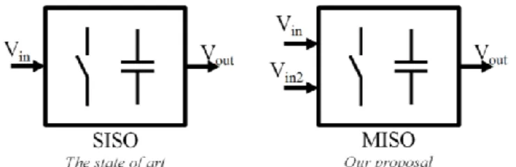
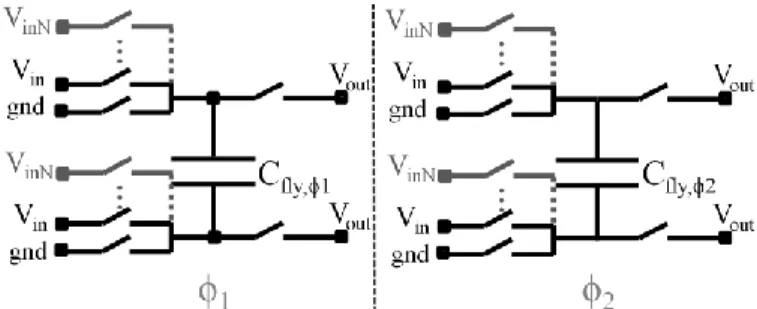
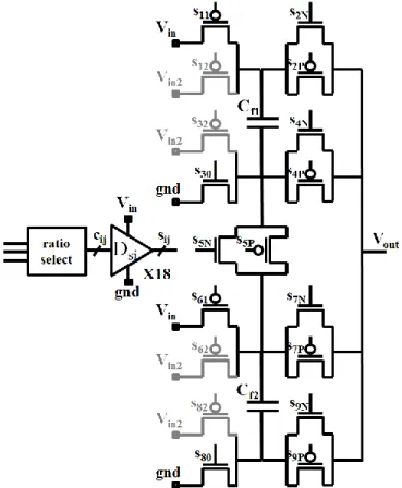
The versatile input interface is built on the same skeleton (see Fig. 2), but contrary to a conventional interface where every function is fixed, the

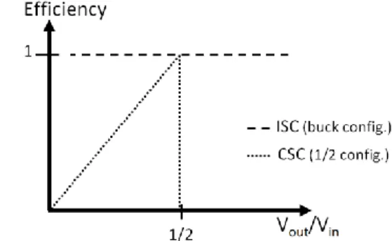
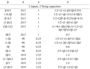
We here present a theoretical framework deriving the maximum efficiency achieved by a switched capacitor converter with respect to: the switching frequency, the capacitance value

Our formulae are Hobbs’s conjunctions of atomic predications, possibly involving FOL variables. Some of those variables will occur both in the LHS and the RHS of an I/O generator,

Significant power reduction can thus be achieved due to (i) the reduced sampling clock frequency by employing a fourth-order active-passive loop filter; (ii) the

Voltage to frequency conversion is a data acquisition technique widely used in synchrotron radiation and other scientific applications that require the proper

Pour ce faire, il faut donc qu’à chaque itération, les processus voisins se communiquent les états des cellules situées à leurs interfaces respectives.. Avec une

La fermentation acétique est un processus biochimique où l’éthanol est oxydé en acide acétique par le biais de bactéries acétiques dans des conditions stricts

Figure 5 provides a close-up view of the relation- ships between a component role (that model an abstract and partial view of a required component), a component type that models