HAL Id: hal-02524649
https://hal.archives-ouvertes.fr/hal-02524649
Submitted on 30 Mar 2020HAL is a multi-disciplinary open access archive for the deposit and dissemination of sci-entific research documents, whether they are pub-lished or not. The documents may come from teaching and research institutions in France or abroad, or from public or private research centers.
L’archive ouverte pluridisciplinaire HAL, est destinée au dépôt et à la diffusion de documents scientifiques de niveau recherche, publiés ou non, émanant des établissements d’enseignement et de recherche français ou étrangers, des laboratoires publics ou privés.
Evaluation of a Metal Supported Ni-YSZ / YSZ /
La2NiO4 IT-SOFC Elaborated by Physical Surface
Deposition Processes
Jérémie Fondard, Pierre Bertrand, Alain Billard, Stefan Skrabs, Thomas
Franco, Sébastien Fourcade, Pierre Batocchi, Fabrice Mauvy, Ghislaine
Bertrand, Pascal Briois
To cite this version:
Jérémie Fondard, Pierre Bertrand, Alain Billard, Stefan Skrabs, Thomas Franco, et al.. Evaluation of a Metal Supported Ni-YSZ / YSZ / La2NiO4 IT-SOFC Elaborated by Physical Surface Deposition Processes. ECS Transactions, 2015, 68 (1), pp.2303-2316. �10.1149/06801.2303ecst�. �hal-02524649�
OATAO is an open access repository that collects the work of Toulouse researchers and makes it freely available over the web where possible
This is an author's version published in: http://oatao.univ-toulouse.fr/25549
Official URL: https://doi.org/10.1149/06801.2303ecst
Any correspondence concerning this service should be sent
to the repository administrator: tech-oatao@listes-diff.inp-toulouse.fr
To cite this version:
Fondard, Jérémie and Bertrand, Pierre and Billard, Alain and Skrabs, Stefan and Franco, Thomas and Fourcade, Sébastien and Batocchi, Pierre and Mauvy, Fabrice and Bertrand, Ghislaine and Briois, Pascal Evaluation of a Metal Supported Ni-YSZ / Ni-YSZ / La2NiO4 IT-SOFC Elaborated by Physical Surface Deposition Processes. (2015) ECS Transactions, 68 (1). 2303-2316. ISSN 1938-6737
Evaluation of a Metal Supported Ni-YSZ / YSZ / La2NiO4 IT-SOFC
Elaborated by Physical Surface Deposition Processes
J. Fondarda,b, P. Bertranda, A. Billarda,b,c, S. Skrabsd, T. Francod, S. Fourcadee, P. Batocchie, F. Mauvye, G. Bertrandf , P. Brioisa,b
a
IRTES-LERMPS, UTBM, 90010 Belfort, France
b
FR FCLab 3539, 90000 Belfort, France
c
LRC CEA, UTBM, 90010 Belfort, France
d
PLANSEE SE, 6600 Reutte, Austria
e
ICMCB-CNRS, 87 Av. du Dr. A. Schweitzer 33608 Pessac Cedex, France
f
CIRIMAT UMR5085, ENSIACET, 4 allée E. Monso, 31030 Toulouse, France
The elaboration of the last generation metal supported IT-SOFC complete cell by dry surface deposition processes is really challenging. Atmospheric Plasma Spraying (APS) and Reactive Magnetron Sputtering (RMS) processes are respectively adapted to deposit Ni-YSZ anode and YSZ electrolyte layers. RMS is also used to coat a thin and dense La2NiO4 (LNO) cathode layer. In this
work, we have elaborated a complete cell on metallic support (ITM) produced by PLANSEE SE. The innovative LNO cathode layer was compared with screen-printed LNO layers, with and without RMS bonding layer. Electrochemical and Voltametry tests were performed on these samples. These revealed lower performances than literature due to the high density of the RMS cathode layer, and too high a temperature during sintering step which deteriorate layers manufactured by RMS and metallic substrate. Nevertheless, using LNO bonding layer manufactured by RMS seems to be an interesting way to improve the polarization resistance of the cell.
Introduction
Metal supported Intermediate-Temperature Solid Oxide Fuel Cell is employed to face with the reduction of SOFCs’ operating temperatures. The switch between anode supported cells and this new technology allows significant gains in term of cost, thanks to the mechanical support by a metal piece (1). Nevertheless, the use of a porous substrate presents some drawbacks. Thermomechanical and chemical compatibility problems between metallic and ceramic materials need to be solved. A diffusion barrier layer between metallic and ceramic materials permits avoiding the weakness of the substrate. A thin GDC layer, applied on the substrate before the anode layer, was identified as an appropriate solution (2). Moreover, the oxidation of the support could cause closing of its porosity, and deteriorate the performance of the cell (3). Therefore, it is necessary to use elaboration techniques of ceramics with no requirement of heat treatment at too high temperatures. Dry deposition techniques are a credible solution for the manufacturing of the core of the cell. Atmospheric Plasma Spraying process (APS) allows the realization of porous layers with very high deposition rate. This technique is also perfectly adapted for
10.1149/06801.2303ecst ©The Electrochemical Society ECS Transactions, 68 (1) 2303-2316 (2015)
the anode deposition on the porous substrate (4). Reactive Magnetron Sputtering (RMS) technique allows the deposition of thin and dense layers being able to be used as electrolyte (5) and diffusion barrier layers on the substrate / anode, and electrolyte / cathode (6) interfaces in fuel cells.
Whereas thick layers elaborated by wet deposition techniques are commonly used as cathodes in IT-SOFCs, recent studies deal with the deposition of Mixed Ionic and Electronic Conductors (MIECs) thin layers by physical surface deposition processes (7-8). RMS process may also deposit a cathode layer by the co-sputtering of several metallic targets (9). La2NiO4 is one of the most promising materials in IT-SOFCs. This K2NiF4
structured material presents interesting electrocatalytic properties (10), allowing its utilization as a thin cathode layer.
For this study, an ITM type porous metallic support manufactured by PLANSEE SE was employed for the cell assembling. This material presents very interesting thermal cycling resistance and durability properties keeping high electrochemical properties. Firstly, a GDC barrier layer was applied on the top of the substrate by RMS. A Ni-YSZ anode bi-layer material was secondly deposited by APS on metallic support. Then, a YSZ electrolyte material and a GDC barrier layer were applied by RMS after the polishing of the anode’s surface. The elaboration of this half-cell is partially described in a previous work (11). The most of the RMS coatings were deposited by the means of a Plasma Emission Monitoring (PEM) system, increasing the deposition rate of ceramics (12). LNO cathode layer was successively deposited by RMS. This step is detailed in a previous study (13).
In order to compare the efficiency of the experimental layer deposited by RMS as an individual cathode (RMS LNO) or a bonding cathode layer, the complete IT-SOFC building was elaborated by replacing and/or adding a screen-printed La2NiO4 material
(SP LNO). This layer was developed, optimized in ICMCB laboratory and allowed interesting performances on LNO/GDC/LNO half cells (14).
The overall cell performance comparison and detailed impedance analyses of the three different cells containing RMS LNO, SP LNO, and RMS LNO + SP LNO are presented to elucidate the difference between the complete cells.
Experiments
Reactive Magnetron Sputtering (RMS) Process
Two experimental devices were used for the different deposition processes. Systems are pumped down via a system combining XDS35i Dry Pump and a 5401CP turbo-molecular pump. Metallic targets were powered by a pinnacle + pulsed current generator from Advanced Energy. Tests were conducted in an argon and oxygen atmosphere. The flow rates were controlled with Brooks flowmeters and the pressure was measured using a MKS Baratron gauge.
A thin GDC layer was first applied on ITM metallic supports provided by PLANSEE SE. The experimental Alcatel604 device was used for this coating. The sputtering
chamber was equipped with four 50 mm diameter magnetron targets with a 250 mm rotating substrate holder parallel to the target at 120 mm. Samples were positioned at 55 mm from the axis of the substrate holder. Coatings were made in two steps by the co-sputtering of two Ce and Gd metallic targets with 120 sccm argon and 5 sccm oxygen flow rates.
The experimental device was a 100-litre Alcatel SCM 650 sputtering chamber pumped down for the other depositions after APS coating. The sputtering chamber was equipped with three 200 mm diameter magnetron targets and with a 620 mm diameter rotating substrate holder parallel to the targets at a distance of about 110 mm. The distance between the target axis and that of the substrate holder was 170 mm. Zr-Y (84-16% at), Ce-Gd (80-20% at), La and Ni metallic targets Substrates were positioned in front of the target at 170 mm from the axis of the rotating substrate holder in order to deposit homogenous coatings in terms of thickness and composition. The deposition stage was monitored using a closed loop control PEM (Plasma Emission Monitoring) system by optical emission spectroscopy (OES). The technique was based on the measurement of the optical intensity of the metal emission line in a volume near the target (12). The signal was sent via an optical fiber to a Ropper Scientific SpectraPro 500i spectrometer, with a 1200 groove mm−2 grating and a photomultiplier tube (Hamamatsu R 636). Subsequently, the information was transferred to a computer in which a program developed under Labview® controls the oxygen flow rate for keeping the optical intensity constant.
La2NiO4 coatings were deposited by co-sputtering two metallic targets. The PEM
system is employed on the target containing the main element of the coatings (La target). The intensity of the second target is adjusted in order to obtain the convenient compositions and structures. The as-deposited coating is amorphous. An annealing treatment at 1173 K for 2 h is necessary to crystallize it. Nevertheless, this treatment is too hard for the metallic substrate. Crystallization was performed at 1073 K during complete cell tests.
Atmospheric Plasma Spraying (APS) process
The plasma is generated in air at atmospheric pressure (APS) by a F4 plasma torch with a 6 mm internal nozzle diameter. A mixture of argon and hydrogen is used to form the plasma. The powder is injected by the means of carrier gas. It is introduced into the plasma via a 1.8 mm injector positioned at 6 mm from the exit of the outlet of the torch with a 90° angle. Samples are positioned on a fixed support at a distance of 90 mm from the plasma torch. The torch is controlled by a robot programmed to sweep samples surface with a step of 5 mm at a speed of 150 mm/s. Deposits were applied on ITM metallic substrate with GDC RMS layer. A 150 µm anode bi-layer was deposited from different powder sizes 59.5-40.5 wt% NiO-TSZ (YSZ with tetragonal phase) with different plasma spraying conditions in order to obtain high porosity with smooth surface condition. This elaboration is described in a previous work (15).
Screen-printing (SP) Process
The fine La2NiO4 powder was mixed into a solvent with a commercial dispersant
(21 mm diameter, 3.14 cm² by using a semi-automatic screen-printer Aurel MOD C890. A specific high-temperature sintering treatment was required in order to obtain a good adherence between the cathode layer of about 20 μm in thickness and the electrolyte/ or the bonding layer. The thermal cycle was as follows: an initial ramp at 1 K min−1
up to 673 K to eliminate organic binders, followed by a temperature increase up to the sintering temperature at 3 K min−1
. In order to avoid the deterioration of the metallic substrate, sintering step was performed at 1423 K under N2.
Characterization Devices
The morphology of the samples was characterized by Scanning Electron Microscopy (SEM) using a JEOL JSM 7800 F equipped with Energy Dispersive Spectroscopy (EDS) for chemical measurements. The structural features of the samples were performed in Bragg Brentano configuration X-ray diffraction using a BRUKER D8 focus diffractometer (CoKα1+α2 radiations) equipped with the LynxEye linear detector. XRD patterns were collected at room temperature during 10 min in the [20°-80°] scattering angle range by steps of 0.019°.
Single Cell Tests
The SOFC samples were inserted into a homemade set-up designed and built in the ICMCB laboratory. A nickel/gold grid was maintained on the cathode side with springs for current collection. Cathode layer was sintered for better crystallization at 1073 K during 10 h. Anode layer was reduced in situ step by step with H2/Ar mixtures at 973 K
during 6 h. Electrochemical measurements were performed at 973 K with 120 mL/min flow of H2 – 3 vol. % H2O on the anode side and 240 mL/min air flow on the cathode
side. The parameters for the Voltammetry measurements were 2 s equilibrium time, starting from OCV potential, to 0.2 V end potential with 5 mV/s scan speed. Electrochemical Impedance Spectroscopy (EIS) measurements were then collected at the Open Circuit Voltage (OCV) in the frequency range 100 mHz to 10 MHz with 10 points per decade.
Results
Figure 1 presents the reduction process of these different cells. This step was performed at 973 K from 6 to 120 mL/min of humidified H2 on the anode side. Increasing
oxygen flow rate leads to improve the OCV of the cells. The Open Circuit Voltage (OCV) of the cells with RMS LNO and SP LNO was measured at 0.9 V after cathode crystallization and anode reduction processes. This value is lower than the theoretical value of 1.05 V at this temperature and proves that the electrolyte tightness is not fully dense. With SP LNO coated on RMS bonding layer, OCV increase up to 0.95 V, pointing the efficiency of this additional layer. Differences between RMS samples and others are due to the previous cathode crystallization process of RMS cathode layer. This additional step (1073 K during 10 h) initiates the reduction process when the anodic side of the cell contains little hydrogen gas (95:5 vol % N2:H2). This results to higher initial OCV (0.21,
0.01 and 0.02 V for RMS, SP and RMS+SP samples respectively). The difference between samples with and without RMS bonding layer at each reduction step, underline
Figure 1. Evolution of complete cells’ open circuit voltage (OCV) during reduction of anode layer at 973 K.
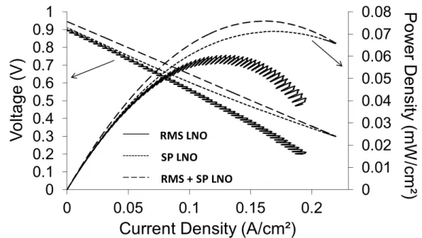
Figure 2 presents voltammetry tests of these complete cells. This measurement indicates a maximum power density of 60, 71 and 76 mW/cm². In the literature, metal-supported cells with anode and electrolyte manufactured by plasma spraying process and LSCF by screen-printing reach a power density of 500 mW/cm² at 1073 K (16). Cells presenting an electrolyte layer manufactured by reactive magnetron sputtering present a power density of 410 mW/cm² at 973 K (17) and the presence of really thin YSZ electrolyte with LSCF made by screen-printing can allow to reach much higher power densities (18). Some improvements of the cell microstructure and reduction of the thickness have to be performed in order to obtain better performances.
The electrochemical performances obtained with these different samples are in the same order of magnitude but SP LNO cathodes present higher power densities maybe due to higher active surface area. The RMS bonding layer allows an improvement too. This may increase the interface of the contacts layer between the electrode and the electrolyte.
According to the Ohm law, the total resistance of the cell can be determined by the slope calculation from the experimental I-E curve. In the low current density range, the ohmic resistance of the cell presenting RMS cathode is closed to 3.4 Ω.cm² and the resistance of the other cells is 3.1 Ω.cm². Nevertheless, as shown in the figure 2, at higher current density, the ohmic resistance of the SP LNO sample falls at 2.5 Ω.cm². This improvement might be induced by a switch between activation polarization and ohmic polarization. This observation confirms that the low performances observed could be due to electrode overpotentials.
its efficiency in this system. Indeed, OCV of sample presenting the bonding layer increases faster and the final value is higher (0.90 and 0.95 V for SP and RMS+SP respectively).
Figure 2. Voltametry tests of complete cells with RMS cathode, SP cathode and RMS + SP cathode layers.
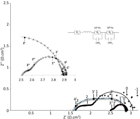
To explain these low performances, Electrochemical Impedance Spectroscopy (EIS) characterizations were also performed on these samples. Figure 3 presents typical Nyquist measurements of the complete cell under OCV. The Nyquist diagrams were fitted using Z-View software. Modeled data are represented by lines in the figures while experimental measurements are represented by data points. Four contributions characteristic of different phenomena appearing were identified in high, medium and low frequency ranges. Resistance and associated capacitance values were extracted from these fits.
Besides Nyquist diagrams were fitted by the same equivalent circuits, shapes of the impedance diagrams are fundamentally different, depending only on the cathode layer characteristics. Total resistances in the low frequency range are in the same order of magnitude, explaining performances measured on the different samples (figure 2). These different characteristics attributed for medium or low frequencies underline the different electrochemical phenomena occurrence on the different samples. The resistance at high frequencies remains same with “RMS” and “SP” samples but it is considerably higher with “RMS+SP” sample. The dense bonding cathode layer seems complicated to cross and induces two more interfaces. Nevertheless, this layer allows an interesting drop of the polarization resistance of the complete cell. In spite of its several interfaces and resistances, complete cell resistance remains the lowest. A decrease of the bonding layer’s thickness should considerably improve performances.
On the basis of the fitted data, the equivalent capacitance and the frequency relaxation of each contribution were calculated using relations (eq 1) and (eq 2).
��� = �� (1−�)
�
� ∗ �1 �� (�� 1)
with R: electrical resistance, n: decentering angle of the Constant Phase Element function, C: capacitance of the phenomenon.
Figure 3. Nyquist plots of complete cells with RMS cathode, SP cathode and RMS + SP cathode layers. Models are represented by lines. Experimental results are represented by points. Symbols represent the different samples: SP LNO (Х), RMS LNO (
◊
), RMS + SP LNO (○
).�� = 1 2�(���
���)1/�
� (�� 2)
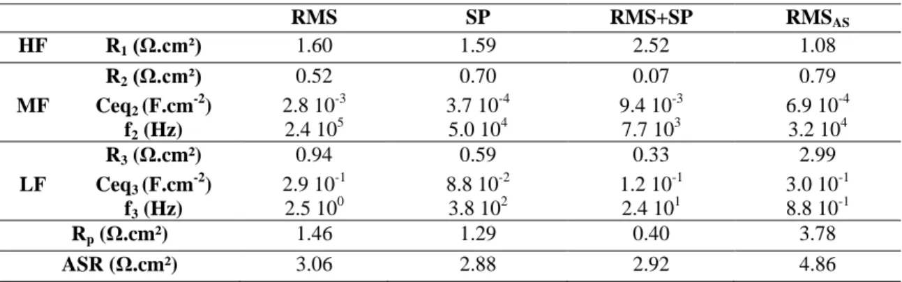
Table I presents the parameters of the different phenomena for each sample including a cell elaborated on commercial anode support with RMS cathode. High, Medium and Low frequency phenomenon are named by 1 (R1, Ceq1, f1), 2 (R2, Ceq2,f2) and 3 (R3,
Ceq3, f3) respectively. Polarization Resistance (Rp) is calculated by the sum of R2 and R3.
ASR represents the complete cell resistance.
Complete cells resistances ASR are much higher than requirements for IT-SOFCs (i.e. 0.8 Ω.cm²). These high values explain the poor performances obtained with these samples at 973 K. Numerous limitations could be induced by the use of several layers synthesized by different deposition techniques. The compatibility of these materials and structures has to be optimized in order to improve the performances by decreasing resistances.
According to the relaxation frequency and the equivalent capacitance values, three domains can be distinguished, at high frequency (HF), middle frequency (MF) and low frequency (LF), each representing a given electrochemical phenomenon. These results are presented in Table I.
Using the Schouler method (19), resistance and CPE have been assigned to specific electrochemical processes. According to literature on cathode half-cells with YSZ and GDC electrolyte, the low frequency range (LF) is characterized by high capacitance
3 2 3’ 1 2’ 0 3’’ 4’ -1 1’’0’ 2’’ 0.5 1 1.5 2 2.5 3 0.5 1 1.5 2 2.5 0 Z’ (Ω.cm2) Z ’’ ( Ω .cm 2)
TABLE I. Parameters determined by Electrochemical Impedance Spectroscopy RMS SP RMS+SP RMSAS HF R1(Ω.cm²) 1.60 1.59 2.52 1.08 R2(Ω.cm²) 0.52 0.70 0.07 0.79 MF Ceq2 (F.cm-2) f2 (Hz) 2.8 10-3 2.4 105 3.7 10-4 5.0 104 9.4 10-3 7.7 103 6.9 10-4 3.2 104 R3 (Ω.cm²) 0.94 0.59 0.33 2.99 LF Ceq3 (F.cm-2) f3 (Hz) 2.9 10-1 2.5 100 8.8 10-2 3.8 102 1.2 10-1 2.4 101 3.0 10-1 8.8 10-1 Rp (Ω.cm²) 1.46 1.29 0.40 3.78 ASR (Ω.cm²) 3.06 2.88 2.92 4.86
Because cathode material is the only variable parameter, and signal because, resistances and capacities are different, polarization resistance should be due to cathode material. Furthermore, single cell tests were performed on samples built from commercial anode support with RMS cathode in the same batch. LF phenomenon seems to be identical on the two samples (2.9×10⁻¹ F·cm-2 and 3.0×10⁻¹ F·cm-2 for RMS and RMSAS
respectively) confirming that this phenomenon could be due to the cathode. Nevertheless, equivalent capacitance and relaxation frequencies remain slightly different at MF. This phenomenon could be cathode and/or anode electrochemical phenomenon.
Values calculated are close to 10-3 F·cm-2 for the MF phenomenon and 1 F·cm-2 for the LF phenomenon (table I). Furthermore, resistance values of the MF phenomenon are significantly improved by the addition of the bonding layer (0.70 Ω.cm² and 0.07 Ω.cm² for SP and RMS+SP respectively). Bonding layer act as interface layer with the cathode material, this MF phenomenon could be assigned to ionic transfer at the electrode/electrolyte interface.
From these two last contributions at MF and HF, electrode polarization resistances of 0.4, 1.3, 1.5 Ω/cm² were determined for RMS+SP, SP and RMS respectively. Nevertheless, the specifications of fuel cell electrodes have to be lower than 0.5 Ω/cm². The high resistances obtained on RMS and SP samples are too high but probably not because of the same reasons. Analyses of structures and microstructures of electrolyte, cathode and interface have to be checked to pointed out differences between samples and explain results.
Figure 4 presents structure comparison of the cathode materials after tests. Due to a thinner cathode layer on the RMS sample, GDC substrate’s structure is identified. XRD measurements of SP and RMS+SP samples remain the same because the cathode layer is too thick to see the bonding layer. Unidentified peak is related to the satellite peak of the (113) peak, appearing at lower angle.
values, Ceq ≈ 1−10 F· cm -2
(14, 20). This contribution was assigned to the gaseous diffusion through the electrode. The capacitance of the medium frequency contribution (MF) is found to be higher, Ceq ≈ 10
-3
–10-1 F·cm-2. The source of this impedance contribution is more complicated to identify, it has been assigned as Oxygen Reduction Reaction (ORR) itself occurring at the electrode/gas interface in literature (14, 21) and/or ionic transfers at the electrode/electrolyte interface (22).
Figure 4. XRD measurements of RMS, SP and RMS+SP complete cells.
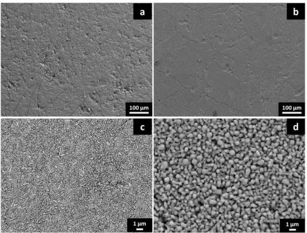
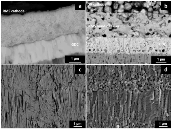
Figure 5 shows SEM observations of surface microstructure of the different samples after tests. Surface condition of every sample is not completely smooth and presents strains due to the surface condition of the metallic substrate and the APS anode (figure 5 a, c). But this should not involve electrochemical problems. With higher magnification, microstructure of cathode coatings is totally different, as expected. While RMS coating is fully dense, SP coating present high content of porosities.
SEM observations of samples cross sections are presented figure 6 and 7. Samples presenting LNO cathode manufactured by screen-printing process need high temperature sintering treatment to optimize the adherence of the layer. Nevertheless, this annealing treatment (1423 K for 12 h under nitrogen atmosphere) induces microstructural changes. While sample with RMS LNO layer presents dense layers (figure 6a and figure 7a, c), sintered samples present more porosities (figure 6b, c and figure 7b, d). Indeed, small sized porosities appear in all RMS layers and at interfaces. Images analyses have been performed by Image J software on SEM micrographs. It reveal 10 ± 2 % porosity with 0.006 ± 0.004 µm² surface (≈ 90 nm average porosity diameter if considered as perfect sphere) inside electrolyte layer on RMS+SP sample, and 16 ± 3 % porosity with 0.024 ± 0.009 µm² surface (≈ 180 nm average porosity diameter). Nevertheless, this analysis could not be done on RMS sample. This increase of porosity is well-known on coatings deposited with EB-PVD process with columnar microstructure at high temperature. Space between thin and thick column increase during high temperature annealing and spherical porosity appears along the thicker column (23).
The same tetragonal lanthanum nickelate phase was identified without major impurities. A slight preferential orientation difference could be noted between cathode deposited by RMS and SP. It should have no effect on cathode characteristics.
Figure 5. Surface microstructure of samples with RMS (a,c) and SP cathodes (b,d) with different magnifications.
Figure 7. Cross section of samples with RMS (a,c), and RMS+SP (b,d) samples. Zoom on RMS nickelate lanthanum layer (a,b). Zoom on electrolyte material (c,d).
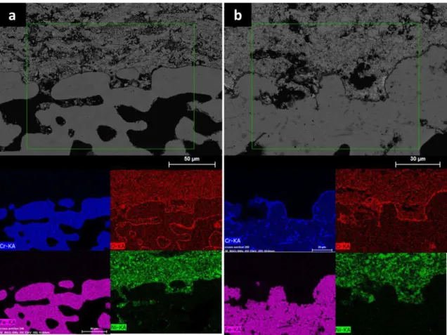
Figure 8 shows the EDS mapping of the porous metallic support on the different samples after tests. Each sample present a thin Cr2O3 oxidation protective layer but it is
thicker with SP sample, due to higher time and temperature annealing, even in very low oxygen partial pressure condition (nitrogen gas). Results found in literature prove the formation of chromia layer on metallic support in these conditions, but no evidence of deterioration was pointed in these works (3, 18). Nevertheless, chromia layer should act The porosity appearing in electrolyte (figure 7d) is not open because the OCV of the cell remains same on RMS and SP samples (i.e. 0.9 V) as seen in figure 2.
RMS LNO layer does not present columnar structure as shown in figure 7a. Analyses were performed in another work on LNO and PNO cathode, this increase of porosity was also identified since 1323 K. EDS measurements were performed on the surface of these samples, and showed a decrease of La and Pr content in LNO and PNO materials, which may change structural and compositional characteristics of this layer. This fact could involve different electrochemical performances between RMS cathode and RMS bonding layer. EDS profiles and mappings, performed on polished cross section of samples, confirms a slightly lack of lanthanum but not significant. No element diffusion was detected between electrolyte and cathodes, showing the chemical stability of these layers. The increase of porosity, induced by the sintering treatment of the SP LNO cathode, may improve electrochemical behavior of the bonding layer but it provokes porosity inside the electrolyte and interfaces with GDC layers which slow the ionic diffusion. These phenomena could increase resistances and explain poor performances of the cells.
Figure 8. EDS mapping of the porous metallic support after complete cell tests with RMS (a) and SP (b) samples. SP sample was annealed at 1423 K during 12 h.
Conclusion
A GDC/Ni-YSZ/YSZ/GDC/La2NiO4 complete cell was elaborated on porous metallic
substrate by physical surface deposition processes and successfully tested at 973 K in air and hydrogen atmosphere. Deposition of dense RMS LNO coating was very challenging as electronic diffusion barrier and could impact performances. Further experiments have to be performed to check it.
No nickel and/or chromium interdiffusion between support and anode layer was evidenced proving the positive effect of GDC protective diffusion layer reported in some studies (2), as shown in figure 8 a, b. Moreover, no nickel agglomeration was underlined in anode layer, detected in some publications with long term annealing treatment (24). However, figure 8b underlines microstructural modifications in the metallic substrate. Cr element diffuses easily to the interface and some areas are lack of Cr. These Cr-rich areas seem to be lack of Fe element.
These compositional and microstructural modifications of the substrate could explain poor performances of the cells. Complete cell tests have to be performed on these samples elaborated on commercial anode support to check the influence of the support deterioration on performances.
1. M.C. Tucker, Journal of Power Sources, 195, 4570-4582 (2010).
2. P. Blennow, J. Hjelm, T. Klemenso, S. Ramousse, A. Kromp, A. Leonide, A. Weber, Journal of Power Sources, 196, 7117-7125 (2011).
3. M. Brandner, M. Bram, J. Froitzheim, H.P. Buchkremer, D. Stöver, Solid State
Ionics, 179, 1501-1504 (2008).
4. R. Vaβen, D. Hatiramani, J. Mertens, V.A.C. Haanappel, I.C. Vinke, Surface and
Coatings Technology, 202, 499-508 (2007).
5. P. Briois, A. Billard, Surface and Coatings Technology, 201, 1328-1334 (2006). as metal-supported IT-SOFC’s cathode material or bonding layer with porous cathode layer. Different samples were manufactured with RMS LNO, SP LNO and SP LNO with RMS LNO bonding layer in order to test different configurations and compare results. Open Circuit Voltage measurements of these cells are promising, revealing 0.9 V for RMS and SP cells, and reaching 0.95 V for RMS+SP cell presenting more layer than the others. However, tests of these cells reveal poor performances for each cell (60, 71 and 76 mW/cm² for RMS, SP and RMS+SP respectively). Impedance Spectroscopy of these cells reveals high resistances. Limitations can be due to each component of the cell, because of high serial resistance (electrolyte, support) and high polarization resistance of RMS and SP cells. In spite of numerous advantages, the use of metal substrate induces some constrains. Its higher temperature resistance especially under oxidizing atmosphere is the most important one. Nevertheless, layers deposited by screen-printing process need sintering process performed at high temperature during long time to improve their adherence. While the crystallization treatment (1073 K during 10 h) does not change microstructure of the cell and substrate, the sintering treatment creates porosity in electrolyte, interfaces and deteriorates the metallic substrate. These conditions explain poor performances of the cells presenting screen-printed cathodes. Bad performances of the RMS cell are mainly due to the high density of the cathode, lowering oxygen reduction and ionic diffusion processes. Each layer proved their efficiency because no interdiffusion was detected in support/anode and electrolyte/cathode interfaces even after sintering process. Optimization of electrolyte microstructure and layers thicknesses has to be performed in order to improve performances. Additional studies have to be done, to find a way to avoid the substrate deterioration during sintering process and complete cell tests. In spite of poor performances of RMS cathode layer, RMS LNO bonding layer show really promising results. Indeed, it allows significantly lowering the polarization resistance and improving OCV of the cell. The major improvement of this bonding layer is to increase ionic transfer at electrolyte/cathode interface. The thickness of this layer has to be optimized to lower serial resistance while maintaining OCV.
Acknowledgments
This study was granted by the Pays de Montbéliard Agglomeration. Authors acknowledge Plansee for their contribution of the porous metal support employed in this study.
6. N. Jordan, W. Assenmacher, S. Uhlenbruck, V.A.C. Haanappel, H.P. Buchkremer, D. Stöver, W. Mader, Solid State Ionics, 179, 919-923 (2008).
7. I. Garbayo, V; Esposito, S. Sanna, A. Morata, D. Pla, L. Fonseca, N. Sabaté, A. Taracon, Journal of Power Sources, 248, 1042-1049 (2014).
8. H-S Noh, K.J Yoon, B-K Kim, H-J Je, H-W Lee, J-H Lee, J-W Son, Journal of
Power Sources, 247, 105-111 (2014).
9. P. Briois, F. Perry, A. Billard, Thin Solid Films, 516, 3282-3286 (2008).
10. E. Boehm, J.-M. Bassat, P. Dordor, F. Mauvy, J-C.Grenier, Ph. Stevens, Solid
State Ionics, 176, 2717 – 2725 (2005).
11. J. Fondard, P. Bertrand, A. Billard, S. Skrabs, Th. Franco, G. Bertrand, P. Briois,
Electrochemical Society Transactions, 57, 673-682 (2013).
12. F. Perry, A. Billard, C. Frantz, Surface Coatings Technology, 94-95, 681-685 (1997).
13. J. Fondard, A. Billard, G. Bertrand, P. Briois, Solid State Ionics, 265, 73-79 (2014).
14. B. Philippeau, F. Mauvy, C. Mazataud, S. Fourcade, J-C. Grenier, Solid State
Ionics, 249-250, 17-25 (2013).
15. J. Fondard, P. Bertrand, A. Billard, G. Bertrand, S. Skrabs, Th. Franco, P. Briois,
Transportation Electrification Asia-Pacific (ITEC AsiaPacific) 2014 IEEE conference expo, DOI: 10.1109/ITEC-AP.2014.6941042 (2014).
16.D. Hatiramani, R. Vaβen, D. Stöver, R.J. Damani, Journal of Thermal Spray
Technology, 15, 593-597 (2006).
17. H. Wang, W. Ji, L. Zhang, Y. Gong, B. Xie, Y. Jiang, Y. Song, Solid State Ionics, 192, 413-418 (2011).
18. R. Nédélec, S. Uhlenbruck, D. Sebold, V.A.C. Haanappel, H.P. Buchkremer, D. Stöver, Journal of Power Sources, 205, 157-163 (2012).
19. E.J.L. Schouler, M; Kleitz, Journal of Electrochemical Society, 134, 1045-1050 (1987).
20. L. Mogni, N. Grunbaum, F. Prado, A. Caneiro, Journal of Electrochemical
Society, 158, B202-B207 (2011).
21.M.J. Escudero, A. Aguadero, J.A. Alonso, L. Daza, Journal of Electroanalytical
Chemistry, 611, 107-116 (2007).
22.J. Dailly, S. Fourcade, A. Largeteau, F. Mauvy, J.C. Grenier, M. Marrony,
Electrochimica Acta, 55, 5847–5853 (2010).
23. X. Zhao, X. Wang, P. Xiao, Surface and Coatings Technology, 200, 5946–5955 (2006).