HAL Id: tel-02434306
https://tel.archives-ouvertes.fr/tel-02434306v2
Submitted on 5 Mar 2020
HAL is a multi-disciplinary open access archive for the deposit and dissemination of sci-entific research documents, whether they are pub-lished or not. The documents may come from teaching and research institutions in France or abroad, or from public or private research centers.
L’archive ouverte pluridisciplinaire HAL, est destinée au dépôt et à la diffusion de documents scientifiques de niveau recherche, publiés ou non, émanant des établissements d’enseignement et de recherche français ou étrangers, des laboratoires publics ou privés.
Investigation of Al thermal diffusion in SixGe1-x alloy
nanowires using in-situ transmission electron microscopy
Minh Anh Luong
To cite this version:
Minh Anh Luong. Investigation of Al thermal diffusion in SixGe1-x alloy nanowires using in-situ transmission electron microscopy. Materials Science [cond-mat.mtrl-sci]. Université Grenoble Alpes, 2019. English. �NNT : 2019GREAY050�. �tel-02434306v2�
THÈSE
Pour obtenir le grade de
DOCTEUR DE LA
COMMUNAUTÉ UNIVERSITÉ GRENOBLE ALPES
Spécialité : NANOPHYSIQUE Arrêté ministériel : 25 mai 2016
Présentée par
Minh Anh LUONG
Thèse dirigée par Eric ROBIN et Martien den HERTOG
préparée au sein du CEA/IRIG/DEPHY/MEM/LEMMA et Institut
Neel CNRS
dans l'École Doctorale Physique
Etude de la diffusion thermique de l'Aluminium
dans des nanofils de Germanium et en alliages de Si
xGe
1-xen utilisant la microscopie électronique en transmission
in situ
Investigation of Al thermal diffusion in Ge and Si
xGe
1-xalloy nanowires using in-situ transmission electron
microscopy
Thèse soutenue publiquement le 5 Novembre 2019, devant le jury composé de :
M. Gilles PATRIARCHE
Directeur de Recherche CNRS ÎIe-de-France Gif-sur-Yvette, Rapporteur M. Dinh Phong TRAN
Professeur Assistant USTH – Vietnam, Rapporteur Mme Catherine BOUGEROL
Directrice de Recherche CNRS Delegation Alpes, Président M. Alois LUGSTEIN
ii To my parents,
iii
Acknowledgements
Before going through all the stressful, but passionated scientific works, I would like to express my gratitude to all the people who have been consistently supporting me out throughout three years of my PhD. First and foremost, I would like to specially thank my two amazing supervisors, Dr. Martien den Hertog and Dr. Eric Robin for your expertise and continuous support. Dr. Martien, discussing with you always bring me lots of motivation and encouragement. Your pedagogical way of teaching and limitless patience helps me a lot in tackling problems and inspiring me in learning new subjects. Dr. Eric, thank you for spending your valuable time teaching me how to use the microscopes, for all the knowledge and your daily support. On a more personal note, my wife and I appreciate very much your lovely gifts for our marriage.
Besides, I would like to send my sincere respect to all the members in CEA/IRIG-DEPHY/MEM/LEMMA lab: Dr. Nicolas, Laure, Jean-Luc and Hanako for your technical helps and giving me a friendly working atmosphere. Sincere thanks to all my colleagues in CEA Minatec: Carlos, Dipankar, Andrea, Ahmed, Praveen and Zahra for daily funny jokes and constructive conversations in research experiences. Without you guys, I could never have many wonderful memories in Grenoble city. Additionally, I would like to thank LANEF funding, for give me a chance to come to France, immerse in a professional scientific work and start my future.
Finally, I would like to thank my family, my wife and all my lovely non-physicist friends for always sticking up with me, giving me daily inspiration and energy to finish this work.
v
Abbreviations and Symbols List of Abbreviations
Abbreviation Full Meaning
NWs Nanowires
1D One Dimensional
ALD Atomic Layer Deposition
CVD Chemical Vapour Deposition
VLS Vapor–Liquid–Solid
VSS Vapor–Solid- Solid
TA Template-Assisted
EBL Electron Beam Lithography
QCM Quartz Crystal Microbalance
CMOS Complementary Metal Oxide Semiconductor
FETs Field Effect Transistors
LEDs Light-Emitting Diodes
HF Hydroflouric Acid
HI Hydroiodic Acid
PMMA Poly(methyl methacrylate)
MIBK Methyl Isobutyl Ketone
IPO Isopropanol
BOE Buffered Oxide Etch
DIW Deionized Water
Al2O3 Aluminium oxide
Si3N4 Silicon nitride
LaB6 Lanthanum hexaboride
W Tungsten
TMA Al(CH3)3 [Trimethylaluminum]
TEM Transmission Electron Microscopy
STEM Scanning Transmission Electron Microscopy
HAADF High-Angle Annular Dark-Field
HRTEM High Resolution Transmission Electron Microscopy
FT Fourier Transformation
DP Diffraction Pattern
SEM Scanning Electron Microscope
vi
List of Symbols
Symbol Full Meaning
Å Angstrom
eV Electron Volt
nm Nanometer
s Second
Eg Bandgap Energy
EELS Electron Energy Loss Spectroscopy
RTA Rapid Thermal Annealing
SDD Silicon Drift Detectors
TMP Turbo Molecular Pump
RP Rotary Pump
QCM Quartz Crystal Microbalance
TLM Transfer Length Measurement
CB Conduction Band
Table of Contents
Acknowledgements ... iii
Abbreviations and Symbols ... v
Chapter 1: Introduction 1.1 Historical Context of Semiconductor Devices ... 5
1.2 Objective of this PhD Thesis ... 6
1.3 Thesis Outline ... 9
1.4 Author Contributions ... 10
Chapter 2: Introduction to Silicide and Germanide Phases 2.1 Background ... 11
2.2 Kinetics of Thermal Exchange Reaction ... 13
2.3 Band Alignment of Metal/Semiconductor Junction ... 15
Chapter 3: Sample Fabrication 3.1 Potential of Nanowires ... 21
3.2 Semiconductor Nanowire Growth ... 22
3.3 NWs Preparation ... 24
3.3.1 Detection of Highly n-doped Shell ... 24
3.3.2 Hydro Peroxide (H2O2) Etching of n-doped Ge Shell ... 25
3.3.3 HI Acid Etching of GeO2 Shell ... 26
3.3.4 Atomic Layer Deposition (ALD) ... 27
3.4 Ebeam Lithography ... 29
3.4.1 NWs Dispersion ... 29
3.4.2 Spin Coating of Resist ... 31
3.4.3 Exposure of Resist ... 32
3.4.4 Development ... 32
3.5 Buffered Oxide Etching (BOE) ... 33
3.6 Al Deposition ... 34
3.6.1 Ar Plasma Cleaning ... 34
3.6.2 Al Deposition by Sputtering and Electron Beam Evaporation ... 35
3.7 Lift Off ... 37
3.8 Rapid Thermal Annealing (RTA) ... 37
2
3.10 Conclusion ... 40
Chapter 4: Electron Microscopy Techniques 4.1 Introduction ... 42
4.2 Scanning Electron Microscopy (SEM) ... 44
4.3 Transmission Electron Microscopy (TEM) ... 47
4.3.1 Components ... 48
4.3.1.1 Electron Gun ... 49
4.3.1.2 Electromagnetic Lens and Apertures ... 50
4.3.1.3 Deflection Coils ... 52
4.3.1.4 TEM Holder and Compustage ... 53
4.3.1.5 Diffraction Lens and Projection System ... 54
4.3.1.6 Fluorescence Screen and CCD Cameras ... 55
4.3.1.7 Vacuum System and Cold Trap ... 55
4.3.2 TEM-STEM Mode ... 55
4.3.2.1 TEM Mode ... 56
4.3.2.2 STEM Mode ... 58
4.4 In-situ (S)TEM Heating Techniques ... 60
4.4.1 Direct Joule Heating Method ... 60
4.4.2 Temperature Calibrated Heater Chip ... 63
4.5 Geometrical Phase Analysis (GPA) ... 64
4.6 Quantitative EDX: Compositional Analysis of Created Heterostructures ... 65
4.6.1 Background ... 66
4.6.2 Quantitative Analysis ... 68
4.6.2.1 K- ratio Method by Raimond Castaing. ... 68
4.6.2.2 Cliff and Lorimer Ratio Method ... 70
4.6.2.3 Zeta Factor Method ... 71
4.6.3 3D Reconstruction ... 73
Chapter 5: Solid-State Reaction of Al/Ge Binary System 5.1 Background ... 77
5.2 Experimental ... 79
5.3 The Nucleation of the Exchange Reaction and Degradation of the Al Heater ... 81
5.4 Effect of Electron Beam on the Reaction Interface Propagation Rate ... 85
5.5 Influence of NW Diameter on Propagation Rate... 86
5.6 Radial and Axial Propagation of the Al/Ge Interface – Effect of Al2O3 Shell ... 88
3
5.8 The influence of Al Sputtering/E-beam Evaporation on the Solid-State Reaction ... 93
5.9 Combining Ex-Situ and In-Situ Heating to Produce an Ultra-Small Ge QD ... 94
5.10 Electrical Measurements on Short Ge NW Segments ... 97
5.10.1 Maximum Electrical Conduction of Short Ge Segments... 97
5.10.2 Measurements of Contact Resistance in Doped Ge NWs ... 99
5.10.2.1 Al/Ge Contact Quality before the Thermal Exchange Reaction ... 100
5.10.2.2 Al/Ge Contact Quality after the Thermal Exchange Reaction ... 100
5.11 Dopant “Pile-up” in Ge NWs ... 101
5.11.1 Detection of the n-doped Shell around the Ge NWs ... 102
5.11.2 Removing of n-doped Shell for Phosphorous Concentration Measurement ... 105
5.12 Conclusion ... 106
Chapter 6: Solid-State Reaction of Al- (Si, Ge) Ternary System 6.1 Background ... 108
6.2 Experimental ... 111
6.3 In-situ Heating Experiment: Real Time Observation of Thermal Exchange Reaction ... 112
6.3.1 During the Heating Process: Formation of a Double Interface Region ... 112
6.3.2 During the Cooling Process ... 114
6.4 Ex-Situ Heating Experiment: The Formation of Al/Si/Si0.67Ge0.33 Heterostructures ... 116
6.5 Quantitative EDX: Compositional Analysis of Al/Si/Si0.67Ge0.33 Heterostructures ... 118
6.6 Influence of NW Diameter on the Diffusion Rate ... 120
6.7 Influence of the Cooling Speed on the Si-rich Segment Length ... 121
6.8 Influence of Al2O3 Shell on the Si0.67Ge0.33 Interface Shape ... 123
6.9 Thermal Exchange Reaction in Large NW Diameters (≥ 150 nm) ... 125
6.9.1 During the Heating Process ... 125
6.9.2 During the Cooling Process ... 127
6.10 Mechanism of the Exchange Reaction in Small NW Diameters (≤ 100 nm) ... 128
6.11 Mechanism of the Exchange Reaction in Passivated NWs ... 130
6.12 The Electrical Transport Characteristics of Al/Si/Si0.67Ge0.33 Heterostructures ... 131
6.13 Conclusion ... 132
Chapter 7: Conclusions and Perspectives 7.1 Conclusions ... 133
7.1.1 On the thermally activated solid-state reaction in the Al/Ge binary system ... 133
7.1.2 On the thermally activated solid-state reaction in the Al- (Si, Ge) ternary system .... 134
7.2 Perspectives ... 136
4
7.2.2 For Al- (Si, Ge) NW Ternary ... 137
7.2.3 Thermal Exchange Reaction in Core-Shell NW Systems ... 137
Appendix A A1. Al Thermal Diffusion in Ge - Si Core - Shell NWs... 139
A1.1. Experimental ... 139
A1.2. Structural and Compositional Analysis ... 139
A2. Al Thermal Diffusion in Si – Ge Core - Shell NWs ... 143
A2.1. Experimental ... 142
A2.2. Structural and Compositional Analysis ... 143
Supporting Information ... 147
References ... 148
5
Chapter 1
Introduction
This PhD is about transmission electron microscopy using in-situ observation of a thermally induced reaction between a metal and a semiconducting nanowire. Before going to the objectives of the PhD thesis, we would like to present a brief history of microelectronic development with respect to the mainstream of Si(Ge)- based nanotechnologies and the reasons behind this work.
1.1 Historical Context of Semiconductor Devices
In 1926, Julius Edgar Lilienfeld first patterned a three-electrode structure using copper-sulfide semiconductor material [1], which is nowadays considered as a field-effect transistor, the fundamental building block of electronic devices. About 28 years later, in 1954, the first full transistorized computer named “The TRADIC (TRAnsistor DIgital Computer or TRansistorized Airborne DIgital Computer) was made in Bell Labs (USA) lead by Jean Howard Felker [2]. At that time, the machine was a mere three cubic feet and contained almost 800 point-contact transistors and 10,000 germanium crystal rectifiers. Since then, the world has witnessed a rapid technological innovation, especially with the replacement of germanium by silicon due to its abundant resources, novel mechanical-electrical properties and stable SiO2. Due to the continuous technological
developments, the size of electrical components is shrinking down to nanoscales, giving a tremendous density of electrical components in an integrated circuit. Stated in the paper published in 1957, Gordon Moore predicted that the number of the transistors in an integrated circuit would double every two years [3]. This statement remains more or less valid until today as chip manufacturers (e.g. Intel and Samsung) continue shrinking the transistor’s size with the 10- and 7 nm nodes [4,5]. Nowadays, high-tech devices are exponentially introduced, and are present in most of the aspects of our life. It is a matter of fact that people are familiar with the technological term “nanotechnologies” rather than “micro-technologies”. According to the announcement of Apple company in 2018 [6], they have introduced the A12X octa-core processor with the 7 nm technology and the ability to compact 10 billion transistors per 122 mm2 unit area. Other companies are also joining the aggressive race of producing the most powerful processing chips in recent years.
6 On the other hand, the miniaturization of conventional MOSFET structures is coming to a halt due to several challenges such as the leakage current through the gate oxide layer and limited doping control: in short channel transistors statistical variations in doping can lead to large variability and degradation of on/off switching characteristics [7]. Due to the integration of a high density of electrical components on a limited chip area, the temperature rise causes problems of the power consumption and operation efficiency. At the annual American Physical Society meeting at Caltech on December 29, 1959 [8], Richard Feynman had given a famous speech: “There's
Plenty of Room at the Bottom”. This sentence might be no more valid for the next ten years.
Therefore, besides trying to shrink down the electrical components, people are also looking for new materials and architectures to satisfy the growing demands of fast performance and higher efficiency. Germanium returns to interest due to its excellent carrier mobility (having the highest hole mobility among semiconductors and the electron mobility is 2.5 times larger than in silicon) and the compatibility with the existing Si platform. Furthermore, for optical applications, the indirect bandgap of Ge (Eg = 0.66 eV) is just 140 meV below its direct band gap (0.80 eV).
Therefore, it is possible to transform its indirect bandgap to direct bandgap by tensile strains (1.8 - 1.9%) or doping (7×1019 cm-3) [9,10]. SixGey alloy is also attracting attention as its bandgap energy
can be tailored with the compound stoichiometry, which can bring promising applications for near-infrared (NIR) detection [11]. Compared with the conventional planar bulk MOSFET channel, new architectures such as nanowires (NWs), carbon nanotubes (CNTs), nanoparticles (NPs) or quantum dots (QDs) are getting more interests due to their confinement effects.
1.2 Objective of this PhD Thesis
Since the last decade, the protruding of metals in semiconductor NWs has become a well-known process to reduce the contact resistance at the metal/semiconductor interface. The advantage of this approach is that upon heating the metal enters the semiconducting NW at both ends, creating intermetallic regions in the NW. If the process is well controlled and stopped at the right moment, only a thin section of semiconductor is left between metallic contacts, allowing to fabricate electrically contacted quantum-dot in a wire structures in a single fabrication step. The Al/Ge system in NWs appears very promising since, in contrast to other metal-semiconductor combinations, no intermetallic phase is formed and a pure monocrystalline Al NW is created with a very sharp interface with the remaining Ge NW. Moreover, the combination of the intrinsically
7 strong spin−orbit coupling in Ge and the superconducting properties of Al make this system a promising platform to study hybrid superconductor-semiconductor devices [12]. Previously, the diffusion behavior and kinetics of the thermal exchange reaction of the Al/Ge binary system have been carefully studied by El Hajraoui [13]. However, the real-time observation of the exchange reaction at the nucleation stage and the control of the growth rate at an atomic scale is still under-investigated. In addition, when studying the diffusion behavior of the Al/Ge reaction interface, he incidentally observed the presence of a thin Si layer between the reacted and unreacted part. Since the investigated NWs are pure Ge NWs, the presence of Si is attributed to contamination. It would be interesting to protrude Al metal in SixGe1-x alloy NWs, expecting to produce Al/Si/SixGe1-x
nanowire heterostructures, which have shown a great potential for near infrared (NIR) or mid-wave infrared (MWIR) photodetectors [11,14].
To these above interests, the PhD thesis is set up with two targets: (i) to study the thermally induced solid state reaction of the Al/Ge binary system with the aim to deterministically fabricate Ge QDs with atomic size control between perfectly sharp metal contacts, (ii) to exploit the thermal reaction of Al metal in SixGe1-x alloy NWs, which has not been reported in literature. To these
goals, ex-situ and in-situ heating experiments are carried out for observing the formation and real time propagation of the reaction interface.
(i) For the Al/Ge binary material combination, it has been reported in the work of El Hajraoui [13] that the intrusion of Al in Ge NWs will result in the formation of a monocrystalline Al core with face-centered cubic (FCC) structure. The pure Al core is surrounded by a thin pure Ge (∼2 nm), Al2O3 (∼3 nm), and Ge containing Al2O3 (~1 nm) layer, respectively. Combining kinetic
studies of the reaction interface with three dimensional chemical modelling, he proposes a surface diffusion mechanism in the Al/Ge binary nanowire system where Ge atoms diffuse through a surface diffusion channel on the created Al NW into the Al contact pad, while Al atoms are supplied to the reaction interface by Al self-diffusion and exchange with Ge atoms at the interface. The electrical and optical transport properties of Al/Ge/Al heterostructures were elucidated in the work of Sistani et al [15] and Staudinger et al [16], where they showed quantum ballistic transport as well as quantum ballistic photo-detection at room temperature. Following these results, in our work, in-situ TEM Joule heating experiments are conducted to follow the reaction interface from the initial stage of nucleation underneath the metal/nanowire contact pad to the end of the exchange
8 process. Then, we investigate different parameters that can affect the diffusion rate, aiming to control the diffusion process with atomic scale precision and produce ultra-small Ge segments. The in-situ heating experiments are performed using home fabricated Si3N4 membrane chips flowing a
current through a metal strip defined on the NW by electron beam lithography, that will heat up due to Joule heating. The electrical transport properties through the small Ge segments will also be investigated. Finally, we verify if the thermally-induced propagation of the metal phase along the NW may lead to the modification of the doping concentration next to the contact due to the so-called “doping pile-up”, i.e. the dopant atoms are not integrated in the metallic phase but pushed forward into the semiconducting region [17].
(ii) For the Al-(Si, Ge) ternary system, there are a number of studies on the thermal diffusion of Al-Si, Al-Ge and Al-(Si, Ge) in bulk and thin film materials [18–20]. However, in a 1D system, the understanding of the thermal reaction is still limited. While Al can easily diffuse into Ge NWs at low temperature (< 300 oC), there is no report of Al thermal diffusion in Si NWs. This is mainly
due to the low solubility of Si in Al and vice versa [21]. Therefore, to initiate the exchange reaction in SixGe1-x alloy NWs, it is expected that higher temperatures are needed than in Ge NWs, that
can’t be reached using direct Joule heating. Therefore, ex-situ heating via rapid thermal annealing (RTA) and in-situ TEM heating using commercial chips (from DENSsolutions company [22]) will be used to study the Al-(Si, Ge) ternary system in a NW. The structure and composition of the generated heterostructures will be studied via geometrical phase analysis (GPA) and quantitative EDX for an understanding of the diffusion behavior and kinetics. Different factors such as NW diameter, surface quality and annealing conditions are also investigated for the interpretation of the diffusion mechanism. Finally, the transport measurement on the propagated NWs will be conducted to evaluate the potential for device applications.
9
1.3 Thesis Outline
In chapter 2, we present a literature review of the thermally activated solid-state reaction of metals in Si/Ge semiconductor nanowires with a highlight on the diffusion mechanisms. Some typical examples for state of the art nanowire applications are also demonstrated, showing a promising future for metal-silicide (germanide) for applications in modern technology. Then, the basic theory of bandgap alignments in a metal/semiconductor junction is described, which is useful for understanding the electrical transport property of electronic devices.
In the chapter 3, we present the detailed protocol of the sample fabrication process, including the interest of low dimensional nanowire materials, NW growth, processes of NW contacting via electron beam lithography and basic principle of ex-situ heating via the rapid thermal annealing technique (RTA).
In chapter 4, basic principles of electron microscopy techniques (SEM and TEM) used in this study and their subsequent applications for the structure and composition analyses such as GPA and quantitative EDX (with the 3D reconstruction) are presented. Finally, we explain the principle and electrical set-up for in-situ Joule heating experiments.
In the chapter 5, we present results on the thermally assisted solid state exchange reaction in the Al/Ge binary NW system. The thermal diffusion behaviors in the Al/Ge binary couple are studied with real time observations from the initial stage to the end of the diffusion. Importantly, we show the influence of electron beam radiation, surface quality and nanowire diameter on the diffusion rate. We demonstrate that an additional step of ex-situ heating by rapid thermal annealing (RTA) is preferable to initiate the reaction prior to in-situ propagation by direct Joule heating (where a current is passed through a metal line defined on the NW), since the contacts can damage due to electron migration effects. Having mastered all facets of this exchange reaction, we demonstrate a reliable control of the diffusion interface to produce a sub- 10 nm Ge QD.
In chapter 6, we present a study on the thermal exchange reaction in the Al/(Si-Ge) ternary NW system. The exchange reaction results in the formation of a Si-rich region, sandwiched between the reacted and unreacted NW part. The structure and stoichiometry of the created Al/Si/SixGe1-x
10 results are discussed to propose a hypothesis on the diffusion mechanism. Finally, we present electrical measurements on the created Al/Si/SixGe1-x heterostructures.
In chapter 7, we summarize the findings on Al/Ge binary and Al-(Si, Ge) ternary NW systems and discuss the potential research directions on the created Al/Si/SixGe1-x heterostructures
for opto-electrical applications. In addition, we discuss about the extension of the research topic to core shell NWs, which are interesting systems to produce axial and radial metal−semiconductor nanowire heterostructures for novel applications.
1.4 Author Contributions
In this study, the sample fabrication and characterization process were done with the help and advice from different people. For the experiments, the nanowire growth was carried out by Dr. Pascal Gentile (CEA-SiNaPS) and Dr. Bassem Salem (CNRS-DRT/LETI/DCOS/LTM). The Si3N4
membrane fabrication was performed by Dr. Bruno Fernandez (CNRS/Institute NEEL/Nanofab) and Maria Spies (CNRS/Institute NEEL/Nanofab). Besides, Dr. Bruno Fernandez also helped in the buffered HF etching process. The Al sputtering process was performed by Dr. Stephane Auffret (CEA- DRF/IRIG/DEPHY/SPINTEC). The initial training on ALD machine was given by Dr. Laurent Cagnon (CNRS). The photocurrent measurement was done by Dr. Nicolas PAUC (CEA-SiNaPS). In chapter 5 (section 5.10) and Appendix, specimens were prepared by Dr. Masiar Sistani (TU-Wien, Austria).
For characterization, the training on the SEM machine was given by Dr. Nicolas MOLLARD. TEM training for in-situ heating experiments was given by Dr. Martien Den Hertog (CNRS/Institute NEEL). EDX mapping and quantification process was done with the training and assistance of Dr. Eric Robin (CEA/ IRIG-DEPHY/MEM/LEMMA). Moreover, the results of this study were frequently discussed within the meetings with our collaborators, Dr. Alois LUGSTEIN (TU-Wien, Austria) and later also with Dr. Olivier Buisson (CNRS/Institute NEEL) in low temperature transport measurement group.
11
Chapter 2
Introduction to Silicide and Germanide Phases
Silicide/Germanides are compounds consisting both of a metal and silicon or germanium. In modern microelectronics, silicide/germanide processing is a well-known technique. The silicide/germanide phase (or intermetallic phase) forms by a solid-state reaction between a metal deposited on the Si/Ge substrate induced by an annealing procedure. The introduction of an intermetallic phase between the metal-semiconductor contact benefits to a good electrical connection with low contact resistance and good adhesion, thereby reducing energy dissipation and on/off switching times [23]. In low dimensional systems like NWs, the thermal protruding of metals into the semiconductor NW can extend the intermetallic insertion from the metal contact along the NW axial direction, while maintaining the NW dimension, which interestingly brings up the possibility to produce ultra-scaled channel devices like quantum dot (QD) transistors. Due to its simplicity and versatility, numerous metals have been employed to protrude into Si/Ge NWs in the last decade, providing a large source of references. This section will briefly sum up some typical results on the thermal propagation of metal/Si and metal/Ge NWs. The thermodynamics of the diffusion process and novel applications of these investigated couples are also highlighted.
2.1 Background
In bulk and thin film materials, when two materials are brought in contact, depending on the thermal equilibrium of the system, inter-diffusion can take place at the contact interface due to the thermal vibration of atoms. The driving force can be the concentration gradient in inhomogeneous materials or self-diffusion in homogeneous materials due to the presence of vacancies. In order to exchange positions with adjacent atoms, the diffusive atom should have a minimum energy which is larger than the bonding energy with its neighbor atoms. The thermodynamics of the diffusion (in steady or non-steady state) can be described by the Fick’s first and second law, respectively [24]. The temperature dependence of the diffusion coefficient is expressed by Arrhenius’s equation [25]:
exp( a) o B E D D k T − = (1)
12 Where: D is the diffusion coefficient at the temperature T (in Kelvin)
Do is the pre-exponential factor
Ea is the activation energy for the reaction
kB is the Boltzmann constant (1.38064852 × 10⁻²³ m2 kg s-2 K-1)
The thermal reaction in NWs can be different from the bulk or thin film materials due to the unique geometry and high surface to volume ratio. In such a semi 1D system, surface and interfacial energy can become more important than the thermal vibration or concentration gradient, governing the diffusion process. Since the last decade, the study of metal thermal diffusion in semiconductor NWs has been attracting a considerable interest due to great benefits of low dimensional confinement and possibilities of producing ultra-scaled devices below the spatial dimensions of traditional electron beam lithography process [26–28]. Table 2.1 presents a summary of different metals that have been used as the diffusion source for the solid-state reaction in different NW systems. The thermal reaction is often generated by ex-situ heating via rapid thermal annealing (RTA) or in-situ heating in TEM environment. Depending on the annealing conditions, the exchange reaction often results in the formation of different intermetallic phases in the propagated structure. The stoichiometry of the firstly formed intermetallic phase in a NW can be often well predicted based on the phase diagram of the couple whereas other phases formed at higher temperature are more difficult to predict. In general, the nucleation temperature for the metal phase in Ge NWs is often lower than in Si NW due to the low melting temperature of Ge (664 oC) compared to Si (1139 oC). Ni and Pt are the two metals that receive special interest in silicide or germanide processes for electrical applications. This is because of the good electrical properties of the materials and especially the epitaxial relation of the reaction products to the unreacted NW channel. Some promising applications have been proposed such as high performance field-effect transistors (FETs) [29,30]. In another system, the incorporation of Cu in Si or Ge NWs shows interesting diffusion phenomena where the reacted region shows an expansion in volume and the growth of multiple crystal branches nucleating on the NW surface [31,32]. Mn, Fe, and Co are well known substances for ferromagnetic properties. From the studies presented in refs [33–35], the thermal advancement of these metals in Si (or Ge) NWs gives interesting structures for electrical spin injection and detection. Other metal/semiconductor alloy NWs such as TiSi [36] and CrSi [37] have been characterized as good materials for field-emission and thermoelectricity, respectively.
13
Table 2.1: A summary of different phase formation on metal-silicide and germanide process in Si and Ge NWs.
Materials Nucleation Temperature (oC)
Phases References
Ni - Si 280 Ni2Si (first phase formation), NiSi (epitaxial, Ohmic
contact), NiSi2, Ni3Si, Ni31Si12, Ni3Si2
Ref [29,38,39]
Ni - Ge 300 Ni2Ge (first phase formation), NiGe, Ni5Ge3, Ni3Ge2 Ref [40,41]
Pt - Si 250 Pt2Si (first phase formation), PtSi (epitaxial, Ohmic
contact)
Ref [30]
Cu - Si 350 Cu3Si (volume expansion) Ref [32]
Cu - Ge 310 Cu3Ge (volume expansion), Cu5Ge (crystal growth on
reaction surface)
Ref [31]
Mn - Si 650 MnSi (epitaxial interface, ferromagnetism) Ref [42]
Mn - Ge 450 Mn5Ge3 (Schottky contact, ferromagnetism) Ref [34]
Co - Si 800 CoSi2 (epitaxial, ferromagnetism) Ref [35]
Fe - Si 540 Fe3Si (ferromagnetism) Ref [33]
Ti - Si 800 TiSi2 (field emission) Ref [36]
Cr - Si …. CrSi2 (thermoelectric) Ref [37]
2.2 Kinetics of Thermal Exchange Reaction
In literature, several diffusion mechanisms have been proposed for metal-silicide and germanide processes. In fact, the diffusion behavior of different metals in Si NWs, for instance, is quite inhomogeneous. In the study of Chou et al [35] when investigating the thermal diffusion of Ni/Si and Co/Si, they observed that the length of the reacted region extends linearly as a function of time. However, looking at the length of the reacted region on smaller time scales, they noticed that the interface moves with steps corresponding to the nucleation time and radial growth across the metal/Si interface of each atomic layer. The nucleated position on the reaction interface was observed starting from the center and moving toward the edges. Importantly, they claimed that the energy difference between the oxide/Si and oxide/silicide interfaces allowed to explain the interface shape and radial kinetics of a nucleated layer. An interesting diffusion behavior of the solid-state reaction is reported in the work of Lu et al [30], where they study the Pt/Si couple when using Si NWs with and without an oxide shell. Without oxide shell, the reaction occurs as usual from the metal contact pad, resulting in the formation of PtSi/Si/PtSi heterostructures. However,
14 with an oxide shell, the intermetallic phase grows un-usually from the middle of the contacted NW between the two Pt contact pads, resulting in Si/PtSi/Si heterostructures. In-situ observations are therefore precious to understand such complicated diffusion mechanisms. From theoretical works presented in refs [38,39], they proposed diffusion models describing the exchange reaction of a metal/semiconductor NW taking into account different potential rate limiting steps. It is possible to gain information on the kinetics of the exchange reaction by studying the metal propagation length as a function of time and NW radius. The potential rate limiting steps and expected kinetic behavior of the reaction interface are summarized in table 2.2.
Table 2.2: Different rate limiting steps for the thermal reaction between metal and semiconductor NW where the
length of the reacted region (L) will behave as a function of time (t) and NW radius (R). Ref [38,39].
Rate limiting step of Silicide/Germanide formation L
Interface at the NW/metal contact pad ~ R-1t
Silicide/Si or germanide/Ge interface ~ t (Independent of R)
Volume diffusion ~ √𝒕 (Independent of R)
Surface diffusion
~ (√𝒕 𝑹 )
The table 2.2 gives us a cue to identify what factors limit the diffusion process. The surface area between the NW and metal reservoir can be a limiting factor as it determines the diffusion flux of metal atoms into the NW, which is defined as the number of diffusive atoms per unit area. Other potential rate limiting factors can be either volume or surface diffusion, which have been introduced in the work of Yaish et al [39]. While both show a square root dependence of the metal propagation length on the reaction time, surface diffusion shows an inverse influence of the NW radius (R) on the silicide/germanide reacted length, while volume diffusion is independent of the NW size. Then, the rate limiting step in the reaction can occur at the silicide/Si interface, which should theoretically lead to a linear dependence of the silicide length on the propagation time, while being unaffected by the NW size (Ref [43]). Besides, the size of the metal reservoir can also influence the reaction. If the metal contact pad is small, the reaction may stop due to the saturation of the semiconductor content in the metal reservoir [44].
15 The silicide/germanide process in 1D system often results in the formation of metal/semiconductor axial heterostructures. For the device application, the transport property through the created heterojunctions should be fully investigated. In the coming section, we would like to give a brief introduction to the band energy alignments when bringing a metal and semiconductor into contact.
2.3 Band Alignment of Metal/Semiconductor Junction
In solid-state physics, described by the Rutherford–Bohr model, electrons in a single atom have discrete energy levels with respect to their atomic orbital. Electrons close to the nucleus have the lowest energy level whereas in the outermost orbit, electrons have the highest energy level. In materials, atoms are linked together in a specific arrangement forming lattices. Due to the enormous number of atoms in the material (about 6.023 x 10²³ atoms per mol) and small distance between the atoms, the electron energy levels overlap forming a continuum. As inner and outer electron shells have different energy levels, the inner shells which are fully filled by electrons are referred to as the valance band (VB). The outer shell which is partially filled is called the conduction band “CB”. The gap between the VB and CB is technically named as the bandgap energy of the material. Bandgap energy can be used to identify whether a material is an insulator, semiconductor or metal. In insulators and semiconductors, electrical charges cannot move freely within the lattice. They are confined in specific energy levels and require a certain energy to move from the VB to the CB. Normally, materials which have the bandgap smaller than 3.2 eV are considered as semiconductors. Larger bandgap energy materials are characterized as semi-insulators and insulators. Figure 2.1 shows the bandgap energies of different semiconductors versus their lattice constant.
16 In metals, the VB is either not fully filled by electrons or overlaps with the CB. Electrons in metals are thus free to move within the lattice (so-called Fermi gas). Different from semiconductors, when raising the temperature, the thermal vibration of metal atoms increases, preventing the movement of free electrons. Therefore, the conductivity of metal decreases with an increase of the temperature. The highest energy state of electrons in a substance at zero temperature is called the “Fermi level”. In intrinsic semiconductors (pure element), excited electrons will jump from the VB to the CB and release holes in the VB (positive charges) upon excitation, for example with light of the right energy. These electrons will then relax to lower energy levels and recombine with holes in the VB, giving the neutral state of the semiconductor. As the number of electrons and holes is equal, the Fermi level stays in the middle of the bandgap. The introduction of impurities into intrinsic semiconductors is called doping (see figure 2.2). If a dopant has 3 valence electrons, it will add a positive charge to the semiconductor (p-type) whereas if the dopant has 5 valance electrons, it donates an electron to the material (n-type). The fermi level is therefore shifted up or down depending on the doping impurities.
Figure 2.2: Illustration of n-and p-type doping in a semiconductor. Ref [46]
In metal and semiconductor, the minimum energy required to remove an electron from the surface to a vacuum level is called the work function (𝜙), defined as the difference between the vacuum level Eo and the fermi level of the metal (EF):
0 F
E
E
17 Whereas, the variation of the energy when adding an electron in a semiconductor is called the electron affinity χs, which is defined as the difference between the vacuum level Eo to the bottom
of the conduction band (𝑬𝑪𝒔):
0
s E ECs
= − (3)A summary of the work functions and electron affinities of some metals and semiconductors is presented in table 2.3.
Table 2.3: A summary of the work functions and electron affinities of some metals and semiconductors [47,48].
Metal Semiconductor
Element Work function (eV) Element Electron affinity (eV)
Ag 4.26 Ge 4.13 Al 4.28 Si 4.01 Au 5.1 GaAs 4.07 Cr 4.5 GaN 4.1 Mo 4.6 AlAs 3.5 Ni 5.15 Pd 5.12 Pt 5.65 Ti 4.33 W 4.55
When bringing a metal and semiconductor into contact, in the absence of an external potential, the band energies of the metal and semiconductor realign in such a way that the Fermi levels will line up and the vacuum level is continuous. Figure 2.3 demonstrates the band alignment of a metal and n-type semiconductor before and after making contact. Since the initial Fermi energy in the metal differs from that in the semiconductor, electrons in the n-type semiconductor can lower their energy and move from the semiconductor to the metal. This movement results in a polarization of the contact interface where positive charges are generated on the semiconductor side while more electrons are incorporated on the metal side. An internal electric field is consequently created within the polarized interface. When the electron diffusion from the semiconductor to the metal as described in the first step and the electron attraction from the metal to the semiconductor due to the
18 induced electric field have reached an equilibrium, the interface is depleted by a depletion width,
W.
Figure 2.3: Band alignments of metal and n-type semiconductor before and after making contact. Ref [49]
The difference between the Fermi energy of the metal and that of the semiconductor is called the built-in potential (Vbi), which is calculated by equation (4):
bi m s
V
=
−
(4)For the case of metal and p-type semiconductor contact, the band energy alignment can be demonstrated as shown in figure 2.4.
Figure 2.4: Band alignments of metal and n-type semiconductor before and after being contacted. Ref [49]
The depletion region can be narrowed or expanded with an external bias potential. If the internal electric field between the metal/semiconductor junction has the same direction as the external field, carriers are more separated expanding the depletion region. This process is called “the reverse bias”
19 with almost no current existing across the junction. In contrast, when the internal and external field have opposite directions and the applied voltage is comparable to the built-in potential, the two electric fields may cancel each other. The depletion region is narrowed and carriers are able to move across the junction, giving a current (the forward bias). The contact interface is said to be Ohmic if only a small bias potential is needed to transfer carriers across the interface. In this case, the IV characteristic across the junction shows a linear relation. On the other hand, the contact is called rectifying when a sufficiently high potential is required for transporting carriers through the interface. The above theories are true in the case of perfect crystal structure of the semiconductor interface. However, in practice, surface states can exist at the semiconductor surface due to the missing bonds of the surface atoms with their neighbors, defects or impurities. Then, the semiconductor Fermi level will align with respect to these states (𝝓𝒐) without the influence of the metal work function. Figure 2.5 presents the band alignment of metal and semiconductor energy levels in the presence of such defect states.
Figure 2.5: Band energy alignment of the metal and semiconductor in the presence of defect states. Ref [49]
Due to the large number of defect states that can be present on the semiconductor surface, the contact between the metal and semiconductor often has a rectifying behavior, and the characteristics of such a junction are determined by the Schottky barrier height.
21
Chapter 3
Sample Fabrication
In this chapter the sample fabrication process will be described step by step. After a rapid description of the interest of nanowires, the metal catalyst-assisted vapor–liquid–solid (VLS) mechanism for the NW growth will be briefly discussed as it is of relevance for the growth of both n-doped Ge NWs as well as SixGe1-x alloy NWs that were studied. Then a detailed protocol of the
NW contacting process will be presented sequentially, including the pre-steps of nanowire surface treatment to remove the native oxide shell, the patterning process using electron beam lithography and the different Al metal deposition techniques. Finally, the ex-situ heating process via rapid thermal annealing (RTA) will be discussed for the initiation of the thermal exchange reaction between the Al metal and the semiconductors. In this study, in-situ TEM heating is also used, which will be discussed in section 4.4: In-situ (S)TEM Heating Techniques.
3.1 Potential of Nanowires
In recent years, the study of NW-based devices attracted a huge interest as NWs possess unique electrical, chemical and optical properties. The NW diameter [50] can be as small as 1 nm, and the length [51] can be in range of a few μm to hundreds of μm. Different types of nanowires can be synthesized and are investigated such as superconducting [51], metallic [52], semiconducting [53], insulating or molecular nanowires [54]. Among these, semiconductor NWs are important building blocks for the development of modern technologies. Owing to the radial confinement, semiconductor NWs can exhibit an interesting physical property of “diameter-dependent band gap” [55]. With the unique property of the high aspect ratio and large surface to volume ratio, NWs promise great benefits to advanced optoelectronics applications for their emission or absorption behavior. Various applications of nanowire-based optoelectronic devices have been developed such as light-emitting diodes (LEDs) [56], photodiodes [57], lasers [58] and photovoltaic cells [59]. Furthermore, it is possible to modify the composition, doping level or defect concentration in a NW structure for electronic applications such as nanowire transistors (FETs) [53], bipolar transistors [60] or p-n diodes[61].
22
3.2 Semiconductor Nanowire Growth
NWs can be grown by several techniques such as the metal-catalyst-assisted vapor–liquid– solid (VLS) mechanism [62], the vapor–solid- solid (VSS) mechanism [63] or the template-assisted (TA) [64] method. The VLS growth mode is often used in combination with the chemical vapor deposition (CVD) technique for growing semiconductor nanowires, due to its relative simplicity and versatility.
In our study, n-doped Ge NWs and SixGe1-x alloy NWs grown by VLS mechanism using gold
colloids as catalyst on Ge (111) substrate are being investigated. The NWs were grown in the SiNaPS laboratory and LETI/DCOS/LTM laboratory in CEA-Grenoble. For Ge NWs, the diameter of the as-grown NWs varies from 100 nm to 160 nm with about 8 μm length. The growth of Ge NWs was performed by an Au-catalyzed process in a CVD chamber using GeH4 gas as precursor.
For SixGe1-x alloy NWs, the as-grown NWs have a strong fluctuation in diameter, ranging from 65
to 250 nm. Silane (SiH4) and GeH4 gases were used as precursors and Au colloids as catalyst. The
growth of Si NWs via the VLS mechanism using Au catalyst can be described by the following steps:
i. Solid Au nanoparticles of a specified diameter are dispersed on a cleaned Si substrate. As the NW will grow epitaxially on the provided substrate, the growth direction of the NWs is influenced by the substrate crystallography and orientation.
ii. The Au dispersed substrate is heated above the eutectic temperature of the Au-Si system (363 °C) in inert atmosphere. Then, a vapor phase of Si precursor (SiH4) will be
continuously introduced to the Au particles and the Si precursor is decomposed at the catalyst surface.
iii. The Si concentration in the liquid Si-Au alloy droplets increases and reaches the supersaturation state. Then Si in solid form will precipitate at the bottom of the liquid droplet, nucleating the Si NW. The length of the grown NW will be controlled by the growth time and the diameter will be designed by the Au catalyst diameter.
As an example, the Si-Au phase diagram and the schematic illustration of the VLS mechanism for the growth of Si NWs are presented in figure 3.1.
23
Figure 3.1: Si-Au phase diagram [65] (left) and the VLS method of growing Si NWs using gold as catalyst (right).
The growth of Ge or SixGe1-x NWs will proceed in a similar fashion, only the heating temperature
for the Ge and SixGe1-x NW growth were changed to 380 oC and 450 oC, respectively. For both
type of NWs, hydrochloric acid (HCl) was used to control the NW shape and also reduce the gold surface migration effect [66]. Figure 3.2 shows the SEM images of the Si0.05Ge0.95 alloy NWs
fabricated by the VLS mechanism using Au colloids as catalyst. The NWs were grown on the Ge (111) substrate with low density. The NWs have a non-uniform shape with increasing diameter from the top to the bottom. This is due to the effect of uncatalyzed surface deposition during the growth process.
Figure 3.2: a-b) SEM images of the Si0.05Ge0.95 NWs fabricated on the Si (111) substrate. c) Zoom on the top part of
24
3.3 NWs Preparation
It is a matter of fact that silicon or germanium NWs are always covered by a native oxide layer (about 2~3 nm thickness) when they have been exposed to an atmospheric environment [67]. To obtain a high contact quality between the NW and the metal contact, the insulating oxide layer must be removed before depositing the metal contact. A wet chemical process is a common method for surface preparation prior to subsequent growth processes such as epitaxial growth or atomic layer deposition (ALD). Since the GeO2 is water soluble, we have removed this oxide layer by HI
acid etching and deposited Al2O3 by ALD technique for the NW protection. In the next sections
we first describe the observation of a highly n-doped shell around the n-doped NW’s, followed by the different surface treatments that were done.
3.3.1 Detection of Highly n-doped Shell
The initial target of this PhD was to determine the diffusion behavior of phosphorous dopants in a doped (1019 atoms/cm3) Ge NW influenced by an Al exchange reaction where Al propagates
into the n-doped Ge NW. For a reliable examination, the dopant distribution within the NW cross-section should be uniform in both the radial and axial direction. However, from the EDX analysis on the as-grown NWs, we have observed the presence of a thin highly n-doped Ge shell (about 10 nm) around the NW. Figure 3.3a presents the HAADF STEM image of the as-grown n-doped Ge NW dispersed on a lacey carbon TEM grid. The EDX mapping and the integrated analyzed spectra obtained on the blue box1 (on the shell) and red box2 (in the core) are shown in figure 3.3b-c. The background normalization of the two spectra illustrates the non-uniform distribution of P content across the NW cross-section (P peak is highlighted by the orange arrow in figure 3.3c). Indeed, the non-uniform radial distribution of phosphorus in VLS grown Ge NWs has been reported in the study of Perea et al [68]. It has been pointed out that phosphorus incorporation in the NW core through the catalyst is lower than the phosphorus deposition and incorporation at the surface via an uncatalyzed process. In an effort to remove the highly n-doped shell in p-i-n junction Ge NWs, Guilloy [69] has proposed to use diluted 10% hydrogen peroxide solution (H2O2) for etching the
shell. After the etching process, the current−voltage (I-V) measurement was done on the NW, showing a transition from Ohmic to rectifying behavior.
25
Figure 3.3: a) HAADF STEM image of the n-doped Ge NWs fabricated by VLS mechanism using gold as catalyst. b) EDX hyper-map taken at the dash yellow box (shown in Fig. 3.3a) and c) spectrum analysis taken on the blue and
red boxes (Fig. 3.3b). The blue and red line spectra correspond to the spectrum of the shell and the core of the NW.
3.3.2 Hydro Peroxide (H2O2) Etching of n-doped Ge Shell
In our experiments, hydrogen peroxide solution 30% (H2O2 - Carlo Erba [70]) was used to
remove the n-doped Ge shell. The hydrogen peroxide has a high etching rate, and therefore was first diluted with deionized water (DIW) to reduce its reactivity. The ratio of the H2O2 to the DIW
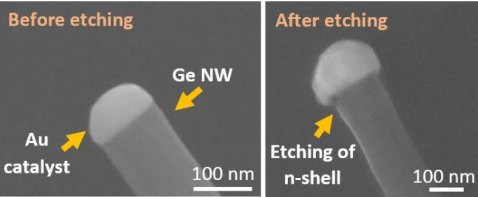
is 1:2. To proceed, the as-grown NWs on Si (111) substrate was dipped in the etchant for 20 s and then rinsed in DIW for 20 s, followed by N2 blow dry. Figure 3.4 shows SEM images of the
n-doped Ge NWs before and after the hydrogen peroxide etching process. As can be observed at the gold catalyst position, about 20 to 30 nm of Ge shell was removed from the NW.
26
Figure 3.4: SEM images of the n-doped Ge NWs before and after the hydrogen peroxide (H2O2) etching process.
The etching process was done by dipping the sample in diluted H2O2/DIW as ratio of 1:2 for 20 s and then DIW for
20 s, followed by N2 gas blow. After the etching, about 20-30 nm of the n-doped shell was removed.
3.3.3 HI Acid Etching of GeO2 Shell
Unlike the stable SiO2 shell, which is typically removed by buffered HF acid, GeO2 is water
soluble. In practice, GeO2 is often removed by hydrohalogenic acids such as HCl, HBr or HI. From
the study of Onsia et al [71], it has been shown that HBr and HI are the best solutions for etching GeO2. Figure 3.5 shows the XPS spectrum of the Ge wafer surface after a treatment by different
hydrohalogenic acids for 5 min. The peak at 30 eV shows the binding energy of Ge bulk. The peak around 33 eV shows the presence of the germanium oxide GeO2. Clearly, there is still GeO2
remaining after HF and HCl acid etching while HBr and HI acid show a good etching result.
Figure 3.5: The XPS spectrum [71] of the Ge wafer surface after being etched by different hydrohalogenic acids for
5 min. The peak at 30 eV indicates the binding energy of Ge while the peak at 33 eV corresponds to the position of GeO2.
27 In our experiments, hydriodic acid (HI acid, >57%, Sigma-Aldrich-MERCK [72]) was used for removing the GeO2 shell around the NW. The sample was dipped in diluted HI/DIW with the ratio
of 1:5 for 5 s and then rinsed in DIW for 20 s to remove all the residual chemicals and subsequently dried by blowing N2 gas. After the etching process, the sample should be transferred immediately
to the deposition chamber that is then pumped to create a vacuum to avoid re-oxidation.
3.3.4 Atomic Layer Deposition (ALD)
The downscaling of modern technologies has led to the requirement for atomic scale control of thin film deposition. Compared with the common physical deposition processes like evaporation or sputtering, which have a high growth rate, atomic layer deposition (ALD) is a chemical vapor deposition technique with high accuracy and repeatability [73]. The depositing process is electrically controlled with the growth rate of Å/cycle. It is possible to deposit on different types of thermally fragile substrates such as inorganic, polymeric, or biological materials by using low-temperature ALD [74]. As the mainstream of modern microelectronics is shifting to nanoscale devices, ALD is thus highly required for depositing ultrathin high-k dielectric materials [75] such as Al2O3, HfO2 or ZrO2. ALD offers an excellent step coverage and conformal deposition on high
aspect ratio structures based on sequential, self-limiting reactions. The process is based on alternate pulsing of the precursor gases and vapors onto the substrate surface and subsequent chemisorption or surface reaction of the precursors. A Quartz crystal microbalance (QCM) is used to examine the deposition processes.
In our experiments, we have deposited 5 nm or 20 nm of Al2O3 shell on the n-doped Ge NWs and
Si0.67Ge0.33 NWs, respectively, to passivate the NW surface. The Al2O3 coating process was
performed using H2O and Al(CH3)3 [trimethylaluminum (TMA)] based on two reactions:
(A) Al-OH* + Al(CH3)3 → Al-O-Al(CH3)2* + CH4
(B) Al-CH3* + H2O → Al-OH* + CH4
The mechanism of Al2O3 growth based on self-limiting reactions is illustrated by the schematic in
28
Figure 3.6: Schematics of self-limiting reactions in ALD technique for Al2O3 deposition using H2O and Al(CH3)3
[trimethylaluminum (TMA)].
The deposition process is repeated for several cycles to obtain the desired thickness. Figure 3.7 shows the HAADF STEM image of the passivated Si0.67Ge0.33 NW covered by 20 nm Al2O3 shell.
For the ALD deposition, the substrate temperature was kept at 250 oC and the peak pressure of H2O
and TMA pulse were set at 2 Torr and 0.8 Torr respectively, giving 20 nm of Al2O3 thickness after
200 cycles.
Figure 3.7: HAADF STEM image of a Si0.67Ge0.33 NW with 20 nm Al2O3 shell deposited by ALD technique. The
29
3.4 Ebeam Lithography
Electron Beam Lithography (EBL) is a fundamental technique in nanofabrication, allowing to transfer a two dimensional (2D) electronic pattern to a substrate using subsequent processes. The NW contacting process contains four main steps, including the dispersion of the NWs on the Si3N4
membrane, spin coating of a photoresist, the exposure of the resist and the development step. An extra step of plasma cleaning is also useful to remove residual resist after the development step. After metal deposition the ‘lift off’ step removes all the resist, including the metal deposited on the resist. Only the metal deposited directly on the sample surface should remain.
3.4.1 NWs Dispersion
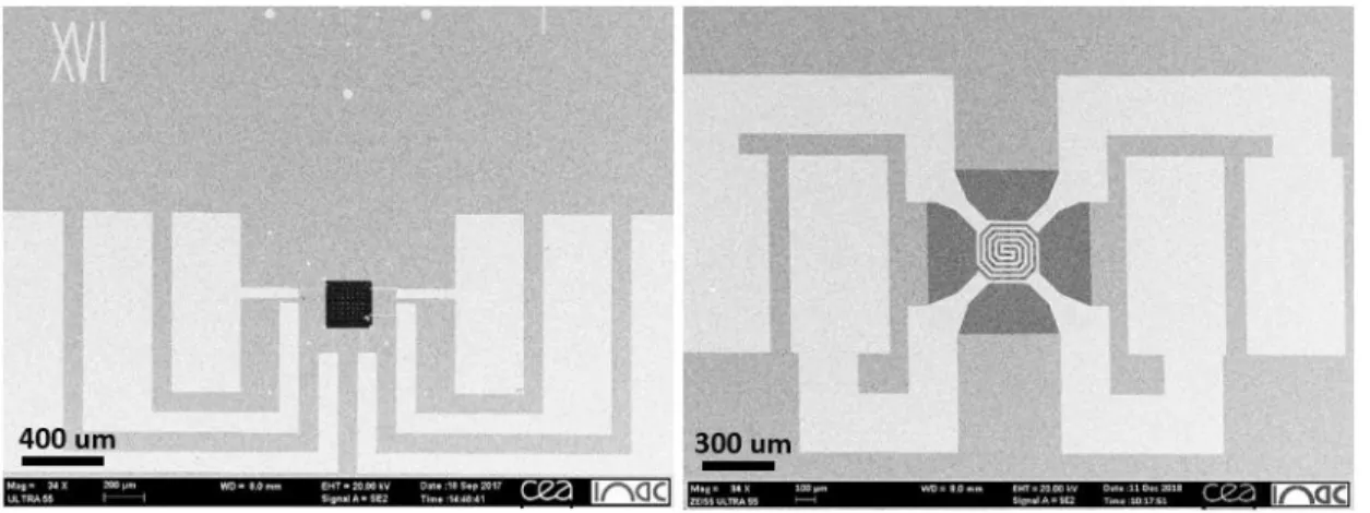
The EBL process starts with the transfer of the as-grown NWs to a substrate. In our experiments, for the TEM investigation, we have dispersed the NWs either on the home-made 200 nm thick electron transparent Si3N4 membrane (Fig. 3.8a) or the temperature calibrated heater chips
from DENSsolutions company (Fig. 3.8b) [22]. Rectangular holes are present in both types of membrane. Additionally, NWs were also dispersed on home-made 40 nm thick electron transparent Si3N4 membranes without holes, to which we refer as ‘flat’ membranes. The fabrication process
for the home-made Si3N4 membrane was described in ref [76]. Particularly shown in figure 3.8a,
the membrane has 6 large gold or platinum electrodes for outer electrical connection and a 200 μm x 200 μm electron transparent Si3N4 window at the center of the membrane (see Fig. 3.9a) used for
the TEM observation. The NWs are randomly dispersed on the Si3N4 window and connected to
outer electrodes via the thin gold inner electrodes using electron beam lithography. For the temperature calibrated heater chips (Fig. 3.8b), a buried metal spiral of well-defined dimensions is present in the center of a 400 nm SiNx membrane that is commercialized by DENSsolutions. The
30
Figure 3.8: SEM images of (a) home-made 200 nm thick electron transparent Si3N4 membrane and (b) the
temperature calibrated heater chips from DENSsolutions company.
To begin the NW contacting process, the substrate containing the as-grown NWs is first separated into around 3 mm x 3 mm pieces and immersed in ethanol solution (in a small plastic container). A moderate sonication step is applied to the plastic container for about 20 s to break the NWs from the substrate. Droplets of the NW solution taken by a micropipette are spread on the Si3N4
membrane followed by N2 blow-drying. Depending on the density of the as-grown NWs on the
growth substrate, the dispersion step can be repeated one or several times. The NW density is verified by optical microscope observation until the expected NW position and density on the membrane is achieved. If there are holes on the membrane (shown in Fig. 3.9), the NWs are attracted to move into the holes giving higher NW density of suspended NWs. It is very interesting to obtain suspended NW structures, to get rid of the influence of the Si3N4 substrate. This is
beneficial both for EDX measurements as well as field mapping techniques such as electron holography [77]. However, the non-uniform coating of the resist layer caused by the holes can increase the risk of lift-off problems. For the NW dispersion on the calibrated heater chip, since the size of the chip is quite small, it is advised not to use N2 gas for blow-drying, but letting the
membrane dry gradually on a hot plate (at ~70 oC) to achieve high NW density on the membrane. After that, SEM images of the dispersed NWs are made to localize the NWs and making the designed patterns using Klayout [78] or Elphy software.
31
Figure 3.9: (a) SEM image of NW dispersion on the Si3N4 window and (b) a zoom on the yellow rectangular box
showing the 2 μm x 8 μm holes and markers with Ge NWs lying over the holes.
3.4.2 Spin Coating of Resist
To facilitate the spin coating of the resist and also to avoid the breaking of the thin Si3N4
membranes by the vacuum pressure, it is advised to glue the membranes on top of a Si wafer using orange Kapton tape. The sample is then spin coated by PMMA 4% (positive photoresist) and baked at 180 oC for 5 min. Depending on the thickness of the deposited metal, the thickness of the photoresist should be adjusted to have a good lift-off. Normally, the thickness of the deposited metal should be less than 1/3 of the resist thickness for a good lift-off. In our experiments, in order to perform the Al metal contacts to 100 nm n-doped Ge NWs, we have deposited 150 nm Al metal layer. The resist thickness required for a good lift-off is about 500 nm, which could be done by two times of the PMMA 4% spin coating with the recipe presented in the table 3.1.
Table 3.1: Recipe for the spin coating process using PMMA 4% as photoresist
Resist
Spin coating Bake Thickness
(nm) Velocity (rpm) Acceleration (rpm/s) Time (s) Bake (oC) Time (min) PMMA 4% 4000 4000 30 180 5 250
To contact larger NW diameters (for instance, Si0.67Ge0.33 alloy NWs with the diameter ranging
from 65 to 250 nm), the metal thickness should be large enough to assure a good coverage of the NW surface. In this case, we have performed three times of PMMA 4% spin coating for 750 nm resist thickness, and then deposited 300 nm of Al metal.
32
3.4.3 Exposure of Resist
The exposure of the resist is performed on the ZEISS LEO1550 SEM working at 20 kV. First, the drawings made using the Klayout software are loaded in the machine and opened (with Elphy software) for the 2D patterning. Then markers pre-patterned on the Si3N4 are used for doing
a calibration of the writing field and correction of the shift and rotation of the writing field. Then the focused electron beam raster scans the field of 300 μm x 300 μm on a membrane with a beam current of ~30 pA and deposits an electron dose of 375 μC/cm2. The step size of the scanning
should be below 2 nm/s. Since the exposure to the electrons of the photoresist will influence its properties, it is advised not to expose the membrane by focusing directly on the writing field or taking images at slow scan-speed.
3.4.4 Development
After the exposure, the sample is dipped in MIBK/IPA 1:3 [methyl isobutyl ketone/isopropyl alcohol] for 55 s (for 500 nm thick photoresist) and then IPA for 1 min to remove the developer. If the thickness of the photoresist is about 750 nm, the development time should be about 80 s. Since the resist is sensitive to white light, it is advised to cover the samples by aluminum foil for transferring to the metal deposition step (that is performed in another cleanroom). Figure 3.10 illustrates four basic steps for NWs contacting using electron beam lithography.
Figure 3.10: four basic steps of NWs contacting process including the dispersion of NWs, the spin coating of resist,
the exposure of the resist at well-defined locations and the development step removing the resist where it has been exposed to the electron beam.
33
3.5 Buffered Oxide Etching (BOE)
Buffered oxide etch (BOE), also known as buffered HF or BHF, is a commonly isotropic etchant in nanofabrication used to remove amorphous SiO2, Al2O3 or Si3N4 [79]. Buffered HF is
a strong acid, highly corrosive and toxic. Due to the risks of BOE appropriate safety measures need to be taken for handling: wearing full protective clothing including boots, safety goggles and/or a full face-shield and gloves of PVC or neoprene is recommended. In our experiments, buffered hydrofluoric acid [80] - BOE 7:1 (HF : NH4F = 12.5 : 87.5%) was used to remove the protecting
Al2O3 shell that covered the NW surface at the location where the Al contact pad would be
deposited in a subsequent fabrication step. The recipe for Al2O3 etching is presented in table 3.2.
Table 3.2: Information for Al2O3 etching using buffered hydrofluoric acid
Buffered HF has a negative side effect on the etching process that the F- ions diffuse underneath the layer of resist and etch the substrate causing ‘resist peeling’ or ‘under-etching’ effects as demonstrated in figure 3.11.
Figure 3.11: Demonstrations of poor adhesion of the resist (left) and isotropic etching of the substrate (right) by
using HF acid solution.
Figure 3.12 shows the HAADF STEM image of the contacted Si0.67Ge0.33/Al2O3 core shell NW
etched by buffered hydrofluoric acid. As indicated by the orange arrows, not only the Al2O3 shell
but also the Si0.67Ge0.33 core has been etched by the buffered HF acid. The HF etching was also
extending underneath the resist layer over a distance of around 500 nm. In addition, due to the use Al2O3 thickness (nm) Time (s) DIW (s) Air blow
5 10 20 N2
34 of a Si3N4 membrane, the buffered HF etching process thins down the membrane increasing the
risk of breaking the membrane during the lift off process. To reduce these negative effects, it is advised to rinse the sample with DIW carefully to remove the HF residual acid and also reduce the HF etching time by depositing a thinner Al2O3 shell (<10 nm).
Figure 3.12: HAADF STEM images of the Al contacted Si0.67Ge0.33 NWs with 20 nm Al2O3 shell showing the
etching of SiGe NW underneath the Al contact pad and the extension of Al2O3 etching below the resist.
3.6 Al Deposition
In this section, we will describe the process of Al metal deposition using sputtering and electron beam evaporation techniques. Some typical characteristics of the two methods are also given. Besides, prior to the metal deposition process, an additional step of soft plasma cleaning will be applied and discussed for the removal of impurities and contaminants on the contact surface.
3.6.1 Ar Plasma Cleaning
Ar plasma cleaning is a common technique used to remove organic contaminations via ion bombardment without causing a chemical reaction or oxidation on the surface of the substrate [81]. The plasma is created using high frequency voltages (typically kHz to >MHz) to excite gas atoms to higher energy states and become ionized. The atoms are then relaxed to lower energy levels and emit photons resulting in the characteristics “glow” or “purple – blue” light associated with plasma. The cleaning process is considered as environmentally friendly since there are no harsh chemicals involved. During our sample fabrication process, after installing the specimen in the evaporation or sputtering chamber for vacuum protection (10-6 Torr), a soft Ar plasma cleaning (250 V) is
35 applied for 15 s. The chamber is then pumped to 10-6 Torr to remove the Ar gas, preparing for the Al deposition step.
3.6.2 Al Deposition by Sputtering and Electron Beam Evaporation
Sputtering and electron beam evaporation are common physical thin film deposition techniques in nanofabrication [82]. A wide range of materials such as metals, insulators, alloys and composites can be used as the target [83]. For the sputtering technique, gas atoms (commonly argon) are excited by a high bias voltage and directed to make collisions to the target (cathode - negative electrode). Since the ions carry high energy, they can transfer their energy and knock out the target atoms, which are then deposited on the substrate arranged in the opposite direction. The ejected target atoms that have received energy from the ion bombardment, will deposit on the substrate with good adhesion and uniform stoichiometry. However, during the sputtering process, the plasma must be maintained in the chamber causing also some deposition of the gas atoms in the thin film. For electron beam evaporation, the electron beam emitted from a hot filament is directed to the target by a magnetic field. The electron beam heats up the target vaporizing atoms, which then precipitate on the substrate placed opposite to the target. For both techniques, the substrates are usually rotated for a uniform coverage and can be heated or tilted to obtain the desired deposition. Figure 3.13 illustrates the mechanisms of the sputtering and electron beam evaporation techniques.


![Figure 4.5: Schematic illustration of different components in a TEM microscope. Ref [94]](https://thumb-eu.123doks.com/thumbv2/123doknet/12890878.370631/55.918.285.695.381.988/figure-schematic-illustration-different-components-tem-microscope-ref.webp)
