HAL Id: cea-03158876
https://hal-cea.archives-ouvertes.fr/cea-03158876v2
Submitted on 17 Mar 2021
HAL is a multi-disciplinary open access
archive for the deposit and dissemination of
sci-entific research documents, whether they are
pub-lished or not. The documents may come from
teaching and research institutions in France or
abroad, or from public or private research centers.
L’archive ouverte pluridisciplinaire HAL, est
destinée au dépôt et à la diffusion de documents
scientifiques de niveau recherche, publiés ou non,
émanant des établissements d’enseignement et de
recherche français ou étrangers, des laboratoires
publics ou privés.
A RISC-V ISA extension for ultra-low power IoT
wireless signal processing
Hela Belhadj Amor, Carolynn Bernier, Zdenek Prikryl
To cite this version:
Hela Belhadj Amor, Carolynn Bernier, Zdenek Prikryl. A RISC-V ISA extension for ultra-low power
IoT wireless signal processing. IEEE Transactions on Computers, Institute of Electrical and
Electron-ics Engineers, 2021, 2021, pp.1-1. �10.1109/TC.2021.3063027�. �cea-03158876v2�
A RISC-V ISA Extension for Ultra-Low Power
IoT Wireless Signal Processing
Hela Belhadj Amor, Carolynn Bernier and Zden ˇek Pˇrikryl
Abstract—This work presents an instruction-set extension to the open-source RISC-V ISA (RV32IM) dedicated to ultra-low power (ULP) software-defined wireless IoT transceivers. The custom instructions are tailored to the needs of 8/16/32-bit integer complex arithmetic typically required by quadrature modulations. The proposed extension occupies only 2 major opcodes and most instructions are designed to come at a near-zero energy cost. Both an instruction accurate (IA) and a cycle accurate (CA) model of the new architecture are used to evaluate six IoT baseband processing test benches including FSK demodulation and LoRa preamble detection. Simulation results show cycle count improvements from 19% to 68%. Post synthesis simulations for a target 22nm FD-SOI technology show less than 1% power and 28% area overheads, respectively, relative to a baseline RV32IM design. Power simulations show a peak power consumption of 380 µW for Bluetooth LE demodulation and 225 µW for LoRa preamble detection (BW = 500 kHz, SF = 11). Index Terms—RISC-V ISA extension, IoT, software-defined radio, ultra-low power (ULP) transceiver architecture, Bluetooth, LoRa.
F
1
I
NTRODUCTIONW
IRELESS Internet of Things (IoT) connectivity solu-tions have been gaining exponential adoption rates and enabling new applications in a diverse range of verticals such as transportation, health, industry and agriculture. The huge diversity of IoT use cases has naturally spurred the de-velopment of dedicated communication protocols, from the physical layer to the networking layers. Indeed, since IoT endpoints are typically energy constrained devices, tailor-ing the communication protocol to an application’s specific needs is a necessity, amplified by the fact that transmitting data is often the principal energy expenditure in the applica-tion’s power budget. Thus, a wide variety of communication protocols have been proposed, each targeting a unique set of specifications: communication range, data bandwidth, power consumption, latency, up/down-link transmission requirements, target transceiver cost, and so on. Focusing on the physical layer (PHY), this has led to the emergence of a large number of IoT standards (and families of standards) such as RFID, Bluetooth, LoRa, Sigfox, EnOcean, Narrow-Band IoT, EC-GSM, LTE-M, IEEE 802.15.4-2015, IEEE 802.11, etc.Within this huge application space, many battery-powered and energy harvesting IoT solutions require ultra low-power integrated circuits (IC), and in particular in the wireless transceiver subsystem. To reach this goal, these circuits have until now mostly been implemented using dedicated hardware designs. Unfortunately, this leads to designs with very limited wireless reconfigurability, an im-portant drawback in the context of quickly evolving IoT standards. Proprietary communication systems or those that are dedicated to long in-field deployment life-times, such as industrial or satellite IoT, also require reconfigurability to
• Hela Belhadj Amor is now with Dolphin Design, Grenoble, France.
• Carolynn Bernier is with the Digital Systems and Integrated Circuits De-partment of CEA, LIST, Grenoble, France. Email: [email protected]
• Zdenˇek Pˇrikryl is with Codasip s.r.o., Brno, Czech Republic. Manuscript received ; revised .
adapt to changing protocol requirements. Finally, hardware transceivers leave little room for PHY-layer experimentation which is necessary to drive innovation in the field of next-generation radio protocols.
Thanks to the important improvements in performance, cost and power consumption of DSP and FPGA technolo-gies, new software-defined radio (SDR) applications have recently emerged [1]. For example, authors in [2] and [3] use FPGA platforms to build agile cellular transceivers, from 3G to 5G. The recent development of small and nano-satellite systems has spurred interest in SDR for space-borne multimode transceivers [4], [5], [6]. Closer to our application, authors in [7] propose a reconfigurable IoT gate-way able to address the multiplicity of IoT communication standards. Unfortunately, the power consumption figures of such systems, which typically couple a DSP and/or FPGA chip for baseband and/or digital front-end processing with an RF/analog front-end chip, are orders of magnitude above those required by most IoT endpoints. This is due both to the energy cost of transmitting signals between integrated circuits but also, and more importantly, to the fact that these circuits generally offer too much reconfiguration potential and are therefore over-specified for energy constrained IoT nodes.
A single-chip software-defined radio-frequency (RF) transceiver is therefore highly desirable provided it respects the power budget of the IoT wireless subsystem. While unfeasible until now, several current trends, including the heterogeneous multi-core paradigm and the uptake by in-dustry of the easily extendable open source RISC-V ISA [8], along with the continued improvements in CMOS scaling, concur to show that this idea’s time has come.
To this end, this work makes the following contributions:
• We identify the digital processing requirements typi-cal of IoT wireless baseband signals;
• We propose an instruction set extension for the RISC-V ISA tailored to the needs of wireless DSP and that
2
Fig. 1: Simplified architecture of softwadefined RF re-ceiver (reproduced from [9])
achieves high cycle count reductions with ‘near zero’ power overhead;
• Based on this new instruction set, a core dedicated to
wireless DSP and that is fast and powerful enough to process complex sample streams in real-time while consuming only a fraction of the power of the com-plete ULP transceiver subsystem is designed;
• IoT protocol test bench simulations show important cycle count improvements with more than 50% ob-tained for the LoRa demodulation algorithm;
• Power consumption estimations based on post-synthesis simulations of the proposed core prove the feasibility of ultra-low power for two of the most popular IoT wireless protocols, Bluetooth LE and LoRa, and this even for one of the most computationally-intense versions of the LoRa proto-col (SF = 11, BW = 500kHz). This is achieved even without dynamic voltage scaling.
We believe that our work paves the way to making ultra-low power software-defined radio a reality.
The rest of the paper is organized as follows: in Sec-tion 2, we discuss related work in the fields of ULP wireless signal processors and instruction set extensions for DSP. In Section 3, we discuss the properties of wireless DSP and the opportunity offered by the RISC-V ISA. In section 4, we present a RISC-V ISA extension for IoT signal processing. Six wireless test bench algorithms are described in Section 5 and evaluation results using the proposed architecture are presented in section 6.
2
R
ELATEDW
ORK2.1 Processors in the IoT landscape
In an embedded IoT platform, the application processor is responsible for executing the IoT application’s task, e.g. read, store, process and decide when to transmit the sensor data. The large diversity of IoT applications and their often extreme demands in terms of power efficiency has spurred the development of a wide range of application processors. Even if we limit the discussion to those employing a variant of the RISC-V ISA, it is possible to find IoT processors targeting a power consumption in the nW range for battery-less applications [10], cores targeting the µW and mW range [11], cores specifically designed for flexibility over the 2-200 MHz range [12], and multi-core platforms targeting computing intensive edge applications [13].
In addition to this diversity, a recent trend has con-sisted in the development of heterogeneous, multi-core IoT platforms [11], [14], [15], [16] capable of offloading specific, high intensity tasks from the main application processor (e.g. security features, deep learning algorithms).
Since the processing of wireless signals is particularly de-manding (to the point where it has historically typically been done using dedicated hardware), the trend towards heterogeneous multi-core platforms is an opportunity which can potentially also be seized by software-defined wireless transceivers. The challenge of developing such a tailor-made core capable of meeting the hard real-time constraints and high complexity of wireless DSP in an ultra-low power context is the focus of this present work.
2.2 A tailor-made core for ULP wireless DSP
If, traditionally, the digital processing blocks in ULP transceivers have been implemented using dedicated or reconfigurable hardware, replacing these blocks by a pro-cessor implies carefully studying the energy cost of moving to software. This move to software has long been studied in high-end communication systems such as cellular and high data-rate systems where the flexibility required to address multiple communication standards has been a long-time requirement [17], [18], [19].
For ULP transceivers, where the power budget allowable to the processing of the digital baseband (DBB) signals is on the order of hundreds of µW to a few mW, the need for flex-ibility has partly been addressed by reconfigurable designs compatible with a limited number of wireless standards, typically two or three, often by sharing hardware blocks [20], [21], [22], [23]. Thus the ULP design space is still far from having achieved the flexibility offered by the software defined radio (SDR) paradigm, limiting the deployment potential of a given design in terms of addressable standards but also limiting the potential to create and deploy new digital baseband algorithms.
Conscious of this need, dedicated micro-architectures for ULP SDR have recently been proposed by [24] and [25]. To achieve ultra-low power, both of these approaches focus on the reduction of the SDR processor’s working frequency. To this end, [24] proposes an architecture based on a cus-tom Single Instruction Multiple Data (SIMD) unit, with a datapath that can be reduced to very small bit widths (4 or 8 bits), associated to a scalar unit. A different approach is explored in [25] which presents a 32-bit scalar architec-ture with application-specific instructions that reduce the number of required instructions from 10 to 4 for a typical frame detection algorithm. In both of these works, the choice of designing a dedicated machine implies that algorithms must be hand-coded in machine specific assembly code. This excludes the reuse of widely available software tool chains and DSP libraries. An alternative approach was pro-posed in our previous work [9] with a strategy based on small general purpose micro-architectures (including RISC-V). Thanks to advanced CMOS scaling and sufficiently high clocks, we showed that a timing and power consumption performance compatible with ULP IoT protocols can be achieved on these platforms, even without voltage scaling. However, these results were obtained for a relatively simple, mostly real-valued wireless test bench. Other IoT signaling protocols require higher computational resources due to the extensive use of complex signals. To address these higher complexity protocols, this present work exploits processor ISA customization.
A tailor-made core for ULP SDR therefore must be fast and powerful enough to process, in real-time, the complex sample stream produced (in RX) or required (in TX) by the transceiver front-end, while consuming only a fraction of the power of the complete transceiver subsystem, i.e. on the order of hundreds of µW to a few mW. To take advantage of the variations of complexity over time, the core must be able to put itself to sleep, ideally in a single cycle, while waiting for the next available block of samples. To further minimize power, the ROM section of the core’s TCM (Fig. 1) should be implemented using either low-retention-current SRAM or using a high-speed embedded non volatile technology. In this way, the core’s voltage supply can be switched off between successive frame transmissions (relatively rare in IoT systems). This also means that the core does not need to be optimized for leakage.
2.3 Instruction set extensions for DSP
While the idea of extending the ISA of a processor to customize for a specific application is not new, in each case, the challenge consists in finding the optimal set of useful in-structions. In the ultra-low power context which is ours, the challenge is further increased by ensuring that the proposed set comes at a near-zero power cost. Finally, the hard real-time constraints specific to wireless DSP must imperatively be met, implying that the speed burden imposed by the larger extended core must be acceptable.
The RISC-V instruction set architecture (ISA) is a stan-dardized and open architecture specifically designed to support extensive user-level ISA extensions and specialized variants [8]. The RISC-V ISA is defined as a base integer ISA, which must be present in any implementation, plus optional standard and non-standard extensions. The base ISA is care-fully restricted to a minimal set of instructions allowing for extremely energy efficient hardware implementations. Thus, highly energy efficient application-specific processors can be designed by adding a set of carefully chosen extensions, either standard or non-standard, to the base ISA. Partial customization of a standard ISA lowers the design effort to develop the necessary software tools, allows the use of a known, well tested architecture as a starting point to the new design and simplifies the reuse of existing DSP libraries.
For these reasons, the authors in [26] propose a RISC-V extension to the RRISC-V32IM ISA (32-bit integer base ISA with multiplication extension) for SDR. Similarly as in this work, the authors propose a set of custom instructions to accelerate complex-number arithmetic. To represent the real and imaginary parts of a complex number without changing the addressing mode and data width, 32-bit complex-data words are considered vectors of two 16-bit words. While the authors propose a number of instructions that are use-ful in typical complex DSP algorithms, such as complex ADD/SUB/MUL as well as complex radix-2 butterfly, this last being extensively used in FFT algorithms, the need for instructions such as CSMUL (complex-scalar multiply), CONJ (complex conjugate) or packed 8-bit arithmetic are questionable, as will be discussed below. By limiting the dynamic range of their instructions to 16 bits, the authors limit the applicability of their extension to low to medium
sensitivity protocols. Finally, no discussion on the impact of these new instructions on the processor’s power consump-tion is provided.
At the time of this writing, the RISC-V community is considering the standardisation of a ”P” extension intended for DSP acceleration and which includes packed-SIMD in-structions targeting the segmentation of the integer registers into either two 16-bits or four 8-bits words. Packed-SIMD instructions require modifying the ALU to simultaneously work on vectors of two or four elements. Unfortunately, typical DSP ISA extensions, such as the one provided by [27] have a large instruction count, potentially larger than the base RISC-V ISA, implying a prohibitive energy cost. And of this large number of instructions, many are of little practical use in RF algorithms, as will be discussed below.
An alternative RISC-V extension is proposed in [28] targeting the processing of IoT real sensor data. The number of additional instructions is intentionally limited in order to minimize the impact on the core’s power consumption (only +9% overhead with respect to the base RISC-V design.) As discussed at length in our previous work [9], the vectorial hardware extensions proposed are of limited interest for complex (versus real) data and the proposed hardware loop mechanism can rarely be used in our algorithms which typically contain conditional branches. However, for completeness, we included comparative results using this architecture in Tables 3 and 5. Our work in [9] also contains a detailed analysis of the advantages of RISC-V-based archi-tectures over ARM-based ones for our targeted application.
3
W
IRELESSB
ASEBANDD
IGITALS
IGNALP
RO-CESSING
In this section, we introduce the background information related to wireless digital signal processing necessary for understanding the design strategy developed in Section 4. Indeed, a deep understanding of the requirements of such algorithms is required to design a minimal set of useful instructions.
3.1 Software-defined ULP receiver architecture
Focusing on the receiver, which is computationally more complex than the transmitter, a software-defined RF ar-chitecture for ULP IoT signaling schemes is proposed in Figure 1. Indeed, while IoT PHY protocols differ in terms of modulation, signaling rate, coding scheme, etc., narrow-band signaling schemes, i.e. occupying a maximum ana-log bandwidth on the order of a few MHz, share simi-lar characteristics thus allowing the use of reconfigurable dedicated circuits in the RF, analog and digital front-end (DFE). The DFE performs filtering, decimation, optional down-conversion from an intermediate frequency (IF) and automatic gain control (AGC).
However, the wide variety of modulations and signaling schemes pleads for a software implementation of the base-band DSP operations required by each protocol.1Placing the
1. Other important parts of physical layer receiver algorithms (de-interleaving, decoding, CRC, etc.) are not addressed in this work since they operate on demodulated data. Indeed, a DBB processor with a high frequency clock should be able to handle the delay specifications of these algorithms without difficulty.
4
TABLE 1: Proposed ISA Extention for Wireless DSP
Mnemonic Instruction Operation
ADDC16 rd, rs1, rs2, imm 16-bit Addition & Shift Right rd.L = (rs1.L + rs2.L)>>imm Arithmetic Immediate rd.H = (rs1.H + rs2.H)>>imm SUBC16 rd, rs1, rs2, imm 16-bit Subtraction rd.L = (rs1.L - rs2.L)>>imm
rd.H =(rs1.H - rs2.H)>>imm CRASC16 rd, rs1, rs2, imm 16-bit Cross Add & Sub rd.L = (rs1.L + rs2.H)>>immrd.H = (rs1.H - rs2.L)>>imm CRSAC16 rd, rs1, rs2, imm 16-bit Cross Sub & Add rd.L = (rs1.L - rs2.H)>>imm rd.H = (rs1.H + rs2.L)>>imm SRAC16 rd, rs1, rs2 16-bit Shift Right Arithmetic rd.H = rs1.H>>rs2rd.L = rs1.L>>rs2 SRAIC16 rd, rs1, imm 16-bit Shift Right Arithmetic Immediate rd.L = rs1.L>>imm rd.H = rs1.H>>imm SLLIC16 rd, rs1, imm 16-bit Shift Left Logical Immediate rd.L = rs1.L<<imm
rd.H = rs1.H<<imm
MUL2ADD16-32 rd, rs1, rs2, imm Two ”16x16” and Signed Addition rd = [(rs1.L * rs2.L) + (rs1.H * rs2.H)]>>imm
MULC8-16 rd, rs1, rs2, H1, H2, C, imm
if C=0: 8-bit complex multiplication, if Hx = 1,{ix,qx}={rsx.B2,rsx.B3}
conj=1 if Hx = 0,{ix,qx}={rsx.B0,rsx.B1}
if C=1: 8-bit complex conjugate multiplication, rd.L = (i1 * i2 - conj * q1 * q2)>>imm conj=-1 rd.H = (i1 * q2 + conj * i2 * q1)>>imm MULC16 rd, rs1, rs2, C if C=0: 16-bit complex multiplication, rd.L = (rs1.L*rs2.L)>>16 - conj*(rs1.H*rs2.H)>>16
conj=1
if C=1: 16-bit complex conjugate multiplication, rd.H = (rs1.H*rs2.L)>>16 + conj*(rs1.L*rs2.H)>>16 conj=-1
MULC16-32 rd1, rd2, rs1, rs2, C if C=0: 16-bit complex multiplication,conj=1 rd1 = (rs1.L * rs2.L - conj * rs1.H * rs2.H) if C=1: 16-bit complex multiplication, rd2 = (rs1.H * rs2.L + conj * rs1.L * rs2.H)
conj=-1
if rs = 0, rd = 0 CLRSB rd, rs Count leading redundant sign bits if rs > 0, rd = clz (rs) - 1
if rs < 0, rd = clz (∼rs) - 1 PACK-INIT rs Initialize packing barrel-shifter r sh pack = rs
Pack a 16 bit complex value on 32 bits Ival = rs1 << r sh pack PACK rd, rs1, rs2
after removing r sh pack redundant sign bits Qval = rs2 << r sh pack rd = Qval[31:16] :: Ival[31:16] Shorthand definitions:
r.B3→r[31:24], r.B2→r[23:16], r.B1→r[15:8], r.B0→r[7:0], r.H→r[31:16], r.L→r[15:0]
“∼” is bitwise not, “::” is concatenation, “clz” returns the number of leading zeros of an unsigned 32-bit value.
hardware/software frontier at the output of the DFE also means that the digital baseband (DBB) processor operates on sample streams that have been well decimated from the ADC’s high sampling rate. This complex sample stream is produced at a constant sample rate by the DFE and must be processed in real-time since the exact arrival time of a frame is unknown. To this end, communication mechanisms, such as interrupts, sample buffer and feedback control signals, must be inserted between the DFE and the DBB. The high-level features of the ULP receiver architecture are summa-rized in Figure 1.
3.2 Properties of wireless IoT signal processing
At the input of the baseband signal processing algorithm, the quadrature (complex) signal, DBBIn[k] (Figures 4, 5 and 7), has typically been well filtered and decimated. Therefore, in ideal minimum signal-to-noise (SNR) conditions, a signal dynamic range of only a few bits (2 to 4 bits, or approxi-mately 14 to 26 dB) is sufficient for modulations commonly employed in ULP IoT signaling schemes. In practice how-ever, more bits are often required either to address non-ideal demodulation algorithms, but also to allow for front-end imperfection compensation mechanisms. We therefore con-sider that the input signal, represented as signed integers, occupies a dynamic range of 8 bits maximum for each of the in-phase and quadrature-phase components. We also assume that, after the decimation stages of the DFE, the
received signal is over-sampled with typical ratios on the order of 1 to 8.
In wireless DSP, the received signal is often a combi-nation of a small useful signal and a large noise signal, especially when receiving a minimum energy signal (i.e. receiver sensitivity). This means that the useful signal can be contained in the least significant bits of the received signal. Any further quantification of the signal, for example by restricting the normal increase of dynamic range at the output of mathematical operators, can have an important impact on the receiver’s sensitivity. Thus, when mapping a wireless DSP algorithm onto a programmable platform with fixed data words of either 8, 16 or 32 bits, the programmer must have a clear view of the evolution of the signal’s dynamic range among the sequence of mathematical oper-ations. Preliminary system-level simulations are required to evaluate the impact on sensitivity of suppressing low order bits, an operation which can add significant quantification noise if applied carelessly. Similarly, care must be taken with high order bits since signal overflows must be avoided at all costs. Indeed, if an overflow occurs, simply dropping it creates important distortion whereas saturation injects non-linearity. In order to avoid wasting precious CPU cycles checking for overflows, system simulations can be used to detect if the probability of overflow is important, e.g. if an additional bit is required at the output of a sum or subtraction operation. Luckily, since signals rarely occupy
the entire dynamic range, this is often not necessary.2 In
the following, we propose mechanisms for performing both static and real-time dynamic range adjustments.
Concerning the evolution of dynamic range, a general observation is that the very first mathematical operation in a wireless baseband DSP algorithm is often a complex multiplication, e.g. a correlation with a reference signal. In many algorithms, a second multiplication quickly follows, leading to a signal dynamic range that quickly reaches 32 bits with little possibility for later reducing it back to 8 or 16 bits unless automatic gain control is used to ensure that the useful signal occupies the entire targeted dynamic range. For this reason, in the proposed extension, the only instruction which addresses 8-bit data is a complex mul-tiplication instruction. Finally, we observe that, if a SIMD instruction has equal input and output dynamic range, it can only be used in very specific parts of the wireless DSP algorithm (e.g. FFT computation). The design strategy behind the proposed ISA extension is based on the sum of the considerations presented in this section.
3.3 The RISC-V opportunity for wireless baseband DSP
As shown in the previous section, a 32 bit processor is well adapted to the evolution of signal dynamic range in wireless DSP. The absence of fixed point instructions or FPU also results in extremely low gate-count cores, able to function at high frequency with high energy efficiency. While the RISC-V ISA authorizes many opcode sizes, in our work, only 32 bit instructions are used in order to limit the decoder complexity. In particular, the RV32IM ISA uses only 15 major (7-bit) opcodes, with four major opcodes expressly reserved for custom extensions. This offers considerable flexibility for defining complex instructions thanks to the 25 remaining bits. In the proposed extension, this flexibility is exploited in two ways. The importance of statically controlling the dynamic range of the signal throughout the algorithm is addressed in most of our instructions thanks to the possi-bility of removing bits from the computed result. Opcode flexibility can also be used to define instructions in which there are more than 1 destination register or to add useful control bits.
3.4 Exploring the instruction jungle
In order to avoid needlessly increasing the core’s size and complexity, many instructions which might have some util-ity in certain algorithms were excluded when they did not seem clearly indispensable. Here, we review a number of instructions that have been proposed in the related literature and which were rejected for the reasons described below.
General purpose DSP extensions such as [27] typically propose a number of variants for each mathematical opera-tor in order to deal with overflows. ‘Halving’ variants, such as RADD, conserve the overflow by dividing the output by 2 (suppressing the LSB). We adopted a more general approach by allowing the suppression of imm bits from the output,
2. The system-level evaluation of the impact of dynamic range ad-justments on performance is specific to each implementation of each given communication standard. It is therefore beyond the scope of this present work.
with the case imm=0 corresponding to dropping the over-flow. Similarly, saturating operators are unnecessary since saturation must be avoided by design, i.e. careful algorithm planning. MIN and MAX instructions were also rejected because, in typical algorithms in which the minimum or maximum value of an array of values is required (e.g. when looking for a correlation peak), the corresponding array index is often also required. Thus the comparison performed by MIN/MAX needs to be performed a second time in order to memorize the index of the running maximum value hence resulting in no performance improvement.
The authors in [26] propose a number of instructions for accelerating complex arithmetic. In particular, a complex-scalar multiply (CSMUL) instruction is proposed. This in-struction was rejected after observing that, in our experi-ence, in cases where the complex signal is multiplied by a real value, the algorithm designer can often opt for power of two multiplications (and divisions) that can better be implemented as shifts. The authors also propose a complex conjugate instruction (CONJ) which we rejected since this operator can easily be substituted either by a sign change in equations or through the use of a control bit in complex multiplication instructions. Also, we observe that the ‘con-ditional branch if less than’ instruction (CBLT) proposed by [25] is already present in RV32I.
Given the constantly decreasing surface/power costs of arithmetic operators in advanced technologies, it is tempt-ing to imagine the possibility of stempt-ingle-cycle 32-bit complex instructions (sum, subtraction, multiplication). This requires duplicating the ALU in order to simultaneously handle real and imaginary 32-bit data. This also requires adding 3 additional 32-bit multipliers in order to perform the four simultaneous multiplications required by the multiplication of two complex numbers. While the corresponding surface increase might seem like an acceptable compromise in view of the expected increased computing efficiency, in prac-tice, this approach suffers from the following limitations: if memory access is 32-bit, computing efficiency is limited by read/write cycles which require two cycles for complex data; reading and writing complex data to the register file in a single cycle impacts the number of input and output ports of this crucial block; and finally, since complex operations require six 32-bit operands which cannot be encoded in a 32-bit opcode, instructions must make implicit assump-tions as to the location of data in the register file. This in turn complicates register allocation. For these reasons, this approach was rejected. Finally, after having carefully considered the pros and cons of each instruction, the needs of our algorithms, and the targeted system specifications, we developed the ISA extension presented below.
4
RISC-V ISA E
XTENSION FORW
IRELESSI
OT
DSP
Since existing ISA extensions are not appropriate for our needs, we adopt a clean slate approach to designing our DSP extension. Our primary driver being the reduction of energy consumption by lowering the number of CPU cycles required to perform a given task, we adopt the following philosophy: we identify the smallest possible set of instruc-tions that are of high value in reducing the cycle count of
6
typical wireless baseband DSP algorithms. In particular, we focus on instructions that come at a low energy/surface cost thanks to the replacement of existing hardware operators by reconfigurable hardware in the execution stage of the pipeline. We propose 14 instructions which can be encoded using only 2 major opcodes, Table 1.
4.1 Complex arithmetic instructions
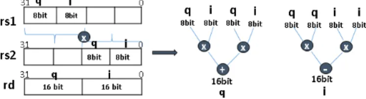
With data that is well adapted to 8, 16 or 32-bit word lengths, we propose a representation of 32-bit data words as vectors of either two complex values {q2, i2, q1, i1} with 8-bit
ele-ments or one complex value {q1, i1} with 16-bit elements,
as illustrated on Figure 2. The existing arithmetic operators of the ALU (adder, barrel-shifter) can easily be reconfigured to perform two simultaneous 16-bit operations rather than a single 32-bit one. Thus, a packed SIMD approach is proposed for complex signed sum (ADDC16), subtraction (SUBC16), crossed sum/subtract (CRASC16), and crossed subtract/sum (CRSAC16), these last being commonly used in FFT butterfly algorithms. Thanks to a reconfigurable barrel-shifter, complex 16-bit shift instructions are also in-cluded: SRAC16 and SRAIC16 perform two arithmetic right shifts filled with the sign-bits Rs1(31) and Rs1(15) whereas SLLIC16 performs two 16-bit logical left shifts.
As discussed previously, in order to avoid losing cycles checking for overflows, we assume that the DSP algorithm designer has a clear view of the signal’s dynamic range requirements at all steps of the algorithm. This assumes, as is commonly performed even for hardware implementa-tions, that preliminary system-level simulations were able to detect the impact of suppressing low and high-order bits at the output of each operator. Thus, to adjust the signal dynamic range as needed, most of our proposed instruc-tions have an immediate operand, imm, which performs an arithmetic right shift of imm LSB bits from the calculated outputs. For maximum flexibility, imm is encoded using 4 or 5 bits for 16 or 32 bit-width data, respectively. To perform this shift operation, we reuse the ALU’s existing recon-figurable barrel-shifter. This additional logic comes with a timing penalty which affects the core’s maximum working frequency. However, as will be shown below, this trade-off is clearly acceptable in view of the avoided dedicated shift cycles.
4.2 Reconfigurable multiplication instructions
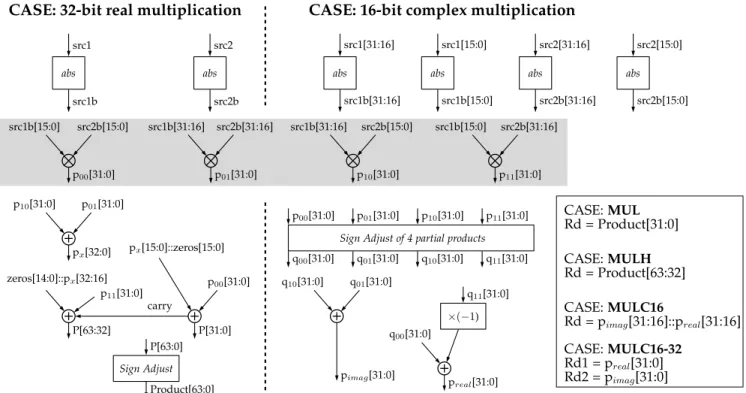
Complex multiplication is one of the most crucial oper-ations in wireless signal processing. To this end, if the existing 32-bit multiplier is replaced by a reconfigurable one (reconfigurable multipliers come at a very low addi-tional energy/surface cost [29]), several useful instructions
Fig. 2: 8x8 bit Signed Complex Multiplication where H1=1 and H2=0
can be proposed which execute, in a single cycle, the six mathematical operations required by a complex multipli-cation. As shown in Figure 3, four partial products, {p00,
p01, p10, p11} are computed whose outputs are combined
differently depending of the multiplication wanted: real or complex. Thus, while still able to perform the multiplication operations of the M extension of RV32 (namely, MUL and MULH), the multiplier can be reconfigured to perform a 16-bit complex multiplication in a single cycle. Note that since all multipliers operate on positive numbers, absolute values and sign adjustments must be calculated prior and after multiplication, respectively. We propose two complex multiplication variants: MULC16 performs four 16-bit mul-tiplications and then retains the 16 most significant bits of the sum or difference of these four products. The 2x16-bit complex result is placed in the destination register. Note that any overflow bit is ignored. The second variant, MULC16-32, performs the same operation but keeps the 32-bit output dynamic range. The two 32-bit results are stored in two destination registers {rd1, rd2}. In order to avoid adding a write port to the register file, these two values are written back in two successive cycles.
While not shown in Figure 3, the reconfigurable multi-plier can also be programmed to execute a MUL2ADD16-32 instruction which performs two signed 16-bit multipli-cations and sums the two 32-bit results. This can be used for example to find the modulus of 16-bit complex values. Finally, the MULC16 instruction performs four signed 8-bit multiplications, a sum and a subtraction in a single operation to produce a 16-bit complex output, as depicted in Figure 2. Bits H1 and H2 select the upper or lower parts of registers rs1 and rs2, respectively. For maximum flexibility, rs1 and rs2 can be the same register. A final useful feature consists in adding the control bit “C” to the three complex multiplication instructions in order to compute the complex multiplication with the conjugate value of the second source operand (rs2).
4.3 Automatic gain control (AGC) instructions
While static (i.e. predictable) signal dynamic range adjust-ments can be performed using the immediate operand, imm, introduced previously, fast dynamic range adjustments of the received signal are often necessary. This is due to the highly dynamic nature of the wireless channel which im-plies highly fluctuating signal and interference levels. This means that, often, the useful signal does not fully exploit the available dynamic range and can even be contained in the least significant bits of a given word. In absence of auto-matic gain control, every matheauto-matical operator must avoid introducing quantification errors, meaning that dynamic range naturally tends to increase. This is particularly true of multiplication operations which approximately double the signal dynamic range. A cascade of several multiplication operations will thus quickly lead to high cycle-count 32-bit complex operations.
While an initial automatic gain control step is often performed in the DFE in order to scale the received signal to the dynamic range available at the DBB input, certain algorithms might require secondary automatic gain control in the DBB. This might be true e.g. if channel filtering is
abs abs abs abs abs abs
src1 src2 src1[31:16] src1[15:0] src2[31:16] src2[15:0]
src1b src2b src1b[31:16] src1b[15:0] src2b[31:16] src2b[15:0]
CASE: 32-bit real multiplication CASE: 16-bit complex multiplication
src1b[15:0] src2b[15:0] p00[31:0] src1b[31:16] src2b[31:16] p01[31:0] src1b[31:16] src2b[15:0] p10[31:0] src1b[15:0] src2b[31:16] p11[31:0] p10[31:0] p01[31:0] px[32:0] zeros[14:0]::px[32:16] p11[31:0] P[63:32] px[15:0]::zeros[15:0] p00[31:0] P[31:0] carry Sign Adjust P[63:0] Product[63:0]
Sign Adjust of 4 partial products p00[31:0] q00[31:0] p01[31:0] q01[31:0] p10[31:0] q10[31:0] p11[31:0] q11[31:0] q10[31:0] q01[31:0] pimag[31:0] ×(−1) q11[31:0] q00[31:0] preal[31:0] CASE: MUL Rd = Product[31:0] CASE: MULH Rd = Product[63:32] CASE: MULC16 Rd = pimag[31:16]::preal[31:16] CASE: MULC16-32 Rd1 = preal[31:0] Rd2 = pimag[31:0]
Fig. 3: Reconfigurable multiplier. (The operator “::” represents concatenation.)
performed in the DBB. While automatic gain control can be performed with existing instructions, we propose three instructions dedicated to speeding up this task. The in-structions provide an additional benefit of dealing with the doubling of dynamic range caused by each multiplication operation. Indeed, since 16 bits represent a comfortable signal to quantification noise ratio of approximately 98 dB and since a packed representation of a single 16-bit com-plex value is perfectly adapted to a 32-bit architecture, we propose to favour the 16-bit data representation during the design of the DSP algorithm. We thus propose to accelerate the task of applying AGC to 32-bit complex data in order to produce packed 16-bit complex data. This means that, if an operator produces complex 32-bit data, these instructions can be used to effectively rescale the data onto a packed 16-bit complex representation, this in order to exploit the 16-16-bit complex instructions proposed previously.
To this end, we introduce three instructions: CLRSB returns the number of redundant sign bits of a signed 32-bit integer within a single cycle. This provides an efficient, low gate-count alternative to an equivalent software implemen-tation. The minimum value returned by the CLRSB instruc-tion executed over a significant number of signal samples represents the available unused dynamic range. Once this measurement has been made, the PACK instruction packs two 32-bit signed values onto a single 32 bit word, while removing the r sh pack most significant bits (excluding the sign bit) and then the 16 LSB of both input operands. The r sh pack register is initialized by a single call to the PACK-INIT instruction.
5
T
ESTB
ENCHD
EFINITIONSIn this section, we present a set of DSP algorithms that are commonly encountered in IoT communication schemes,
including some of the most popular IoT communication standards such as Bluetooth LE [30], LoRa and Sigfox [31]. A bare-metal C version of these algorithms was implemented in order to evaluate the proposed ISA extension.
5.1 Software FSK demodulation
Gaussian frequency shift keying (GFSK) modulation is em-ployed in many IoT physical layers, e.g. in the Sigfox and Bluetooth protocols. Our first test bench is an FSK modu-lated frame synchronization and demodulation algorithm, illustrated on Figure 4 and presented in detail in [9]. This al-gorithm conforms to typical IoT frame detection alal-gorithms in that it consists of (at least) three phases: a Preamble Search phase to detect the frame’s presence, an SFD Search phase to synchronize the receiver to the beginning of the frame’s useful data, and a Demodulation phase which recovers the data symbols. Computational complexity is often highest in the “SFD Search” phase.
In this algorithm, we observe that the first operation applied to the 8-bit input signal DBBIn is a complex mul-tiplication, followed by averaging and IIR blocks. A
mod-z−1 conj. × 1 N OSR−1 P k=0 z−k IIR | | Max. Table Val. Ind. OSR 1 0 =(z) Sign SFD Search Demodulated symbols DBBIn8 16 16 16 32 SFDSearch SFDFound SFDFound SFDFound SFDFound
Fig. 4: Simplified view of FSK demodulation algorithm. Double arrows indicate complex signals. The signal dy-namic range is shown in lighter type (reproduced from [9]).
8
× BaseSeq∗8
FFT Right 3Shift abs()2 IIR ArgmaxVal.
Ind.
DBBIn8 16 16 16 32 32
Index val max
Fig. 5: Simplified view of LoRa preamble detection algo-rithm. Double arrows indicate complex signals. The signal dynamic range is shown in lighter type.
ulus operation extracts the correlation maximum values as well as the corresponding sample indices required to recover the symbol timing. Thus this algorithm can benefit from the proposed MULC8-16, MUL2ADD16-32, ADDC16 and SUBC16 instructions. Several logical signals such as SFDSearch and SFDFound are used to control the different phases of the algorithm. Preliminary Matlab simulations of the fixed-point algorithm were used to evaluate acceptable bit scaling at the output of each mathematical operator. The resulting evolution of signal dynamic range is shown in lighter type.
5.2 LoRa preamble detection
LoRa is a spread spectrum, long range wireless communi-cation protocol that targets ultra low power IoT terminals. In the Frequency Shift Chirp Modulation (FSCM) employed, symbols are encoded as one of N possible frequency offsets of a linear time-varying frequency signal (chirp) referred to as the base sequence, BaseSeq[k]. To ease FFT-based detec-tion, and for a given occupied bandwidth, BW, N takes on the value 2SF, with SF = {7, 8, 9, 10, 11, 12}. SF , referred to as spreading factor, corresponds to the number of bits encoded in each symbol. The ability to perform preamble detection at ultra-low power is crucial in preamble-sampling wireless protocols which have limited network-level syn-chronization.
LoRa preamble detection can be performed by an algo-rithm such as shown in Figure 5 [32], [33]. This algoalgo-rithms makes an intense use of complex arithmetic, especially in the complex FFT block, and thus can greatly benefit from the proposed MULC8-16, MULC16, MUL2ADD16-32, ADDC16, SUBC16, CRASC16, CRSAC16 and complex shift instruc-tions. Incoming 8-bit complex samples, sampled at a rate equal to BW, are processed consecutively in blocks of 2SF samples. The first operation consists in multiplying each block of samples with the conjugate of the base sequence, RxSig[k] × BaseSeq∗[k], before applying an FFT of size 2SF. If a preamble signal is present, these operations produce a peak in one of the FFT frequency bins. The complex signal is then scaled down by 3 bits to avoid signal overflows in the next operators. To improve SNR, the FFT magnitudes are averaged using an IIR filter. Finally, the frequency index corresponding to the maximum energy signal is extracted. Results below are provided for SF = 7 and 11.
5.3 Fast Fourier transform (FFT)
Many modern wireless signal processing protocols require a high throughput implementation of the FFT algorithm. For example, this is true for the LoRa preamble detection algorithm presented above but also in satellite IoT detec-tion algorithms [6]. When N is a power of 2, the FFT is
an O(N logN ) algorithm to compute the N-point Discrete Fourier Transform (DFT) of the finite duration sequence xn
and which is defined as:
Xk= N −1 X n=0 xne− 2πi N nk= N −1 X n=0 xnWNkn (1) where Wkn
N , referred to as the twiddle factors, xn and Xk
are all complex. While the basic FFT algorithm is the radix-2 proposed by Cooley-Tukey, many other more ef-ficient implementations, e.g. higher radix and split radix algorithms with arbitrary sizes, are also employed [34]. In all cases, these algorithms make an intense use of com-plex arithmetic and particularly benefit from the MULC16, ADDC16, SUBC16, CRASC16, CRSAC16 and complex shift instructions. In this test bench, we focus on the N-point, radix-4 decimation-in-frequency complex 16-bit FFT with bit-reversed outputs. The FFT source code used in the test bench is a port of the ARM CMSIS DSP library to RISC-V [35].
5.4 Arctangent calculation using the CORDIC
algo-rithm
The Coordinate Rotation Digital Computer (CORDIC) al-gorithm is an efficient, iterative alal-gorithm used to approxi-mate many trigonometric functions commonly employed in wireless DSP algorithms, in particular in frequency tracking loops [36]. In this test bench, the vectoring mode of the CORDIC algorithm is used to approximate atan(y0/x0).
For each iteration i, with i = 0, ..., Niter− 1 and Niter the
total number of iterations, the CORDIC kernel performs the operations described in equations (2) to (4):
xi+1= xi− si.yi.2−i (2)
yi+1= yi+ si.xi.2−i (3)
zi+1= zi− si.atan(2−i) (4)
where si = +1 if yi < 0, and −1 otherwise. We observe
that the algorithm’s kernel essentially consists of complex shifts and sums/subtractions. The test bench implements a 10 iteration CORDIC algorithm applied to 16-bit complex input data.
5.5 Automatic gain control
In order to evaluate the performance gain of the AGC instructions (CLRSB, PACK-INIT, PACK) over their software equivalent, we propose the small test bench presented in Figure 6. A first loop extracts the number of leading redun-dant sign bits of 100 random complex numbers and keeps the minimum value observed in the variable agc register. A second loop then packs these 100, 32-bit complex val-ues onto a 32-bit word. The baseline test bench uses the efficient software implementation of the clrsb function from [37] whereas the optimized test bench uses the dedicated instructions presented in Table 1.
Fig. 6: test bench for evaluating AGC instructions
5.6 LoRa symbol demodulation
Our final test bench performs LoRa symbol demodulation [32], [33]. Compared to the test bench presented previously (section 5.2), this algorithm is employed after frame tim-ing and frequency synchronization has been achieved. As shown in Figure 7, it is similar to the one presented in Figure 5 except for an additional complex multiplication (which leverages the MULC16-32 instruction) with a carrier frequency offset (CFO) compensation coefficient \CF O, here assumed to be a constant value for simplicity. An automatic gain control operation is then applied to the 2SF samples contained in the block in order to remove unused dynamic range before packing the values back onto bits. Here, 16-bit signals are preferred over 32-16-bit ones in order to limit the memory footprint of the algorithm. Finally, the IIR filter is not used in this phase of the algorithm.
6
E
VALUATION OF PROPOSEDISA
EXTENSIONIn this section, we present the evaluation platform used to test the proposed extension, post-synthesis results of the proposed extended core, and performance results using the test bench algorithms.
6.1 Evaluation platform
The proposed instruction set extension was implemented using the Codasip Architecture Language (CodAL), a high-level architecture description language. Starting from an existing RV32IM-compliant design, the Bk3 core [38], both a functional (instruction accurate, IA) and an implemen-tation (cycle accurate, CA) model of the extended micro-architecture were developed. Since IA models provide fast and flexible means for exploring instruction design space,
× BaseSeq∗8
×
\ CF O8
AGC FFT Right 3Shift abs()2 Argmax
Val.
Ind.
DBBIn8
16 32 16 16 16 32
Fig. 7: Simplified view of LoRa demodulation algorithm. Double arrows indicate complex signals. The signal dy-namic range is shown in lighter type.
they were used extensively in the initial phase of this work. The CodAL implementation of the ADDC16 instruction is given for example in Figure 8. Indeed, even if the IA model does not capture all of the details of the micro-architecture, e.g. memory wait cycles, it provides cycle-accurate results for single-cycle arithmetic instructions in micro-architectures with register file forwarding. Multi-cycle instructions, such as jump instructions or the proposed “MULC16-32” instruction, can also be emulated using spe-cific IA model function calls.
Results obtained using the CA model identify pipeline stall penalties which, in our case, are mostly load-use haz-ards due to the data intensive nature of our algorithms. Our test benches were compiled and simulated using the au-tomatically generated software tools provided by Codasip Studio, Figure 9. In the results below, we provide both IA and CA simulation results. A Verilog RTL description was automatically produced from the cycle accurate CodAL models of the base and extended Bk3 designs. Activity files for the different test benches were produced using the Questa simulator and the corresponding power simulations were run on netlists obtained after logical synthesis of the Verilog descriptions using Genus.
Performance gain results below are given with respect to the baseline Bk3 processor. The Bk3 is a three-stage single issue in-order pipeline processor intended for very small, energy efficient implementations. Performance comparison results, obtained using RTL-level simulations, are also given for the RI5CY processor, an open-source RISC-V compatible core with hardware and DSP extensions [28]. Except when evaluating the RI5CY hardware extensions, the LLVM C compiler is used to generate binary code for all cores.
While code size and memory access power consumption are not explicitly mentioned in this paper, it is reasonable to expect that, at first order, removing several instructions by combining several operations into a single instruction will produce smaller images. In all of our experiments, we verify that the cycle count was reduced as expected thanks to the new instructions. Both instruction and data memory
Fig. 8: Example of an ADDC16 instruction written in CodAL language
10
Fig. 9: Codasip Studio [38]
access energy (at least its dynamic component) should also improve proportionally to the improvement in cycle count.
6.2 Programming with the proposed extended
instruc-tion set
Since the instructions proposed in the ISA extension are too complex to be automatically instantiated by the associated compiler, the programmer can embed them in C code using intrinsic functions. This feature is supported by major C compilers like GCC and Clang, and is used regularly for local code optimization. The mixing of assembly with stan-dard C code eases the design of programs for the extended core and the reuse of widely available software libraries.
6.3 Core synthesis results
In Table 2, we present post-synthesis simulation results of a baseline Bk3 core and the same core augmented with the proposed ISA extensions. Synthesis is performed at 100 MHz using the GF 22FDX technology with 8T RVT standard cells with clock gating and simulations results are provided for the TT corner at 25°C. Indeed, to minimize power consumption, clock frequency must be kept to the minimum possible. The choice of a sign-off frequency of 100 MHz is justified by the complexity evaluation results (section 6.4) and the corresponding necessary clock frequencies (section 6.5). A quick comparison with the RV32IMC-compatible RISC-V core from [39] shows that the baseline Bk3 design requires approximately half the area. This is because the design in [39] supports the compressed instruction set as well as a debug module. Both were excluded from the Bk3 cores presented in this work.
The proposed extension comes with a surface cost of 28%. Most of this increase is due to the replacement of the 32-bit multiplier used in the baseline Bk3 design by four 16-bit multipliers in the proposed design. Indeed, the design-ware library employed proposes multiplier blocks which reduce area only by a factor of 2 when multiplier bit-width is halved. Also, recall from Section 4.1 that a speed penalty is expected due to the use of stacked arithmetic functions in the execution stage. Indeed, we observe a reduction of maximum frequency by a factor of two (from an initial max-imum frequency above 1 GHz to approximately 650 MHz) but which nevertheless remains well over our target sign-off frequency which is in the range of 100 to 200 MHz. Synthesis results are practically identical over this range. We observe that power consumption for the LoRa preamble detection test bench is slightly higher that of the FSK one due to the
TABLE 2: Comparison of different core architectures
Processor core [39]ab Bk3c Bk3 + ext.c
This work ISA RV32IMC RV32IM RV32IM + ext. Technology 22 nm FDX 22 nm FDX 22 nm FDX
Vdd [V] 0.75 0.8 0.8
Freq [MHz] 250 100 (sign-off) 100 (sign-off) Power
4.6d 3.54e/ 3.59f 3.56e/ 3.59f
[µW/M Hz]
Area [kGE] - 31.5 40.4 (+28%)
[mm2] 0.02 0.0063 0.0081
aBasic RISC-V design.
bSynthesis settings: SS, -40°C/125°C, 0.59 V cSynthesis settings: SSG, -40°C, RVT, 0.72 V dConvolution kernel test bench.
eFSK demodulation test bench. LLVM Flags: “-O3” fLoRa preamble detection test bench. LLVM Flags: “-O3”
more frequent use of multiplication. Most importantly, since it is our main design target, the extended core shows an extremely low power consumption overhead relative to the baseline core.
6.4 Test bench complexity reduction results
In this section, we analyze the performance gain obtained for the test benches described in Section 5. We begin with the FSK demodulation test bench. An identical version of the code is compiled with LLVM and is executed on RI5CY (without its hardware extensions) and the baseline Bk3 (CA and IA models). The average number of CPU cycles required to process a single complex sample of the input signal, DBBIn[k], is given in Table 3 for the three phases of frame detection.
First, we observe as expected that the performance of RI5CY and Bk3 (CA model) are similar. Also as expected, IA model results are better because of load-use hazards observed using the CA model. Next, to evaluate the Bk3 + extended ISA, the test bench code was modified to include the new instructions proposed in Table 1. The “MULC8” instruction is used to calculate the initial 8-bit complex mul-tiplication, “ADDC16” & “SUBC16” to calculate the average, “SRAIC16” to reduce the dynamic range, and “MUL2ADD” to compute the modulus. Thanks to these instructions and in accordance with expectations, 13 cycles were avoided in the Preamble and SFD phases of the program. We observe that, in this algorithm, our proposed extension has a limited impact (19% improvement in SFD phase) due to the low computational complexity of the algorithm.
Unlike the previous test bench, the LoRa preamble de-tection algorithm (Fig. 5) has an intense use of complex calculations. We evaluate this algorithm on the baseline and extended Bk3 for two values of SF , Table 4. An important speedup is observed in all phases of the algorithm with complex calculations, resulting in an overall gain of 45% for SF = 7 and 48% for SF = 11. Focusing on the 16-bit
TABLE 3: Complexity of FSK Demodulation Algorithm
Average # of CPU cycles / complex sample Cpu Target
Preamble SFD Demod RI5CY Basica(CA) 53.8 71.3 27
Bk3a(IA) 47.1 58 26.6
Bk3 + ext.a(IA) 35.3 45.6 20.3
Bk3a(CA) 52.6 68 27
Bk3 + ext.a(CA) 39.8 55 22 aLLVM, Flags: “-O3”
TABLE 4: Complexity of LoRa Preamble Detection Algorithm
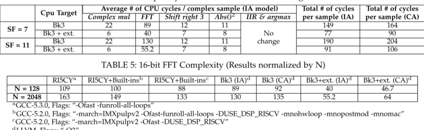
Average # of CPU cycles / complex sample (IA model) Total # of cycles Total # of cycles Cpu Target Complex mul FFT Shift right 3 Abs()2 IIR & argmax per sample (IA) per sample (CA)
Bk3 22 89 12 11 149 164 SF = 7 Bk3 + ext. 6 40 7 8 No 77 90 Bk3 22 130 12 11 change 190 204 SF = 11 Bk3 + ext. 6 55.2 7 8 91 106
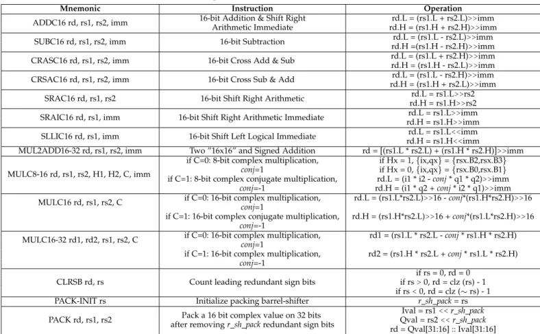
TABLE 5: 16-bit FFT Complexity (Results normalized by N)
RI5CYa RI5CY+Built-insb RI5CY+Built-insc Bk3 (IA)d Bk3 (CA)d Bk3+ext. (IA)d Bk3+ext. (CA)d
N = 128 109 100 88 89 92 40 46.7
N = 2048 163 149 133 130 135 55.2 64
aGCC-5.3.0, Flags: “-Ofast -funroll-all-loops”
bGCC-5.2.0, Flags: “-march=IMXpulpv2 -Ofast-funroll-all-loops -DUSE DSP RISCV -mnohwloop -mnopostmod -mnomac” cGCC-5.2.0, Flags: “-march=IMXpulpv2 -Ofast -DUSE DSP RISCV”
dLLVM, Flags: “-O3”
FFT employed in this algorithm, Table 5 shows a speedup of 49% and 53% for SF = 7 and SF = 11, respectively. Here, the “MULC16”, “ADDC16”, “SUBC16”, “CRASC16”, “CRSAC16”, and “SLLC16” instructions are used. We com-pare these results with those obtained using the same FFT algorithm but optimized to use the 16-bit SIMD options offered by the RI5CY processor [35]. Since the compiler is not the same, we also include results for the base RISC-V design. Table 5 shows an improvement of approximately 9%. These results can be improved to approximately 19% by enabling all of RI5CY’s hardware extensions (hardware loop, post increment, “MAC” instruction) but still remain more than a factor of 2 below our results. These results confirm our previous results in [9] which showed that the hardware extensions proposed in [28] are of limited interest for our application.
The speedup for the CORDIC 10-iteration kernel ap-plied on 16-bit complex data reaches 30% thanks to the “CRASC16”, “CRSAC16” and “SRAC16” instructions (Ta-ble 6). Next, the performance improvement of both the “CLRSB” and “PACK” instructions are studied indepen-dently in order to evaluate each instruction versus an equiv-alent efficient software implementation. The values reported in Table 7 correspond to the number of cycles required to execute a single iteration of each of the FOR loops defined in Figure 6. In particular, we observe the high efficiency (67% improvement) of the “CLRSB” instruction. These two in-structions are employed in the final LoRa demodulation test bench along with the “MULC16-32” instructions, leading to complexity improvements of 51% for SF = 7 and 52% for SF = 11 (Table 8). In all of these results, we observe that IA and CA model results are closely matched, validating the IA model-based instruction set exploration approach.
TABLE 6: Complexity of 16-bit CORDIC algorithm
Bk3 (IA)a Bk3 + ext. (IA)a Bk3 (CA)a Bk3 + ext. (CA)a
92 61 (-34%) 100 70 (-30%)
aLLVM, Flags: “-O3”
TABLE 7
Performance improvements of AGC instructions
Bk3 Bk3 + ext. Bk3 Bk3 + ext. (IA)a (IA)a (CA)a (CA)a
CLRSB 26 8 (-69%) 31 10 (-68%) PACK 12 8 (-33%) 13 9 (-31%)
aLLVM, Flags: “-O3”
6.5 IoT protocol results
Thanks to the above test bench complexity evaluations, we can now extrapolate the power consumption of the ex-tended core running these algorithms for specific IoT proto-cols. For each protocol, given the sampling rate of the input complex baseband signal, we first find the minimum core frequency required to process the samples in real time. Next, using power simulation results (including both dynamic and leakage power) obtained at different working frequen-cies for our proposed design synthesized with a sign-off frequency of 200 MHz, we extrapolate a linear power versus frequency model of the extended core for the algorithms in the test benches presented in Sections 5.1 and 5.2. These models are used to estimate the actual power consumption of each IoT protocol running at the corresponding minimum core frequency. Note that the power results reported below do not include the further energy savings that could be obtained using dynamic voltage scaling (DVS) allowed by the reduction of required CPU clock.
6.5.1 Bluetooth LE
The Bluetooth Low Energy (LE) physical layer employs the GFSK modulation at a 1 Msymbols/s signaling rate. Assuming an oversampling ratio (OSR) of 2 leading to an input sampling rate of 2 Msamples/s and extracting the worse-case complexity of 55 cycles/sample from Table 3 (Bk3+ext. CA model), we find that a minimum clock frequency of 110 MHz is required. Using our power versus frequency model, this results in a peak power consumption of 380 µW during the start-of-frame (SFD) phase of the frame detection algorithm. For comparison, in [24], a peak power of 1.372 mW is obtained for a similar Bluetooth LE work-load executed on a custom DSP processor in 28nm CMOS and using aggressive voltage scaling (0.45 V). Our work shows a more than three-fold improvement.
TABLE 8: Complexity of LoRa demodulation Algorithm
Total # of cycles Total # of cycles Cpu Target per sample (IA) per sample (CA)
Bk3 224 243
SF = 7
Bk3 + ext. 101 120 (-51%)
Bk3 264 284
12
6.5.2 LoRa preamble detection, BW = 125 kHz
A LoRa modulated signal can occupy a different wireless channel bandwidth depending on the spectrum availability of the country in which the system is deployed. In Europe and China, the most frequently employed bandwidth is 125 kHz. Assuming a minimum sampling rate receiver, the input sampling rate is thus 125 ksamples/s. From Table 4, we find that 90 and 106 cycles are required to process samples at SF = 7 and SF = 11, respectively. This leads to a minimum clock frequency of, respectively, 11.2 and 13.2 MHz. Using the extended core linear power model, this results in 110 µW and 116 µW, respectively.
6.5.3 LoRa preamble detection, BW = 500 kHz
In countries where larger ISM bands are available, such as in the USA, LoRa can be deployed on bandwidths up to 500 kHz, leading to greater bit-rates. Assuming a minimum sampling rate receiver, the input sampling rate is thus 500 ksamples/s leading to a minimum clock frequency for preamble detection of 45 and 53 MHz at SF = 7 and SF = 11, respectively. Using the extended core linear power model, this results in 203 µW and 225 µW, respectively.
Finally, we observe that, while the power consumption estimations above remain conservative seeing the addi-tional power savings that could be achieved in a solu-tion implementing dynamic voltage scaling, the numbers reported all remain compatible with our initial ultra-low power transceiver design goal. This is true even for com-putationally intense protocols such as maximum bandwidth LoRa preamble detection. Most importantly, in addition to allowing a considerable reduction of clock frequency and therefore of instantaneous power consumption, thanks to the important reduction of cycle count, the proposed ISA extension also allows a significant reduction in energy con-sumption.
C
ONCLUSIONIn this work, we present an instruction-set extension to the open-source RISC-V ISA which focuses on the acceleration of complex arithmetic used in physical-layer protocols of IoT communication schemes. To guarantee ultra-low power performance, instructions are designed to come at a near-zero power cost while reducing cycle count by more than 50% in complex arithmetic-intensive algorithms. The corre-sponding reduction in clock frequency results in substantial energy savings confirmed by post-synthesis power simula-tions of the extended core. By proving the feasibility of ultra-low power performance even for computationally intense protocols such as maximum bandwidth LoRa preamble detection and Bluetooth Low Energy, this work paves the way to making ultra-low power software-defined radio a reality.
A
CKNOWLEDGMENTSCarolynn and Hela thank Vincent Morice (now with STMi-croelectronics) for his contribution to embedded software design for LoRa, Franc¸ois Dehmas of CEA, LETI for his ex-pertise in DBB protocols, all of the members of the LFIM and LSTA laboratories of CEA, LIST for their infinite patience in
answering our questions concerning microarchitectures, and Zdenˇek Pˇrikryl and Jerry Ardizzone of Codasip for making this research possible.
R
EFERENCES[1] R. G. Machado and A. M. Wyglinski, “Software-Defined Radio: Bridging the Analog–Digital Divide,” Proceedings of the IEEE, vol. 103, no. 3, pp. 409–423, 2015.
[2] A. Kamaleldin, S. Hosny, K. Mohamed, M. Gamal, A. Hussien, E. Elnader, A. Shalash, A. M. Obeid, Y. Ismail, and H. Mostafa, “A reconfigurable hardware platform implementation for software defined radio using dynamic partial reconfiguration on Xilinx Zynq FPGA,” in 2017 IEEE 60th International Midwest Symposium on Circuits and Systems (MWSCAS), 2017, pp. 1540–1543.
[3] D. C. Dinis, R. Ma, S. Shinjo, K. Yamanaka, K. H. Teo, P. V. Orlik, A. S. R. Oliveira, and J. Vieira, “A Real-Time Architecture for Agile and FPGA-Based Concurrent Triple-Band All-Digital RF Transmis-sion,” IEEE Transactions on Microwave Theory and Techniques, vol. 66, no. 11, pp. 4955–4966, 2018.
[4] M. R. Maheshwarappa, M. D. J. Bowyer, and C. P. Bridges, “Improvements in CPU FPGA Performance for Small Satellite SDR Applications,” IEEE Transactions on Aerospace and Electronic Systems, vol. 53, no. 1, pp. 310–322, 2017.
[5] R. Nivin, J. S. Rani, and P. Vidhya, “Design and hardware imple-mentation of reconfigurable nano satellite communication system using FPGA based SDR for FM/FSK demodulation and BPSK modulation,” in 2016 International Conference on Communication Systems and Networks (ComNet), 2016, pp. 1–6.
[6] L. Ouvry, D. Lachartre, C. Bernier, F. Lepin, F. Dehmas, and V. Des-landes, “An Ultra-Low-Power 4.7mA-Rx 22.4mA-Tx Transceiver Circuit in 65-nm CMOS for M2M Satellite Communications,” IEEE Transactions on Circuits and Systems II: Express Briefs, vol. 65, no. 5, pp. 592–596, 2018.
[7] C. Gavril˘a, C. Kertesz, M. Alexandru, and V. Popescu, “Reconfig-urable IoT Gateway Based on a SDR Platform,” in 2018 Interna-tional Conference on Communications (COMM), 2018, pp. 345–348. [8] E. A. Waterman and K. Asanovic, Eds., The RISC-V Instruction Set
Manual, Volume I: User-Level ISA, Document Version 2.2. RISC-V Foundation, May 2017.
[9] H. Belhadj Amor and C. Bernier, “Software-Hardware Co-Design of Multi-Standard Digital Baseband Processor for IoT,” in 2019 Design, Automation Test in Europe Conference Exhibition (DATE), March 2019, pp. 646–649.
[10] D. S. Truesdell, J. Breiholz, S. Kamineni, N. Liu, A. Magyar, and B. H. Calhoun, “A 6–140-nW 11 Hz–8.2-kHz DVFS RISC-V Microprocessor Using Scalable Dynamic Leakage-Suppression Logic,” IEEE Solid-State Circuits Letters, vol. 2, no. 8, pp. 57–60, 2019.
[11] P. Davide Schiavone, F. Conti, D. Rossi, M. Gautschi, A. Pullini, E. Flamand, and L. Benini, “Slow and steady wins the race? A comparison of ultra-low-power RISC-V cores for Internet-of-Things applications,” in 2017 27th International Symposium on Power and Timing Modeling, Optimization and Simulation (PATMOS), 2017, pp. 1–8.
[12] R. Uytterhoeven and W. Dehaene, “A sub 10 pJ/Cycle Over a 2 to 200 MHz Performance Range RISC- V Microprocessor in 28 nm FDSOI,” in ESSCIRC 2018 - IEEE 44th European Solid State Circuits Conference (ESSCIRC), 2018, pp. 236–239.
[13] E. Flamand, D. Rossi, F. Conti, I. Loi, A. Pullini, F. Rotenberg, and L. Benini, “GAP-8: A RISC-V SoC for AI at the Edge of the IoT,” in 2018 IEEE 29th International Conference on Application-specific Systems, Architectures and Processors (ASAP), 2018, pp. 1–4. [14] Texas Instruments. CC1310 Datasheet. [Aug. 15, 2020]. [Online].
Available: https://www.ti.com/product/CC1310
[15] A. Pullini, F. Conti, D. Rossi, I. Loi, M. Gautschi, and L. Benini, “A Heterogeneous Multicore System on Chip for Energy Efficient Brain Inspired Computing,” IEEE Transactions on Circuits and Sys-tems II: Express Briefs, vol. 65, no. 8, pp. 1094–1098, 2018.
[16] Y. Pu, C. Shi, G. Samson, D. Park, K. Easton, R. Beraha, A. Newham, M. Lin, V. Rangan, K. Chatha, D. Butterfield, and R. Attar, “A 9-mm2 Ultra-Low-Power Highly Integrated 28-nm CMOS SoC for Internet of Things,” IEEE Journal of Solid-State Circuits, vol. 53, no. 3, pp. 936–948, 2018.
![Fig. 1: Simplified architecture of software-defined RF re- re-ceiver (reproduced from [9])](https://thumb-eu.123doks.com/thumbv2/123doknet/12899005.371271/3.918.73.450.62.172/fig-simplified-architecture-software-defined-rf-ceiver-reproduced.webp)

![TABLE 2: Comparison of different core architectures Processor core [39] ab Bk3 c Bk3 + ext](https://thumb-eu.123doks.com/thumbv2/123doknet/12899005.371271/11.918.80.449.69.225/table-comparison-different-core-architectures-processor-core-bk.webp)