45nm Direct Battery DC-DC Converter for Mobile
MASSACHUSETTS INSTIT E
Applications
OF TECHNOLOGYby
JUL 12 2010
Saurav Bandyopadhyay
LIBRARIES
B.Tech Indian Institute of Technology, Kharagpur (2008)
M.Tech Indian Institute of Technology, Kharagpur (2008)
Submitted to the Department of Electrical Engineering and Computer
Science
in partial fulfillment of the requirements for the degree of
Master of Science in Electrical Engineering and Computer Science
at the
ARCHIVES
MASSACHUSETTS INSTITUTE OF TECHNOLOGY
June 2010
@
Massachusetts Institute of Technology 2010. All rights reserved.
A uthor ...
...
Department of Electrical Engineering and Computer Science
May 21, 2010
Certified by
... ..
.
...
Anantha P. Chandrakasan
Joseph F. and Nancy P. Keithley Professor of Electrical Engineering
Thesis Supervisor
A ccepted by ...
...
Terry P. Orlando
Chairman, Department Committee on Graduate Theses
45nm Direct Battery DC-DC Converter for Mobile
Applications
by
Saurav Bandyopadhyay
Submitted to the Department of Electrical Engineering and Computer Science on May 21, 2010, in partial fulfillment of the
requirements for the degree of
Master of Science in Electrical Engineering and Computer Science
Abstract
Portable devices use Lithium-ion batteries as the energy source due to their high en-ergy density, long cycle life and low memory effects. With the aggressive downscaling of CMOS, it is becoming increasingly difficult to efficiently interface the low voltage, low power digital baseband and DSP of the mobile phone with the battery which maybe at voltages as high as 4.2V. This is efficiently done by a DC-DC converter which is a separate IC designed on an older generation process capable of handling high voltages. However, this requires an extra IC, thereby increasing the overall sys-tem cost. Here, a buck converter is demonstrated on a standard 45nm digital CMOS process which can be integrated with the 45nm digital core on the same die. This converter is capable of handling high battery voltages (2.8V to 4.2V) and delivers a regulated low voltage (0.5V to 1.1V) to the digital core. The converter can supply 20pA to 100mA of load current. The peak efficiency of the converter is 87% for 73mW output at 4.2V supply and for the ultra low power levels, efficiency of 75% is obtained for a 20tW load at 3V. Both pulse width modulation (PWM) and pulse frequency modulation (PFM) modes of control are used. A new digital pulse width modulator (DPWM) architecture is presented which provides 75% area savings over the conventional delay line and counter based architecture with comparable power consumption. The buck converter also requires Switched Capacitor (SC) DC-DC Converters to generate stacking regulators and regulator for the control circuitry. On the whole, the complete system integrates the Power Management Unit with the core for a single chip radio in 45nm.
Thesis Supervisor: Anantha P. Chandrakasan
Acknowledgments
I would first like to thank my parents and my grandfather for believing in me even when I did not. No words are enough to express their selfless love, affection and support. Over the years they have helped me through all the tough times. I cannot thank them enough. I would also like to thank my advisor Prof. Anantha Chan-drakasan for being more than just a mentor. He has been an ideal role model for all of us. I would also like to thank Dr. Yogesh Rarnadass who has taught me ev-erything I know about Power Converters! Every discussion with him is stimulating, even the non technical ones like cursing the Indian cricket team whenever they lost. Without his help I would not have been able to tape-out on time. Dr. Alice Wang at Texas Instruments. She always had the time and patience to answer all my questions regarding the process. It was because of her support (and DRC waivers!!) that my design went for fabrication. Margaret, our administrative assistant, for doing so much for all of us that we don't even realize. Also to the students of ananthagroup, who have made our lab a wonderful environment to work in. Last but not the least, I am grateful to my roommates Rahul Rithe and Rishabh Singh for bearing with me for the last two years.
Contents
1 Introduction
1.1 Motivations for Direct Battery DC-DC Converter . . . . 1.2 Background Work .
1.3 Thesis Organization... . . . .
2 System Architecture
2.1 Power Stage of Buck Converter 2.1.1 Power Transistor Sizing 2.1.2 Output Filter Design . . 2.1.3 Level Shifters . . . . 2.1.4 Gate Drivers . . . . 2.2 Switched Capacitor Converters
2.2.1 1.8V Switched Capacitor 2.2.2 Stacking Converters . 2.3 Control Architecture . . . . 2.3.1 PWM control . . . . 2.3.2 PFM control . . . . 2.3.3 DPWM architecture . . 2.3.4 Chapter Summary . . . 19 . . . . 19 . . . . 20 . . . . 23 . . . . 25 . . . . 27 . . . . 29 Converter.. . . . .. 29 . . . . 32 . . . . 40 . . . . 40 . . . . 4 3 . . . . 4 6 3 Measurement Results
3.1 Die Micrograph and Board . . . . 3.2 Efficiency Plots... . . . . . . . . ..
. . . . 1 5
53 53 54
3.3 Transient Response . . . . 56 3.4 Comparison of Measured Results . . . . 57
4 Conclusion and Future Work 61
4.1 Main Contributions.. . . . . . . . 61 4.2 Design Summary . . . . 62 4.3 Further Work . . . . 62
List of Figures
1-1 Discharge curve of Lithium Ion battery . . . . 1-2 Block Diagram of DC-DC converter with digital baseband/DSP
Block level architecture of Power Converter . . . . . Architecture of Power Converter... . . . . . . . . Optimal Width for minimum loss ...
Simulated losses in the power stage . . . . Conventional Level Shifter.... . . . . . . . Capacitive Coupled Level Shifter . . . . Simulation result of capacitive coupled level shifter from 0, 1.8V to VBAT-1.8V, VBAT -...
Gate Drive for PMOS in power stage . . . . Simulation showing the gate drive circuit output with are inverted and level shifted versions . . . . 1.8V SC with three gain settings. . . . . .. PFM loop of 1.8V SC . . . . Simulation of PFM loop of 1.8V SC . . . . Gate volatges of the power FETs . . . . VBAT-1.8V and VBAT-3.6V regulators.. . . . .. VBAT-1.8V and VBAT-3.6V regulators . . . . Strong ARM comparator . . . . 2-17 High Voltage tolerant Strong ARM comparator 2-18 High Voltage tolerant Strong ARM comparator
. . . . shifting the rails 2-1 2-2 2-3 2-4 2-5 2-6 2-7 2-8 2-9 2-10 2-11 2-12 2-13 2-14 2-15 2-16
.. . . .. .. . .
two inputs which
. . . . 28 . . . . 30 . . . . 31 . . . . 32 . . . . 33 . . . . 34 . . . . . 35 . . . . 36 . . . . 37 . . . . 38
2-19 Clock Gating Circuit for Stacking Regulators . . . . 39
2-20 Simulations of the clock gating circuit . . . . 40
2-21 Architecture of Control Circuitry.. . . . . . . . . 41
2-22 4 bit Flash ADC... . . . . . . . 42
2-23 PFM simulation.. . . . . . . . 44
2-24 Total Loss with optimal tp . . . . 45
2-25 Concept of Zero Current Switching . . . . 47
2-26 Delay line based DPWM architecture . . . . 48
2-27 DPWM architecture with sleep control . . . . 49
2-28 Capacitor voltage increasing linearly with time . . . . 51
2-29 Simulated waveforms showing the comparator current, sleep signal and the DPWM output to PMOS power FETs . . . . 52
3-1 Die Microphotograph... . . . . . . . . 53
3-2 Board with IC and off-chip components . . . . 54
3-3 Measured Efficiency of DC-DC Converter for various battery voltages 55 3-4 Breakup of Overall Power Loss . . . . 56
3-5 Load Transient from 1OOuA to 5mA.. . . . . . . . . 57
3-6 Load Transient from 5mA to 1OOuA . . . . 58
List of Tables
1.1 SIA technology direction . . . . 13
1.2 CMOS DC-DC buck converters . . . . 16
1.3 Previous Work with Design Targeted . . . . 17
2.1 DPWM techniques... . . . . . . . . 48
2.2 comparison of DPWM performance . . . . 50
3.1 Comparison of Measured Results . . . . 59
Chapter 1
Introduction
Hand-held portable electronics have significantly advanced in the last decade. Moore's law has enabled us to integrate more and more functionality on a chip. With each scaled generation, the number of transistors on a die has doubled, the gate oxide has scaled and the nominal voltage has reduced [1]. Table 1.1 shows the trend of scaling as predicted by the SIA road-map published in 1999. Although with scaling the gate capacitance reduced, the leakage increased due to the small channel lengths. With increased complexity, integration and functionality, the total power consumption has increased. Circuit designers have tried to alleviate the power problem by using tech-niques like Ultra Dynamic Voltage Scaling (U-DVS) [2], parallelism, power gating and clock gating [3]. U-DVS requires changing the supply to the digital circuit on the fly. In such cases it is essential to have a highly efficient DC-DC converter converting battery voltage to a lower voltage desired for U-DVS to be effective. Optimizations right at the power source would provide us with large energy savings and would help extend the lifetime of these devices [4].
Table 1.1: SIA technology direction
Case 1999 2002 2005 2008 2011 2014
Technology 0.18pm 0.13pm 0.10pm 70nm 50nm 35nm Nominal Supply Voltage 1.8V 1.5V 1.2V 0.9V 0.6V 0.6V
Gate Oxide Thickness 2.5nm 1.9nm 1.5nm 1.2nm 0.8nm 0.6nm Transistors/chip (million) 24 95 190 530 1500 4300
1.1
Motivations for Direct Battery DC-DC
Con-verter
With advances in battery technology, it has been shown that Lithium-ion batteries provide a high energy density and long cycle time [5] making them ideal candidates for portable applications. Fig 1-1 shows the discharge curve of a 2AH Lithium-ion battery. When fully charged, the battery has a voltage of 4.2V. When discharged to moderate levels, its voltage is close to 3.7V. Beyond this, the voltage drops steeply to below 3V. For any portable application, we need to ensure that it can work for voltages ranging from about 2.8V to 4.2V.
0 250 500 750 1000 1250 1500 1750
Discharge Capacity (mAh)
FULL
3/4
1/21/4
1/8
2000Figure 1-1: Discharge curve of Lithium Ion battery
Typically, the power management unit (PMU) is a set of ICs capable of handling high voltages supplying power to the low voltage low power ICs. The DC-DC convert-ers in the PMU are designed on an older generation process. Integrating the DC-DC converter with the digital baseband/DSP [6] on the same die would remove the cost
of an extra IC , the cost of integrating it on the board and would also reduce the board footprint. The nominal supply for 45nm node is 1.1V and for circuits employ-ing U-DVS, voltages as low as 0.5V may be used. The key challenge lies in designemploy-ing a converter at the 45nm node that can handle the high battery voltage.
The process used in this work provides some high voltage devices but even then stacking multiple high voltage devices is necessary. The main aim is to have a com-plete efficient PMU at 45nm which can handle the high battery voltage. The high voltage devices with stacking make this extremely difficult to achieve. The system block diagram is shown in Fig 1-2.
Lithium Ion battery (3V - 5.5V) F --- I
Cn rtrseband/
DSP of
obile
Full integration for single
chip solution at 45nm
Figure 1-2: Block Diagram of DC-DC converter with digital baseband/DSP
1.2
Background Work
Integrated CMOS DC-DC converters have enabled us to have power conversion on-chip instead of the discrete component solution. It must be noted that CMOS buck converters usually have all circuits integrated except the off-chip LC filter. Table 1.2 summarizes a few of such converters with their corresponding contributions and performance.
As seen in Table 1.2, the CMOS DC-DC converters are mainly used for U-DVS systems. It is preferred that the converters be integrated with the load circuit (DSP
[7] or microprocessor [8]). All the converters cited here except [9] are designed within the allowed voltage limits of the process. This makes achieving high efficiencies a lot simpler than this work. Since we are going beyond the limit of the process, additional control circuitry and stacking is required that limits the overall efficiency. A high voltage DC-DC converter design on 40nm is presented in [10] but it is not an autonomous system as the control circuit is powered not using the main battery. Also, the design can handle only up to 3.3V unlike a direct battery converter.
Table 1.2: CMOS DC-DC buck converters Contributions
[4] Adaptive dead time control and zero voltage switching (ZVS) to minimize capacitive switching loss in power stage
[11] Digital PID controller for buck con-verters first reported with DPWM using a high speed clock and mul-tiplexer for creating pulses
[12] DPWM architecture with delay line and counter first reported
[7] Dynamic Voltage Scaling applied to a DSP with embedded DC-DC Con-verter
[8] Dynamic Voltage Scaling system with microprocessor embedded DC-DC Converter
[9] Dual Mode direct battery DC-DC converter with PWM and PFM modes of control and stacking in power stage
[10] High input voltage DC-DC con-verter with PWM mode only [13] Commercial direct battery design
from Texas Instruments with both PWM and PFM control modes [14] Dynamically changing the output
voltage to the minimum energy point voltage of a given circuit
Converter Performance 79% efficient at 750mW
1.2pm CMOS
load using
92.9% peak efficiency for 1.38W but using off-chip switches
peak efficiency 89% for 20mW out-put on 0.6pm CMOS
Total power savings of 30-50% with embedded DC-DC converter on 0.8pum 80% to 90% efficiency of DC-DC on 0.6pm CMOS 70% to 91% efficiency on 0.25pm CMOS >90% for 0.1 to 1W output at 40nm 49% to 65% efficiency for 90pW out-put and peak efficiency of 95% for 90mW output on a process that can handle high battery voltages
81% to 86% for 1pW to 10pW of load
[9] is direct battery DC-DC converter on 0.2 5pm CMOS having nominal supply Case
of 2.5V. The output power being delivered is 150pW to 0.6W. The design [13] is a commercially available IC. The process used for the design is not known but it can handle high voltages without any extra stacking in the power stage. However, no published work addresses the issues in direct battery power converters at ultra- low power levels (10's of pW) to medium power levels (0.1W) that maintain efficiency throughout this range in 45nm. Table 1.2 summarizes a comparison between the direct battery DC-DC converters cited and the targets of this design.
Table 1.3: Previous Work with Design Targeted
Case [9] [13] Target for this
work
Technology 0.25um process capable 45nm
of handling high voltages
Nominal Supply 2.5V
1.IV
Voltage
Battery Volatge 2.8V to 5.5V 2.7V to 6V 2.8V to 4.2V Output Power 150pW to 0.6W 90pW to 0.54W i0aW to 0.1W Load Current 100pA to 0.4A 50pA to 0.3A 101A to 0A Stacking in power Yes No as process al- Yes
stage lows high voltage
Peak Efficiency for 70% for 150pW 65% for 90,aW >80% for 101iW
ultra-low power
Overall Peak Effi- 91% for300mW 95% for 90mW >90% for 100mW ciency
As seen, this work targets much lower power as compared to previously published work. Also, since the latest Li-ion battery chargers have a control circuit preventing the battery from overcharging after 4.2V, there is no need for us to go upto 5.5V as in the designs in Table 1.3. Thus, the main aim of this work is to obviate the need of the extra IC like [9] and [13] and have the DC-DC conversion on the same die at the 45nm node.
1.3
Thesis Organization
This thesis presents a completely self-contained direct battery DC-DC converter at 45nm. Chapter I gives the main motivation behind the design and does a review of literature. As seen, a high voltage DC-DC converter is a challenging design at scaled
technologies like 45nm. With increased complexity due to stacking, in this design we also deal with a large dynamic range of load conditions. This makes achieving decent efficiencies for the whole range difficult. For light loads, leakage and conduction losses limit the efficiency. For heavy loads, the conduction losses in the power stage limits the efficiency. Chapter 2 discusses the design architecture and the circuit techniques used. Techniques like power gating and clock gating have been used in this work to achieve a highly efficient power converter. As shown, Chapter 3 presents measurement results of the design and makes comparisons with the designs cited before. This design is one of the widest output power range DC-DC converter. Chapter 4 concludes the thesis and provides future directions for this work.
Chapter 2
System Architecture
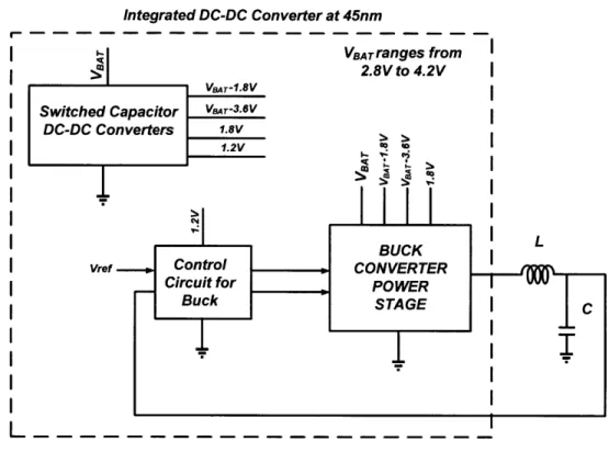
Power conversion is done by three types of DC-DC converters. The switching regu-lators (eg. buck, boost) provide a highly efficient solution but require an off-chip LC filter. Switched Capacitor (SC) converters on the other hand provide a completely on-chip solution but at the expense of efficiency. LDOs, which are not considered in this work, are the third type of power converters generally used. These are the least efficient among all the converters described.
Fig 2-1 shows the block level architecture of the design. The main converter used is a buck converter converting the high battery voltage to the desired low regulated voltage. The SC converters generate the intermediate stacking voltages (VBAT-1.8V and VBAT-3.6V) and voltages for control (1.8V and 1.2V). These are used by the
main buck converter for its power stage and control circuit making the system a fully integrated DC-DC converter at 45nm. The power stage and the SC converters use high voltage transistors but the control circuit shown uses the core 45nm devices.
2.1
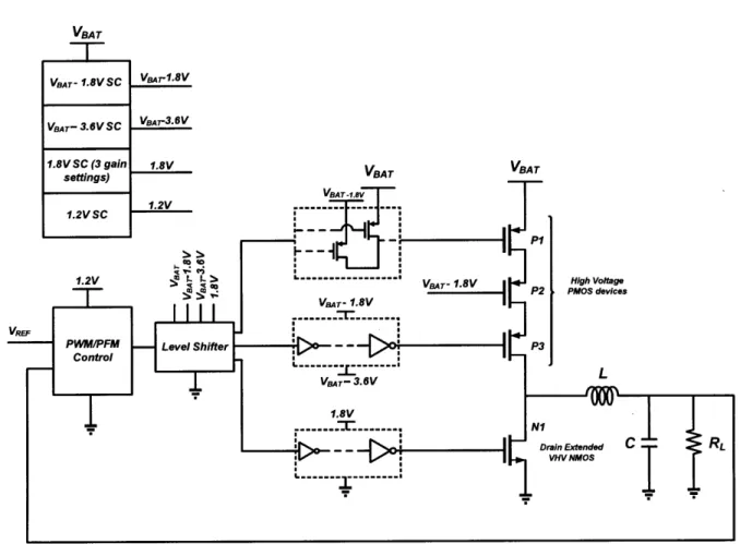
Power Stage of Buck Converter
The power stage of the buck converter consists of the power transistors, the gate drive circuits, level shifters and the output LC filter. From Fig 2-2, it can be seen that the power stage is asymmetric. Three high voltage PMOS transistors have been stacked and only one NMOS transistor is used. Each PMOS transistor can handle a
Integrated DC-DC Converter at 45nm
VBAT ranges from 2.8V to 4.2V
Switched Capacitor Var-3.6V
DC-DC Converters 1.8v
BUCKL
Vref Control CONVERTER
Circuit for POWER
Buck ST AGE
C
L
Figure 2-1: Block level architecture of Power Converter
certain VDS and VGS given by the process. Since we have to handle a battery voltage
greater than 3.6V, three devices have been stacked. On the NMOS side, the device used is a very high voltage drain extended device that can handle very high a VDS.
Stacking on the NMOS side using the high voltage transistors (similar to the PMOS high voltage devices used) is not preferred as this would require an extra deep n-well for isolation, thus increasing the cost of processing. In this design, the bulk of all the NMOS transistors have been tied to ground obviating the need for an extra mask. The NMOS transistor in the power stage has a VGS of 1.8V when it is on. The power for driving the gate of this transistor is supplied by the 1.8V SC converter.
2.1.1
Power Transistor Sizing
In the PWM mode, the loss in the power stage is dominated by the switching loss and the conduction loss. The switching loss is given by CVAD2fCLK, VDD being the higher
VBAT
VBAT- 1.8VSC VBAr1.8V
VBAT- 3.6V SC VBAI-3.6V
1.8VSC (3 gain 1.8V VBA VBAT
settings) T VBAT -1.6V 1.2V ... .... ... 1.2VSC P1 1.2V L- --- V -18 High Voltage
TBAT-
1.8V P2 PMOS devicesVaAr-
1.8V
VREF --- F- Level Shifter rP -CP3 __ L VATr- 3.6V 1.8V ...- - --- N1 -- Drain EtndedFigure 2-2: Architecture of Power Converter
rail for the gate drive circuit, C the total gate capacitance and fCLK, the switching
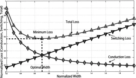
frequency of the converter. The conduction loss is given by IourR where IOUT is the dc current being delivered and R is the on resistance of the transistor. Here, the current ripple ridding over the dc current of IOUT is ignored for PWM. For a more detailed analysis, we need to consider the rms power loss, which depends also on the inductor in the output filter. As the gate capacitance is directly proportional to the transistor width, wider the transistor, more is the switching loss. On the other hand, the on resistance is inversely proportional to the transistor width. These opposing trends give a optimum width of a given load current. If we consider CzzkiW and R=k2/W, where ki and k2 are two process dependent constants, the total loss is
given by the following equation,
loss = k1WV3DfCLK + IOUTk2|W (2.1)
For a given IOUT, VDD and frequency, the optimum width is given by
Woptimum = (IuTk2)/(k1VDDfCLK) (2.2)
Fig 2-3 shows the optimal normalized width for minimum loss in the power stage. In this work, the transistor N1 has been sized optimally for 50mA load current. The sizing of the PMOS power transistors has been done to preserve the PFM efficiency at light loads which will be discussed later in this subsection.
t - -- - - - --2 - Tota Loss Minimum Loss - - -- Switching Loss .2 - - - Conduc on Loss Ue Optima llmidth* z'
Normalized Width
Figure 2-3: Optimal Width for minimum loss
The breakup of simulated power loss in the power stage is shown in Fig 2-4 for
62mW output power. As seen, a large fraction (61%) of the loss is due to the very
high voltage drain extended NMOS. It must be noted that the switching loss in the
NMOS is mainly dominated by the CV2/CLK loss due to charging up the drain to
gate capacitor when PMOS power transistors are on and NMOS power transistor is off. As the drain voltage has to go up all the way up to VBAT, it is this loss that dominates the overall switching loss rather than just the loss in the NMOS gate drive circuit to switch on the NMOS power transistor.
1.12mW PMOS Conduction Loss
0.12mW Drain Capacitance Switching Loss 0.128mW Loss in Inductor ESR
0.13mW Loss in parasitic diodes 1.28mW NMOS Conduction Loss
1.41mW NMOS Switching Loss
0.21mW PMOS Switching Loss
Figure 2-4: Simulated losses in the power stage
The PMOS transistors are intentionally not sized optimally for 50mA load in PWM, as the conduction loss is much more than switching loss. For loads less than 100pA, the leakage through the PMOS transistors starts to hurt the efficiency. To ensure that efficiency is preserved even at light loads, the transistors in the stack were sized such that the leakage was less than 80nA. This translates to <4% drop in
efficiency at 10pW output load in PFM.
2.1.2
Output Filter Design
The inductor and capacitor values have been selected so that the current ripple and voltage ripple are within acceptable limits of design. Also, loop stability needs to be considered when the controller is designed for the PWM mode. The current ripple in the inductor current is given by the following expression.
Iripple = VBAT(1 - D)D/(2Lf)
L is the inductance, D is the duty cycle and f is the switching frequency of the converter. Iripple is maximum when VBAT is 4.2V and VOUT is 1.2V. For a switching frequency of 2MHz and inductor of 10pH, current ripple is 23mA. This translates to 0.8mW rms conduction loss, 33% of the total conduction loss given by Fig 2-4.
The voltage ripple is given by the following expression. For a 2p-F capacitor, the voltage ripple is less than 1mV. As the output filter ripple is extremely small, the other sources of ripple, e.g ripple in SC effecting the switching of the transistors, dithering in PWM dominate the overall voltage ripple.
Vrippie = Irippie(8Cf
)
(2.4) VBAT VBAT VBAT-1.8V 1.8V0
L
Y--VBAT§LF
VBAT-1.8V .8VVFigure 2-5: Conventional Level Shifter
2.1.3
Level Shifters
The gate driver of the PMOS power transistor P1 as shown in Fig 2-2 needs to have
VBAT and VBAT-1.8V as the two rails between which the gate voltage will be switching. For P3, the rails required are VBAT-1.8V and VBAT-3.6V. Level shifters are required to shift the rails so that the PMOS power FETs can be effectively switched. For a signal between OV and 1.8V, the traditional level shifter used to shift the rails to
VBAT-1.8V and VBAT is shown in Fig 2-5. Its a DCVSL type of structure but since
the level shifter signal cannot go rail to rail, that is from OV to VBAT, we require
extra PMOS devices to prevent the voltage from going all the way down to OV. The problem with this circuit is that it is inherently slow due to its ratioed nature and does not scale well with the battery voltage.
VBAT
VBAT-1.8V VBAT-1.8V
VBAT VBAT
VBAT-1.8V VBAT-1.8V
1.8V
Figure 2-6: Capacitive Coupled Level Shifter
In this work, a capacitively coupled level shifter is designed. This is inherently low power and scales well with the battery voltage. However, we need to ensure that this circuit works even at low frequencies. Leakage might cause the level shifted output to change if the input remains constant for a long period, hence making this a dynamic
circuit. The circuit diagram is shown in Fig 2-6. Extra diodes are used to ensure that the output always remains between VBAT and VBAT-1.8V. In this design, we have two such level shifters, one to shift the supply rails to VBAT-1.8V and VBAT and the other for the rails VBAT-3.6V and VBAT-1.8V.
Level Shlfter Simulaton
200 300 400 s5 r 60I time(ns)
700 800 900 1000
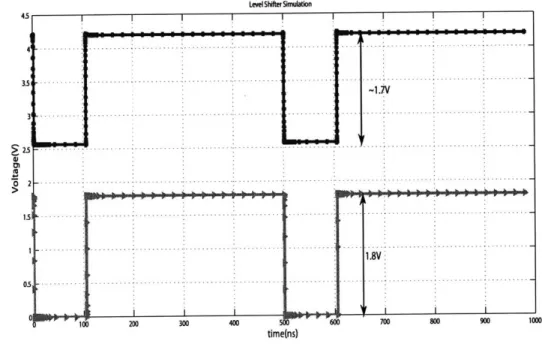
Figure 2-7: Simulation result of capacitive coupled level shifter shifting the rails from 0, 1.8V to VBAT-1-8V, VBAT
Fig 2-7 shows the simulation result of the capacitive coupled level shifter in the PWM mode. The bottom waveform is a 2MHz signal that goes from OV to 1.8V. This is the input to the level shifter. The output is the top waveform swinging from 2.5V to 4.2V. It must be noted that the swing is slightly reduced at the output due to charge sharing between the coupling capacitor and the associated parasitic capacitors the the output node. The coupling capacitors used in this design were metal to metal capacitors so that the associated parasitic capacitors are minimized. This swing can be restored by a subsequent DCVSL inverter stage or a pass transistor gate drive discussed later.
ill]
..
7
...
L
...
ij...
...
.... ... .... ... ... .. ... ... .. ... .. ..... . . .. . . .. . . .. . . .. .. . .. .. . .. I.. .. .. .. .. . . .. . ICE 00114111111101111101 § - I I2.1.4
Gate Drivers
In order to drive the power transistors, we have to design gate drivers. For the NMOS in the power stage, the driver is a string of inverters, each subsequent inverter scaled so that the final inverter has enough strength to drive the power transistor. For the PMOS, P3, we can use a string of inverters. However, for the PMOS, P1, connected
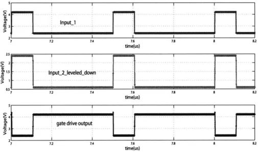
directly to the battery, an inverter structure cannot be used. This is because the NMOS transistor in the inverter would be having a VBAT at its gate. For such a case a gate drive circuit has been proposed that uses pass transistors in manner that avoids any NMOS transistor from getting a very high voltage at the gate. The circuit is shown in Fig 2-8. VBAT VBAT VBAT - 1.8V I Input_1 VBAT-1.8V VBAT-1.8V P2 N1 VBAT- 1.8V VBAT- 3.6V Input_2_leveleddown VBAT VBAT- 1.8V Output
Figure 2-8: Gate Drive for PMOS in power stage
Essentially, this circuit performs an inversion operation without any NMOS with
VBAT at its gate. P1 and P2 are the main drivers for the next stage. This requires two inputs which are level shifted and inverted versions of each other as shown in Fig
2-8. P1 is on when its gate voltage is VBAT-1.8V. During this time, the gate voltage of P2 has to be VBAT to prevent any conducting path from VBAT to VBAT-1-8V through P2. P3 and P4 ensure this. Meanwhile, N1 is off. Hence, the output of the circuit is VBAT. For the case when input to P1 is VBAT and to N1 is VBAT-1.8V, the gate of P2 gets VBAT-3.6V. This ensures P2 is on and P1 is off. Hence, the output is VBAT-1.8V.
Thus, we can see that an inversion operation has been performed by just PMOS pass transistors and one NMOS which does not have to face VBAT at its gate. Cascading multiple such stages and scaling them helps us to have a PMOS gate driver. The simulation result of this circuit is shown in Fig 2-9.
81 n ul . . . ... ... . Input_1 7 7 7.4 7.6 7. 8 8.2 time(us) 2.5 ,2
...
...
h i
0_ nput2jeveed down... .... ... .. 0.s1 7 7 7.4 7.6 7.8 8 L2 time(us) sgate drive output
> L
7 7.2 7. 7.6 7. 8 8.2
time(us)
Figure 2-9: Simulation showing the gate drive circuit output with two inputs which are inverted and level shifted versions
Input_1 shows the level shifted input from the previous gate drive stage. This signal goes to the gates of P1 and P4. Input_2_leveled-down is the second input that is the level shifted and inverted version of Input_1 and goes to the gate of N1. Since, Input_2_leveled-down swings between VBAT-1.8V and VBAT- 3.6V, it can be generated
using inverters. In this implementation, the circuit generating Input_2_leveled-down and the gate driver for P3 of Fig 2-2 is shared.
will not effect the functionality. This becomes important when the input is directly from a level shifter instead from the similar predecessor stage. As it was pointed out in a previous subsection, the swing may be slightly reduced due to charge sharing at the level shifter output node. This is only going to reduce the gate overdrive of P1 and P4 in Fig 2-8. This will make the signal transitions slower. By sizing the transistors properly, this effect can be reduced.
2.2
Switched Capacitor Converters
Since the goal of this work is to have a completely integrated converter, all the internal control and regulator circuits need to be powered by the battery which has a voltage between 2.8V to 4.2V. This includes the low voltage control circuit of the buck converter, and the extra regulators for the gate drives and the stack in power stage. A 1.8V Switched Capacitor converter has been designed that gets power directly from the battery and supplies power to all the control and other regulator circuits. As shown in Fig 2-2, there are four SC regulators in this design. VBAT-1.8V and VBAT-3.6V are for the PMOS stack in the power stage. 1.8V SC is used by these stacking regulators and their control to generate the corresponding voltages. The fourth SC is for generating 1.2V for the buck control circuit from the 1.8V SC. Thus, it can be seen that the 1.8V SC is the main converter driving all the other converters in the system.
2.2.1
1.8V Switched Capacitor Converter
Fig 2-10 shows the switch implementation of the 1.8V SC [15]. It also has the sim-plistic picture of the capacitor orientations at each switching phase. As the battery voltage can vary between 4.2V to 2.8V, we require three gain settings (3 switch con-figurations) for the SC converter. Reconfigurable switches are used to switch between gain settings. The 1by2 gain setting is used when the battery is fully charged to 4.2V. Once it discharges to 4V, 2by3 gain setting is used. For voltages below 3V, 1byl gain setting is used.
VBA T VL VL VBAT c VL VL VL 20C VL IC
1by2 Gain setting 2by3 Gain setting 1byl Gain setting
Figure 2-10: 1.8V SC with three gain settings
Considering 1by2 gain setting, the total output current delivered to the output is given by the following expression
IOUT = 4C(VBAT - 2VL)f (2.5)
where VL is the output voltage of the SC converter, f is the switching frequency and 2C is the total charge transfer capacitance. It must be noted that this equation assumes that the load capacitor is large enough to ignore the ripple. Therefore, the output power being delivered is
POUT = 4C(VBAT - 2VL)VLf (2.6)
In order to keep the charge transfer capacitors relatively small (within 50pF), the frequency of the SC circuits is 4MHz as compared to the system (buck converter switching) frequency of 2MHz in the PWM mode. In the PFM mode, since the current requirement of all the circuits is less, 1MHz suffices for both SC and the buck converter. The total charge transfer capacitance in the 1by2 gain setting is 45pF. Thus, by using power delivery equation from above, the SC converter can supply
VBAT 2 202 VBAT - VL 2C E-VL 2C VBAT
2C
2c
VLa maximum output power of 300pW, although the NMOS gate drive circuit when the buck converter is operating in the PWM mode consumes only 150IW. This extra margin is kept to ensure that the instantaneous droops in voltage due to the switching activity in the gate drive circuit is minimized. These sudden droops lower the gate overdrive of the NMOS power transistor increasing its on resistance. For the charge transfer capacitors in the SC, metal to metal capacitors have been used. Unlike the gate oxide caps, these can withstand a higher voltage across them. Since the charge transfer capacitors have to transfer the charge from the battery to the load in phasel, they will have a voltage across them that the gate oxide capacitors cannot handle. For a completely on-chip solution, the load capacitors of the SC converters are implemented by using gate oxide capacitors. These capacitors have been sized such that both leakage (<1OnA) and voltage droops are kept within acceptable limits of design.
Non ileveI shifted Switches with Regulated
Overlapping Level Charge Transfer 1.8V
Vref Clock 2 Shifters 21evelshifted Capacitors Generation
clk
I
Figure 2-11: PFM loop of 1.8V SC
The voltage regulation in the SC converter is done by a PFM loop. This consists of a comparator that triggers when the voltage falls below 1.8V. This sends a signal to the switches of the SC to change phase and hence transfer the stored charge to the load. Fig.2-11 shows the PFM loop details. A clock non-overlapping circuit is used to prevent any short circuit losses when phases change.
For the 1.8V SC, signals to most of the switches have to be level shifted. The level shifters used are the same capacitive coupled level shifters discussed in the previous
section. For the 1.2V
SC,
the architecture remains the same but no level shifters are used. The simulation results of the 1.8V SC are shown in Fig 2-12 with the level shifted version of#1_bar
and $2. The SC in this simulation supplies 90pW output power. 2.5 57 58 59 60 61 62 63 time(ps) 2.*2 -1 . 57 58 59 60 61 62 63 time(ps) 1.9 1.8V regulated I 1.9 0'12 .. . . .. . . . ... 1 .75 I 57 58 59 60 61 62 63 time(ps)Figure 2-12: Simulation of PFM ioop of 1.8V SC
2.2.2
Stacking Converters
There are two stacking converters used in this design. These are battery voltage scalable and provide regulated VBAT-1-8V and VBAT-3.6V. From Fig 2-2, the PMOS
stack in the power stage requires intermediate voltages to enable proper switching. Fig 2-13 shows the timing diagram of the gate signals. For 4.2V battery voltage, the gate voltage of P1 swings from 4.2V to 2.4V (VBAT-1-8V). The gate of P2 is held constant at 2.4V and the gate of P3 gets a signal which is the inverted version of the signal at gate of P1 but swings from 2.4V to 0.6V(VATr-3.6V). Therefore, for proper operation of the buck converter, the voltages VBAT-1.8V and VATr-3.6V should be
well regulated. By design, both these regulators are required to sink in current unlike the 1.8V SC which sources current. Even though the principle of operation is similar to an LDO or a lbyl gain setting SC converter, its design is slightly different.
~~~F..
... ...Gate voltage of P 4.2Vse~
3 . . ... .. .. ... ..to 24V voltage swing .. .. ..1.
... ... ... > 89.8 90 90.2 90A 90.6 90.8 91 91.2 time(ps)-J Gate voltage of P2 2.4V stead
002
> 892 90 902 90.4 90.6 908 91 91.2
time(ps)
2 - Gate voltageof P3148VtoO6V . ...
- voltage swing
00
> 898 90 902 90.4 90.6 90.8 91 912
time(pas)
.Figu r Gate voltage of NI 18VtoOV .
A i0 voltage swing ...
>8918 90 902 90.4 90.6 90.8 91 912
time(jis)
ist e hDrain voltageof N1/P3 4 aVVto.OVi
be
votage swing
dha
> 9890 902 90A eits90A 908 91 912
Figure 2-13: Gate volatges of the power FETs
Architecture of Stacking Regulators
Fig.2-14 shows the circuits for VBAT-1.8V and VBAT-3.6V regulators. The main aim
is to keep the voltage close to VBAT-1.8V and VBAT-3.6V. Since, the converter has to
be scalable with battery, the references designed for this converter have been made sliding. Stacking three diodes gives us a drop of 1.8V from the battery voltage. Another 3 diodes would give us another reference which is VBAT-3.6V. Hence, the
sliding diode reference provides the scalability feature required by the stack in order to operate effectively from 4.2V to 2.8V. The converter control is PFM. When the voltage is above the reference, the comparator triggers a switch that provides a path
to ground for the charge on the VBAT-1.8V load capacitor. Every time the comparator is triggered, a 4ns pulse is used to control the switch so that the voltage does not go all the way to ground. Since the NMOS transistor used in the 4ns delay is the same transistor that is used in the switch to discharge the capacitor, there is automatic process tracking in case there are variations.
VBA T VBA T VBA T -1.8V < Average Current into s1 C the circuit Strong ARM Latch clk VBAT -3.6V ' Average Current into .. the circuit Strong ARM
Latch
clkFigure 2-14: VBAT-1.8V and VBAT-3.6V regulators
For battery voltage of 3.6V, the sliding reference for VBAT-3.6V goes to almost OV. The regulator in this case tries to regulate the voltage to the reference, which is close to OV. For battery voltages below 3.6V, the regulator still maintains OV. However, now the PMOS power transistor P3 does not get an overdrive of 1.8V. Due to reduced overdrive, on resistance increases which affects the efficiency.
reference voltage regulated voltage comparator output 1 I II 82 83 84 85 86 8j time(ps)
Figure 2-15: VBAT-1.8V and VBAT-3.6V regulators
Fig 2-15 shows the simulation result of the VBAT-1.8V regulator. The input current is a 10pLA de current. The comparator triggers when the output goes above the reference. The comparator output is shown along with the reference and regulated voltage.
High Voltage tolerant Strong ARM comparator
All the comparators used in the design are similar to the Strong ARM register [16]. However, for the VBAT-1.8V regulator, the comparator needs to be slightly modified from the conventional Strong ARM design. For the circuit shown in Fig 2-16, a PMOS transistor is used with a sense amplifier in the comparator. In this circuit, the output nodes VoUT+ and VOUT of the comparator will be swinging between 0 and VBAT. Since, these nodes are connected to the gates of transistors NSA1, NSA2, PSA1 and PSA2, the high VGS of VBAT will cause the gate oxide in these devices to breakdown. A capacitive coupled High Voltage tolerant Strong ARM comparator is proposed that alleviates the above mentioned problem. Fig.2-17 shows the circuit for
2.5
VBAT
Vin+
cik
I
j
P
H
j
cIk
N1 NSAl NSA2 N2
Figure 2-16: Strong ARM comparator
this comparator.
The High Voltage tolerant Strong ARM comparator decouples the comparing PMOS transistors with the sense amplifier. When the clock is high, both the outputs are high. This is the pre-charge phase. When the clock goes low, the comparator enters the evaluate phase when the sense amplifier (with transistors PSA1,2 and NSA1,2) tries to go into the metastable state. At the same time, depending on the gate voltages of the PMOS transistors, one of them will be conducting more than the other. Current flows through the coupling capacitors and to the PMOS transistors P1 and P2. Depending on which PMOS is conducting more, the corresponding inverter in the sense amplifier goes low and the other inverter output goes high. It must be noted that the outputs are not rail to rail since the sense amplifier is decoupled from the comparing transistors. For a 'high', we get 1.8V output but for a 'low', we do not get OV but a low value that depends on the charge sharing between the capacitor C1 or C2 and the parasitic capacitance at the source of NSA1 or NSA2. Metal to metal
VBAT
Vin+
P
2
i
P3 PSAI
cik bar
PSA2MM VOUt+ S1 S2Vo. clk-bar(level c1 converted) C2 -bar NSA1 NSA2 S3 S4 S5 S6 Clk\ Clk Clk
)_CIkl
Figure 2-17: High Voltage tolerant Strong ARM comparator
capacitors are used so that the parasitic capacitors are minimized. To clean up the signal, we use a clocked DCVSL after this stage to ensure the final output is rail to rail. It must be noted that some additional switches are used so that the back to back inverters are connected only during the evaluate period of the comparator. This is done so that both the capacitors C1 and C2 are charged to the same value during the pre-charge phase. Extra switches (S3 and S6) at the bottom plate of the capacitors and P3 ensure this. Since in the pre-charge phase, the inverter (PSA1, NSA1 and PSA2, NSA2) outputs should be the same, extra switches are used to decouple them. Switches S4 and S5 play the role of transistors NI and N2 of Fig 2-16. The timing simulation diagrams are shown in Fig 2-18.
The clock to the High Voltage tolerant Strong ARM forces both the comparator outputs to high during the pre-charge phase. During the evaluation phase, if the regulated voltage goes above the reference, the comparator triggers as shown. All this is done without any node getting a swing of 0 to VBAT as explained earlier.
2.6 Reference 02A -z- -0I Regulated Voltage > 2.2I I II I 61 62 63 64 65 66 67 68 69 time(ps) 2 61 62 63 64 65 66 67 68 69 time(ps) time(ps) 65 time(ps)
Figure 2-18: High Voltage tolerant Strong ARM comparator
It must be noted that this comparator is sensitive to voltage offsets. This requires changing the reference to get the desired regulated output voltage.
Clock Gating in Stacking Regulator
The stacking regulators have to continuously regulate the intermediate stacking volt-ages. When the buck converter is supplying extremely light loads, the PFM control loop power starts to limit the overall system efficiency. At these loads, the regula-tors can be operated at a much lower frequency as the current to sink is very small. Therefore a clock gating circuit for the stacking regulators is used for light loads.
The main advantage we have in this circuit is that we know before hand the switching time of the PMOS transistors in the power stage. This means that the time when the stacking regulators need to operate is also known. It is during this time that the clock to these regulators is enabled. After the switching instance of the PMOS transistors in the power stage, the comparator of these regulators gets the
clock and voltage is regulated to VBAT-1.8V or VBAT-3.6V. Once the voltage is below
this, the clock is disabled thereby reducing the control power. The signal indicating that the voltage is below the reference, is the complimentary of the output signal from the comparator used for the PFM control loop. After this, the clock is enabled only in the next PMOS switching time where a similar operation is done. The circuit doing this clock gating is shown in Fig.2-19.
regi clock
1.8V D SET Q _clockenable _gated clock
pmos enable signal
CLR Q
reg2 1.8V
DSETQ
end of evaluation signal fromcomparator
CLR Q
Figure 2-19: Clock Gating Circuit for Stacking Regulators
This circuit is actually the phase detector circuit used in PLLs. Fig 2-20 shows the simulation results of this circuit. When the 'pmos enable' signal goes high, the 'clock enable' signal goes high too. This is the time when clock is gated to the comparator. When the comparator finishes comparing, it sends back a signal 'end of evaluation signal from comparator'. The positive edge of this signal indicates that the voltage is below the reference and hence the clock can be disabled. This causes the 'clock enable' signal to go low thereby, disabling the clock. Fig 2-20 shows the timing of the signals 'pmos enable', 'end of evaluation signal from comparator', gated clock and the non-gated clock.
.... ..pmos enable signal 0 724 72.5 726 727 728 72.9 time(ps) clock 725 72.6 time(ps) 72.7 728 72.9 73 73.1 724 725 726 727 728 72.9 73 73.1 73.2 733 time(ps)
Figure 2-20: Simulations of the clock gating circuit
2.3
Control Architecture
To account for the battery discharge and load transients, we need to have a robust feedback control so that the buck converter can provide a clean, regulated output voltage. Since we have to deal with a large load range both PWM and PFM modes of control are employed. Fig 2-21 shows the architecture of the control circuit. This section describes the three main parts of the control circuit, DPWM, PFM control and PWM control.
2.3.1
PWM control
For the PWM loop, a multi-bit control is used. The loop consists of a ADC, a PID controller and the DPWM as shown in Fig 2-21. In this design, a 4 bit Flash ADC was implemented. The ADC digitizes the output voltage of the buck converter. This digital output is subtracted from the reference voltage which is also in the digital
>0-0w
72.4
n
73.3PFM Comparator Vref V u To Power DPWM -FETs and Gate Drive Vrefdigital P Circuitry
Vout 4 bit Flash
ADC
Figure 2-21: Architecture of Control Circuitry
domain. The subtracted data is then processed by the PID controller. The PID controls the DPWM input such that the output of the buck converter is very close to the reference voltage. For this design, the DPWM has 5 bits, but by dithering, 1 extra bit is added to give 6 effective bits in the DPWM. To prevent limit cycles in the output [17] the number of ADC output bits have to be atleast one less than the number of bits in the DPWM. The number of dithering bits can be increased however, this would require a Delta-Sigma architecture with a faster clock. This work, unlike [10] deals with extremely low power levels. Therefore, having a very fast clock for oversampling would increase the control power and would hurt the efficiency.
ADC
In this design, the ADC was designed using strong ARM latches and a resistor string to create the reference voltages. Resistors have been sized such that the total static power consumption in the resistors is less than 1pW. Higher resolution ADCs in PWM loops have earlier been demonstrated in [10] and [9]. Since, the goal of this design was to demonstrate the feasibility of the converter in 45nm, a low resolution ADC was designed. The ADC resolution can be increased at the expense of increased
com-Figure 2-22: 4 bit Flash ADC
plexity. The clock is the same as the PID control clock which is at 1MHz frequency. The ADC block diagram is shown in Fig 2-22.
PID controller
The PID controller implemented is a digital FIR filter with hard-coded coefficients. The FIR filter expression implemented is as follows.
y(ni) = y(ni- 1) +1.03125 *x()±2 *x(n - 1) - x(n - 2) (2.7)
The FIR filter was implemented by using static CMOS logic. All the computation was done on a 6 bit binary representation. The LSB was the dithering bit that
went to a dither modulator and the 5 MSBs went to the DPWM. For simplicity in implementation, the FIR filter coefficients were selected such that they can be easily implemented using shifters and adders. The measured transient for this PID is given in the next chapter under the Transient Response subsection.
2.3.2
PFM control
To cater for loads less than 1OmA, the PFM mode of control is used in this design. The principle of PFM mode is to supply power on demand. The PFM loop as shown in Fig 2-21, consists of a comparator and the DPWM. When the output voltage of the buck converter falls below the reference, the comparator sends a pulse to the DPWM. The DPWM on getting this signal sends two signals, one for the PMOS power transistors and the other for the NMOS power transistor. The first signal is that of the PMOS power transistor. This pulse is of a fixed width tp. An analysis in this section later will show how tp was selected in order to get optimum efficiency. Following this, another pulse of width tn is sent to the NMOS power transistor. The timing of these signals is shown in Fig 2-23. The width tn is dictated by the condition that on a per cycle basis at periodic steady state, the average voltage across the inductor has to be zero. This gives us the following condition.
(VBAT - VOUT)tP - VOUTtin = 0 (2-8)
This simplifies as
tin (VBAT/VOUT - 1)tP (2.9)
VBAT is the battery voltage and VOUT is the regulated voltage. This is necessary for zero current switching (ZCS) to increase efficiency. The method to do ZCS is explained in a subsection later.
0.08 0O.06-F t 0.02 -0 0 inductor current 20 325 330 335 340 time(Is) 345 350 time(is) time(ps) 2~ 0Eu
LJ
nmos gate voltage
|
I
0 325 330 335 340 345 35
time(ps)
Figure 2-23: PFM simulation
Determining the optimum tp
Total conduction and switching loss in the PFM mode is given by the following expression
loss = ((VBAT - VOuT)tp3(Rp + Rn)f)/(3L) + CTVD (2.10)
As the frequency depends upon the output load,
IOUT = ((VBAT - VouT)tp2VBATf )/(2L) (2.11)
Therefore, the total loss can be expressed as
loss = 2
IoUT[((VBAT-VOUT)(Rp+Rn)tp)/(3L)+(LCTVDD)/( (VBAT-VOuT)tp2
)]/(VBAT) (2.12) This expression can be written in the general form of
loss = a * tp
+
b/tp2(2.13)
where a and b are constants depending on the battery voltage, output voltage and
the load current. Here too, we notice that we have an optimum value of tp given by
tPopimal = / 2b/a
(2.14)
The normalized curve for Eq 2.13 is shown in Fig 2-24. For the battery range
from
VBAT2.8V to 4.2V and output from
O.4V
to 1V, this optimum tp varies from
60ns to 170ns. In this design a fixed tp of 120ns was used to cater for a wide range
of conditions.
0.6 0.8 1 1.2
Normalized tp
Figure 2-24: Total Loss with optimal tp
Since, the NMOS on time, tn depends on the battery voltage and the output
voltage, it needs to be changed as the battery discharges. For this, a ZCS circuit [18]
is designed to ensure that the NMOS on time is automatically set. Fig 2-23 shows
the ZCS condition, however due to ringing at the drain of N1, the key points may not be visible on this plot. Fig 2-25 illustrates the concept in a graphical format. ZCS ensures high efficiency as the loss through the parasitic diodes is minimized. In the PFM mode, the inductor current ideally should go to zero when the NMOS is switched off. However, due to limited resolution of the DPWM, the inductor current may be positive or negative when the NMOS is switched off. If NMOS is on for a period which is more than it should be for ZCS, then inductor current is negative. If NMOS is on for a shorter period than required for ZCS, inductor current is positive. If negative, then the remainder of the current goes through the diode D1 through a switch S1 with the PMOS transistors which causes the drain voltage to rise one diode drop above ground. The switch S1 is controlled by a delayed version of the NMOS gate signal ph2. On the other hand, if the inductor current is positive, the drain voltage will be one diode drop below ground as the parasitic diode Dparasitic2
of NMOS NI will be conducting. By comparing the drain voltage at the right time, we can design a control circuit that would keep toggling between the two states, one when the inductor current is positive, the other when its negative.
2.3.3
DPWM architecture
The Digital Pulse Width Modulator (DPWM) is the main driving block of the control section for the buck converter. It produces pulses of a fixed time duration which are signals that drive the power stage transistors. For low power DC-DC converters, digital control is usually employed. This involves having a delay line with multiplexers [12] that select the pulse width that needs to be sent to the power stage. Fig 2-26 shows the circuit for such a DPWM architecture. The same concept of pulse width modulation is done by using a high frequency clock instead of a delay line. This approaches [11] and [10] can be power hungry due to the fast clock. Table 2.1 summarizes a comparison between the commonly used techniques. There may be other variants of these techniques but principle of operation of each of those can be mapped to one of the following techniques.
p/
p
h2 VD VBA VDIODE Dparasitic1 VBAT VP3
PhT
w 0 0Figure 2-25: Concept of Zero Current Switching
are much higher than the design in [9] as the transistors are faster and have lower gate capacitance. However, this design uses high voltage FETs forcing us to use more traditional switching frequencies used for older generation power converters. For the DPWM architecture like [9], a lower switching frequency would require large delays which would be area consuming. When operating at 2MHz PWM, in the worst case, we require a pulse width of 215ns (VOUT =1.2V and VBAT= 4.2V) and for 1MHz PFM,
in the worst case, we require a pulse width of 1.2ps for tn as described by Eq 2.9 for the given tp, VBAT=4.2V and VOUT=0.4V.
Using the delay-line, counter based approach is extremely area consuming which will make the design cost ineffective at 45nm. In this design, we use the compact analog technique of charging a capacitor with a constant current and comparing the
Table 2.1: DPWM techniques
Case [12] [11] and [10] the analog
technique
Method Delay-line and High speed clock charging a ca-counter based. and multiplexer pacitor using a
Select the cor- current source
responding and comparing
pulse using a voltage with
multiplexer reference
Power Low High High
Area High Low Low
clock
Figure 2-26: Delay line based DPWM architecture
voltage with a reference. This normally requires a continuous time analog comparator that has continuous power dissipation. Instead, a sleep control mechanism is used that gives significant power savings especially when the converter is operating in the PFM mode. The DPWM circuit is shown in Fig 2-27. The capacitance to be charged is controlled digitally by switches DO through D4 and their compliments. The analog comparator operation can be split into the comparison phase and the sleep phase. The rising edge of the system clock (at switching frequency) is used to wake up the analog comparator, thus starting the comparison phase. The reset signal forces the top plate of the effective capacitor to