HAL Id: tel-01399630
https://tel.archives-ouvertes.fr/tel-01399630
Submitted on 20 Nov 2016HAL is a multi-disciplinary open access archive for the deposit and dissemination of sci-entific research documents, whether they are pub-lished or not. The documents may come from teaching and research institutions in France or abroad, or from public or private research centers.
L’archive ouverte pluridisciplinaire HAL, est destinée au dépôt et à la diffusion de documents scientifiques de niveau recherche, publiés ou non, émanant des établissements d’enseignement et de recherche français ou étrangers, des laboratoires publics ou privés.
SOI CMOS technology for multi standard applications
Gauthier Tant
To cite this version:
Gauthier Tant. High efficiency reconfigurable RF power amplifiers in SOI CMOS technology for multi standard applications. Micro and nanotechnologies/Microelectronics. Université Grenoble Alpes, 2015. English. �NNT : 2015GREAT101�. �tel-01399630�
THÈSE
Pour obtenir le grade de
DOCTEUR DE L’UNIVERSITÉ GRENOBLE ALPES
Spécialité : Nano Electronique Nano TechnologiesArrêté ministériel : 7 août 2006
Présentée par
Gauthier TANT
Thèse dirigée par Jean-Michel FOURNIER, Jean-Daniel ARNOULD et
codirigée par Alexandre GIRY
préparée au sein du CEA LETI Grenoble en collaboration avec l’IMEP LAHC
dans l'École Doctorale Electronique, Electrotechnique, Automatique et Traitement du Signal (EEATS)
Etude et intégration en SOI d’amplificateurs
de puissance reconfigurables pour
applications multi-modes multi-bandes
Thèse soutenue publiquement le19 novembre 2015, devant le jury composé de :Monsieur Tuami LASRI
Professeur à l’Université de Lille 1, Président du jury
Monsieur Thierry PARRA
Professeur à l’Université Paul Sabatier à Toulouse, Rapporteur
Monsieur Thierry TARIS
Professeur à l’INP Bordeaux, Rapporteur
Monsieur Jean-Michel FOURNIER
Professeur à Grenoble INP, Directeur de thèse
Monsieur Jean-Daniel ARNOULD
Maître de Conférences à Grenoble INP, Co-directeur de thèse
Monsieur Alexandre GIRY
Ingénieur de recherche au CEA LETI à Grenoble, Co-encadrant
Monsieur Pierre VINCENT
Chef de service au CEA LETI à Grenoble, Invité
Monsieur Jean-Christophe NANAN
3
Acknowledgement
After four years working towards the Ph. D. degree at CEA LETI in collaboration with IMEP-LAHC in Grenoble, thanks are in order for many people. First I would like to thank Pierre VINCENT, head of the Integrated RF Architectures Laboratory (LAIR) for welcoming me in his team, providing me with the means and tools to work in the best conditions and for accepting to come to the defense.
I would also like to respectfully thank my supervisor and co-supervisor from Grenoble INP – PHELMA, Jean-Michel FOURNIER and Jean-Daniel ARNOULD, who I know from my second year of engineering school, for accepting to accompany me during this adventure. I am also most thankful for their trust, advices, support and sometimes wake-up calls which led to this manuscript.
I, for one, know that without the guidance, help and understanding of Alexandre GIRY, none of this would have been possible. Alex, there is no word to express my gratefulness for these four years. We had a rough time during the writing of this thesis, but finally and thanks to you sharp eye, this work is achieved. I am proud that you entrusted me with this research work and to call you friend. I hope you stay the way you are and keep training young researchers in the field of power amplifiers like you trained me.
Special thanks also to Thierry PARRA, from Université Paul Sabatier in Toulouse, and Thierry TARIS, from INP Bordeaux, for giving me the honor to review my Ph. D. work. Many thanks also to Tuami LASRI from Université de Lille 1 for presiding over the jury.
A. Many thanks also to Jean-Christophe NANAN, my manager at Freescale France SAS in Toulouse for accepting to come to my defense soon after hiring me. I hope the work you saw was interesting and comforts you in your choice of including me in your team. I would also like to thank Gabriel PARES, from the 3D integration team in CEA-LETI for his support during the TSV processing of the devices and Yves GAMBERINI for demonstrator assembly.
Adequate thanking process is in order for many other friends:
Glandito (Paco), Flaskito (Olivier), Clemencito (Clément), and The Last of the Mexicans (Farid), jewel of the young researchers at CEA LETI (at least before their post-doc) and above all friends on whom you can count. Thank you to the “expendables” of the “thésard” box
The relief of the PA team in the LAIR: Dominique and Pierre. Thank you for your friendship. Now it is your turn to shine and show everyone that PA design is fun. I hope to see you both soon.
Thanks to all the Ph. D. students and colleagues with whom we had a lot of interesting discussions, in particular Vitor, Zyad, Fred, Alexandra from IMEP LAHC and Matthieu, Robert, Guillaume, Alin, Amine, Nelvin, Anthony and “Jesus” from CEA LETI
“Old” friends from PHELMA, Mayu, Carole, Yves, Vincent, Cyrille, Aude, Quentin, Quentin (yes that is right, there are two of them). Thank you all for understanding the pressure of the thesis and not blaming me for not hanging out every time. But do not worry; now I am free to have a beer with you anytime we meet and have a good dinner in a Tex-Mex restaurant near Victor Hugo…
4
Pap, Mam, Sylvain, Alex, my parents and brothers, you deserve also your share of thank for your unfailing support and never let me down even in the worst times.
Last but not least, thank you my wife, Xuesong, for your support, understanding and most of all your love during these busy years. Now, all that is certain is that:
“It always seems impossible until it’s done”
5
Contents
Acknowledgement ... 3 Contents ... 5 Introduction ... 9 Chapter I: Context ... 11 I-1 Introduction ... 11I-2 Cellular telecommunications evolution ... 11
I-2.1. 2Gstandards ... 11
I-2.2. 3G standards ... 12
I-2.3. 4G standards ... 12
I-3 Cellular RF Front End ... 13
I-3.1. RF Front End Module (FEM) ... 13
I-3.2. RF Power Amplifier Module (PAM) ... 15
I-4 SOI CMOS technology overview... 26
I-4.1. RF devices ... 27
I-4.2. Through Silicon Via ... 29
I-5 Conclusion ... 30
I-6 References ... 31
Chapter II: Power Amplifier Design... 35
1 Introduction ... 35
II-1 Power amplifier characteristics ... 36
II-1.1. Power gain ... 36
II-1.2. Efficiency ... 37
II-1.3. Linearity... 38
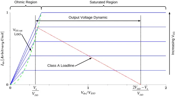
II-2 Power stage design ... 42
II-2.1. LDMOS transistor model ... 43
II-2.2. Design parameters ... 43
II-2.3. Classes of operation ... 45
II-2.4. Saturated PA ... 52
II-2.5. Linear PA ... 56
II-3 Output matching network design ... 59
6
II-4.1. Switched capacitor bank ... 62
II-5 RF switch design ... 64
II-5.1. SP1T ... 65
II-5.2. SPnT ... 66
II-6 Conclusion ... 67
II-7 References ... 68
Chapter III: Reconfigurable Multi-Mode Multi-Band Power Amplifier Design ... 69
III-1 Introduction ... 69
III-2 Reconfigurable MMPA architecture ... 70
III-3 Reconfigurable MMPA design ... 71
III-3.1. Reconfigurable power stage design ... 71
III-3.2. Reconfigurable output matching network design ... 76
III-3.3. Driver stage design ... 87
III-3.4. Input matching network design ... 89
III-3.5. Inter-stage matching network design ... 90
III-3.6. Reconfigurable MMPA line-up implementation ... 93
III-4 Measured performances ... 94
III-4.1. Power amplifier characterization ... 95
III-4.2. Output matching network characterization ... 97
III-4.3. MMPA line-up characterization ... 99
III-5 Conclusion ... 100
III-6 References ... 101
Chapter IV: Study of High Efficiency PA architectures ... 103
IV-1 Introduction ... 103
IV-2 PA efficiency enhancement ... 103
IV-2.1. Efficiency enhancement limitations ... 104
IV-3 Supply and load modulation PA design ... 105
IV-3.1. Envelope Tracking ... 105
IV-3.2. Load Modulation ... 108
IV-4 Design and implementation of a load modulated PA architecture ... 110
IV-5 Conclusion ... 119
IV-6 References ... 120
Conclusion and perspective ... 121
7
International conferences ... 123
National conferences ... 123
Appendices ... 125
Appendix A: Fourier Coefficient Calculations ... 125
Appendix B: Current and voltage coefficients calculation in non-sinusoidal classes ... 136
Appendix C: Determination of the input impedance of a transistor according to the degeneration inductance ... 138
Appendix D: Calculation of the required transistor width in a switched capacitor branch ... 141
Appendix E: Determination of the capacitance of a second harmonic trap not interfering with the fundamental impedance ... 142
Appendix F: Calculation of the trap capacitor according to the trap inductance and parallel impedance ... 143
Appendix G: Calculation of the minimum Q-factor of a binary weighted switched capacitor bank... 144
Figure index... 147
Table index ... 153
List of acronyms and abbreviations ... 155
Abstract ... 157
9
Introduction
During the last two decades, the cellular telecommunications have been expanding exponentially. This expansion has mainly been driven by the consumer needs for more diverse services. Each service addition was carried by a new standard generation. Furthermore, the obsolescence of old radio services, such as Terrestrial Analog Television, has released frequency bands that have been recently reallocated to cellular applications.
Following these trends, cellular devices are becoming more and more complex. The Front-End Module (FEM), which is the interface between the RF transceiver and the antenna, has to cope with the new standards (4G) while maintaining the compatibility with the former ones (2G, 3G). Inside the Front-End Module, the Power Amplifier (PA) is a major contributor to the performance of the FEM, but also to its complexity and energy consumption. Nowadays, a FEM can be required to address more than 10 frequency bands among all the current standards, often meaning numerous PA. Furthermore, the PA is required to be highly energy efficient.
Reducing the complexity and consumption of FEM can be done by using new PA architectures. Those architectures should handle several standards and bands using a limited number of PA with maximal efficiency in every operating mode. Reconfigurable PA seems to be promising for coping with these constraints and they are currently a major research subject.
While the traditional GaAs based technologies offer high PA performances, SOI CMOS technology offers a promising path for further integration of reconfigurable PA at reduced cost.
This thesis focuses on study and integration of a reconfigurable multi-mode multi-band power amplifier (MMPA) in SOI CMOS 130nm technology. The original solution proposed in this work represents a significant step toward the integration of high efficiency MMPA for cellular handset applications. This manuscript is divided in four chapters.
The First Chapter begins with a presentation of the context of this work. Issues associated with MMPA and performances of traditional MMPA architectures are introduced. The SOI CMOS technology used in this work for MMPA integration is also presented with a focus on the available power devices and passive elements.
In the Second Chapter, PA performances are first defined. A design methodology for saturated and linear PA integration is then proposed. Matching networks are critical for optimal PA operation. In order to realize tunable matching networks, tunable capacitors and mode switches are required. The design methodology of such devices is presented while ensuring the performance of the full architecture.
The Third Chapter focuses on the design of a new reconfigurable MMPA architecture and its integration in SOI CMOS.A focus is made on a reconfigurable power device and its implementation. Reconfigurability presents serious challenges for the design of PA the line-up and to ensure correct performance of the proposed architecture the required tradeoffs are presented. Then, implementation and measurement results of the developed SOI CMOS MMPA are presented and compared to state of the art.
The last Chapter presents a comparative study of two different high efficiency PA architectures based on supply and load modulation. The goal of this study is to determine the applications for which each technique is advantageous, both in terms of efficiency and linearity. Lastly, the design and SOI CMOS implementation of passive load modulation PA architecture is proposed. This demonstrator targets watt-level output power with high back-off efficiency improvement for cellular femto cell applications.
11
Chapter I: Context
I-1
Introduction
The first part of this chapter will present a brief history of cellular telecommunications from the second generation (2G) up to the current fourth generation (4G). The front-end module constraints associated with each standard will be given.
The second part will present the Front-End module with a focus on the power amplifier. Three power amplifier architectures, from the simplest Mode Specific architecture to the more advanced Converged architecture, will be presented. Afterwards, reconfigurable power amplifiers will be introduced.
The last part gives an overview of the SOI-CMOS 130 nm technology (STMicroelectronics) which has been chosen for the implementation of the designed circuits.
I-2
Cellular telecommunications evolution
Since the first deployment of cellular networks in the 80s, a lot of changes have been introduced in the cellular world. This first part will give information on the gradual transformation of mobile telecommunication standards with a focus on European Standards.
I-2.1. 2Gstandards
During the ‘90s, the cellular telecommunication market exploded. The users from the first generation (1G) analog standard rapidly saturated the cellular networks and the analog encoding was showing its limits in terms of data rate and security. At that time, two standards were studied: The Interim Standard 95 (IS-95, also called CDMA-One) developed by Qualcomm in the USA in the 900MHz and 1950MHz AMPS bands, and the Global System for Mobile Communications (GSM) introduced by the European Telecommunication Standardization Institute (ETSI) for the 835 MHZ and 1800MHz TACS bands.
The first breakthrough compared to the first generation was the use of more robust digital encoding compared to 1G. In the GSM standard, frequency duplex is used to differentiate between uplink and downlink transmission and Time Division Multiple Access (TDMA) is used to share each channel between 8 users. IS-95 takes advantage of Code Division Multiple Access (CDMA) to differentiate uplink and downlink communication and to share each channel between users. GSM is the most widespread 2G standard while IS-95 and its evolutions are only located in Northern America.
In the late 90’s GSM was improved to General Packet Radio Service (GPRS), which allowed taking advantage of unused slots in order to improve the data rates. Later, in 2003, the Enhanced Data-rate for GSM Evolution (EDGE) was deployed. Using a new modulation scheme, its data rate is further improved.
Table 1: Characteristics of TX signals for GSM handsets.
Standard Output Power @ antenna Modulation
GSM (Low Band) 33dBm
GMSK (Constant Envelope)
GSM (High Band) 30dBm
2G standards are still used nowadays for their robustness and capability to maintain communication on long ranges. However the evolution towards higher data rates has been allowed thanks to the introduction of 3G standard.
12
I-2.2. 3G standards
With the users starting to use their equipment in everyday life, more and more services were developed, especially media streaming and faster internet connections. In the beginning of the 21st century, Japan launched the first 3G standard: Wideband Code Division Multiple Access
(W-CDMA). In the US, the evolution favored the CDMA 2000 standard, as an evolution of IS-95. The first major change with 3G was the allocation of new bands (around 2GHz). In the case of WCDMA, those bands were split in 5MHz channels and more complex Quadrature Amplitude Modulations (QAM) were introduced. By further improving controls, High Speed Packet Access (HSPA) was developed to improve data rates. Evolved HSPA (HSPA+) unlocked even higher data rates with QAM 64 and the introduction of Multiple Input Multiple Output (MIMO) systems.
Table 2: Characteristics of TX signal for 3G handsets.
Standard Output Power @ antenna Modulation PAPR
W-CDMA Release’99
24dBm HPSK (Amplitude & phase) 3.5dB
HSUPA QAM (Amplitude & phase) 6.6dB
Today 3G is widely deployed around the world in urban areas where most of the population is concentrated. Following on its momentum, the search of even higher data-rates continued with the introduction of 4G standard.
I-2.3. 4G standards
4G marks the beginning of the Voice over IP (VoIP) in cellular communications. It should also be capable of supporting High Definition (HD) video streaming. For all these reasons, 4G must have access to very high mobile data rates. Two standards were created. First, World interoperability for Microwave Access (WiMAX) is the solution of the Institute of Electrical and Electronics Engineering (IEEE) and is a group of standards around mobile telecommunications. In Europe, the 3rd Generation
Partnership Project (3GPP) developed a second solution: Long Term Evolution (LTE) standard which uses an Orthogonal Frequency Division Multiple Access (OFDMA). However, having difficulties to reach the required data rates, only LTE-Advanced (LTE-A) is considered as a 4G standard. 4G standards are characterized by a very high PAPR. The high PAPR is due to the efficient use of the spectrum to increase the data rates. Another specificity of LTE is the ability to adjust the bandwidth available per user between 1.4MHz and 20MHz according to the load on the network to further optimize the data-rate per user. Table 3 gives the equivalence between bandwidth and the number of Resource Blocks (RB) for LTE signals. Carrier aggregation technique, which has been introduced with LTE-A, is outside the scope of this work and is therefore not mentioned here.
Table 3: Bandwidth and Resource Blocks for LTE signals.
Bandwidth 1.4MHz 3MHz 5MHz 10MHz 15MHz 20MHz
Maximum Resource Blocks 6 15 25 50 75 100
Table 4: Characteristics of TX signal for 4G handsets.
Standard Output Power @antenna Modulation PAPR
LTE 24dBm QAM/QPSK >6dB
Another major change with 4G is the increased number of frequency bands. As some obsolete wireless applications are no longer used, spectrum resource is freed. The new available bands are then redistributed among new applications such as 4Gcommunications. Figure 1shows all the Evolved Universal Terrestrial Radio Access (E-UTRA) Bands defined nowadays.
13
Figure 1: E-UTRA frequency bands (Uplink).
The graph shows 5 major frequency domains: Very Low Band (VLB), Low Band (LB), Mid-Band (MB), High Mid-Band (HB) and Very High Mid-Band (VHB). In total, there are 39 bands when grouping Frequency Division Duplex (FDD) bands– B1 to B31– and Time Division Duplex (TDD) – B33 to B44. In this thesis, the focus is made on the LB FDD bands (700-920MHz). Note that the methodologies presented further in this thesis can be transposed to higher frequency bands. Therefore, studying other bands does not add further research interest.
The user equipment has to follow the trend and the next part emphasizes on the consequences of this evolution on Front-End Module (FEM) and Power Amplifier Module (PAM) architectures.
I-3
Cellular RF Front End
I-3.1. RF Front End Module (FEM)
Nowadays, several RF blocks are required in a wireless cellular terminal. The RF transceiver is composed of all the elements required to either generate the RF signals containing the information to be transmitted, or decode the information by processing a received signal. The antenna is the frontier between the electric world and the radio waves.
B1 B2 B3 B4 B5 B7 B8 B9 B10 B11 B12 B13 B17 B18 B19 B20 B21 B22 B23 B24 B25 B26 B27 B28 B30 B31 B33 B34 B35 B36 B37 B38 B39 B40 B41 B42 B43 B44 B14 Low Band (LB) Mid-Band (MB) High Band (HB)
Very High Band (VHB)
Very Low Band (VLB)
14
Figure 2: Multiband 2G/3G/4G FEM for FDD applications.
The RF Front-End Module (FEM), as shown in Figure 2, is the module that realizes all the operations between the transceiver and the antenna. It includes filters to select the frequencies that will be transmitted or received by the antenna, power amplifiers (PA) and RF switches. The Low Noise Amplifiers (LNAs), which are generally included in the transceiver, are used to obtain the desired sensitivity.
The RF FEM includes all the necessary circuitry to support different standard and bands. In this example, the transmit path (TX) for 2G is handled using a quad-band GSM PA associated with a High Band (HB) and Low Band (LB) low pass filters to limit the harmonics level. The receive path (RX) for 2G includes two Low Noise Amplifiers (LNA), one for the HB path and another one for the LB path. For 3G and 4G, the uplink and downlink communications are done simultaneously using Frequency Domain Duplex (FDD). Duplexer filters are used to separate TX and RX signals. Having more standards and bands to support means more RF circuits and brings new design challenges for the RF FEM. In this thesis, we will focus on the power amplifiers.
B a s e b a n d & R F T ra n s c e iv e r 4 Band GSM PA GSM HB TX GSM LB TX 3G B1 TRX 3G B8 TRX 3G B2 TRX 4G B12 TRX 4G B7 TRX GSM HB RX GSM LB RX SP9T LNAs included in the transceiver
15
I-3.2. RF Power Amplifier Module (PAM)
PA modules are essential in radio links since the transmit RF signal needs to be amplified at a high enough level to ensure quality of the transmission. Traditionally, PA modules (PAM) were optimized for a dedicated operation. However, with the growing number of standards, this strategy is reaching its limits in terms of cost and complexity [Walsh09]. In the following paragraphs, the evolution of multimode multiband PAM architectures will be discussed.
A. PAM architectures
a. Mode Specific PA architecture
Historically, when a new band or standard was required, the manufacturers simply added a discrete “mode specific” PA line-up in the RF FEM, as shown in Figure 2. The advantage of such approach is to have the best performance for each mode/standard while paying for exactly what is required.
Table 5: Performance of commercial “Mode Specific” Power Amplifiers.
Reference Standard Output Power Power Added Efficiency
[SKY77351-13] 2G (GSM) 35.5dBm 55%
[SKY77187] 3G (HSPA) 29dBm 40%
[SKY77709] 4G (LTE) 28dBm 36%
With the current evolution trend, this solution tends to be abandoned in favor of converged architectures which are more cost effective.
b. Converged PA architecture
In a converged PA architecture, the goal is to minimize the number of PA line-up while addressing multiple standard and frequency bands [Cheng11]. The block diagram of a converged PA architecture is shown in Figure 3.
Both PA line-ups must be able to reconfigure their operating mode according to the considered standard and frequency band. Tuning degrades to the performance of line-ups. Examples of performance for this type of PA are given in Table 6.
Table 6: Performances of converged 2G/3G PA with support of bands 5 and 8 [Kang13].
Mode Pout PAE ACPR
2G (GSM) 34.5dBm > 53% -
2.5G (EDGE) 29.0dBm > 27% -58dBc
3G (WCDMA) 28.2dBm > 41% -39dBc
Figure 3: Converged PA Architecture.
3G/4G-B1 3G/4G-B2 4G-B7 3G/4G-B8 4G-B12 2G-HB 2G-LB
16
To implement such architecture, either wideband or reconfigurable PA is required. Wideband power amplifiers have the advantage to minimize the complexity but have degraded performance due to the required broadband matching networks. On the other hand, reconfigurable PA (RPA) offer better performance in every band at the cost of a higher complexity since tunable components are needed.
B. Reconfigurable PA
a. Reconfigurable multi-mode PA
As discussed in previously, the different cellular standards have different types of requirements. GSM standard requires high output power with low linearity constraints. Therefore, highly efficient saturated PAs operating near saturation can be used. Others standards, such as LTE, require lower power with high PAPR and linearity constraints. For this last application, linear PAs operating in linear mode are required.
PA with different operating modes (saturated or linear) is called multimode PA. Such PA can be realized by adjusting the bias, as shown in Figure 4[Kang08].
Figure 4: Multimode PA with saturated and linear operating modes [Kang08].
In this architecture, the bias current of the driver and output stages are adjusted according to VMODE to operate in either linear or saturated mode. When operating for 2G signals (GSM), the
bias is adjusted in both stages to maximize their efficiency and output powers. If the PA is required to operate linearly, for 2.5G (IS-95 CDMA) for instance, the two stages are biased for higher linearity at the expense of efficiency.
Improved multimode architectures make use of reconfigurable matching to adjust the load of the power stage and transistor sizing to achieve optimized performance for both operations [Kang13]. The schematic of such reconfigurable multimode PA architecture is depicted in Figure 5.In GSM mode, for which high power and efficiency are required, both Q3 and Q4 transistors participate to signal amplification and the Output Matching Network (OMN) is configured for 2 while Path-1 is in a high impedance mode. For 3G operation (UMTS), Q4 is switched-off and Q3 is the only active transistor of the output stage. The OMN is switched to Path-1 with Path-2 set to high impedance mode. In this configuration, the output stage is loaded by the optimal impedance for linear operation.
17
Figure 5: Reconfigurable multimode PA with transistor sizing and reconfigurable matching network [Kang13].
A summary of the performance of the two architectures is given in Table 7.
Table 7: State-of-the-art of reconfigurable multimode PA [Kang08] [Kang13].
Work Operating Frequency GSM Output Power GSM Efficiency Linear Standard Linear Output Power Linear Efficiency Technology [Kang08] 1880MHz 32.5dBm 64.7% IS-95A CDMA 28dBm 39% InGaP/GaAs 2 µm HBT [Kang13] 900MHz 850MHz 34.5dBm 53.55% Release’99 W-CDMA 28.2dBm 41% InGaP/GaAs 2 µm HBT / PIN diode
Both PAs are adjusted for operating mode and power level in accordance with the targeted standard. In linear mode, both PA architectures meet a good tradeoff between linearity and efficiency.
b. Reconfigurable multi-band PA
As mentioned in section I-3.2.A.b, the trend for PA is to support several frequency bands with the same circuitry. The use of tunable matching networks allows such multiband PA solutions [Aref12] [Kang13].
In Figure 5, Path-1 for UMTS (3G) includes a frequency reconfigurable network (FRN) which allow PA performances optimization for 900MHz (SW #3 open) or 850MHz (SW #3 closed)..
In Figure 6 [Aref12] another multiband PA architecture using several reconfigurable matching elements is proposed. According to the number of shunt capacitors activated in the Tunable load Transformation network, this multiband PA architecture can be tuned from 1.6 GHz to 2.6 GHz, with optimal operation from 1.7 GHz to 2.1 GHz.
18
Figure 6: Simplified schematic of a multiband saturated PA [Aref12].
c. Reconfigurable PA with multiple power levels
1. Back-off efficiency
One of the major challenges of the 21st century for cellular application is the enhancement
of PA efficiency. For cellular networks it is required to produce components compliant with environmental norms and consuming power only when required. In handset application, talk-time and battery life time are directly affected by PA power consumption, PA being one of the most power consuming block of the FEM. Therefore the PA must operate with the highest possible efficiency. Traditional PA architectures are optimized to be the most efficient at maximum power (Pmax). Figure 7 shows the Power Added Efficiency (PAE) of a traditional PA as a function of output power (Pout).
Figure 7: PAE vs. Output Power (Pout) for a traditional PA architecture.
Pmax
6 dB Back-off
19
In this graph we can notice that efficiency drops for low output power levels. In this example, if the required power is four times lower (6dB power back-off) than Pmax, PAE is reduced by a factor of two.
For constant envelope signals, PA linearity is not a concern and the PA line-up can be reconfigured in static manner to optimize its efficiency at each back-off power. PA efficiency can be optimized for different power levels while using multi-state architecture as shown in Figure 8.
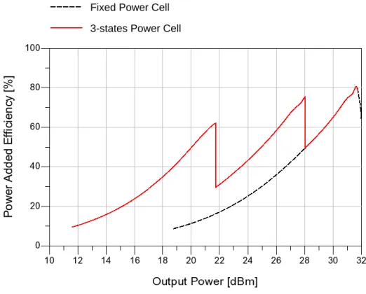
Figure 8:PAE evolution vs. Output Power in a multi-power mode PA
Generally, the use of 3 states is sufficient for a correct improvement of efficiency. The added circuitry is simple and easy to drive. The static reconfiguration of PA efficiency is commonly done with transistor re-sizing and stage bypass architectures.
2. Power transistor re-sizing
One type of PA architecture takes advantage from the bias strategy of segmented power devices. For a given power level, only the minimum number of power cell is biased [Kim04] [Kim11a]. The unused power cells are switched off to improve the overall efficiency of the PA. The block schematic of a PA architecture with power transistor re-sizing using 2 output cells is presented in Figure 9.
Fixed Power Cell 3-states Power Cell
20
Figure 9: PA architecture with power transistor re-sizing.
In this example, when the PA is required to deliver the maximum output power, both cells are used. If half of the power is required, one cell is switched off by switching its input to ground. A drawback of this architecture is that the output impedance of the switched cell can disturb the active cell. Therefore, the combining node must be carefully designed. Table 8 gives some state-of-the-art performances for such architecture.
Table 8: State-of-the-art PA architecture with power transistor re-sizing.
Work Maximum Output Power (Pmax) Efficiency at Pmax Back-off power (PBO) Efficiency at PBO Efficiency Improvement * Technology [Kim04] 27dBm 36% 16dBm 15% +83% InGaP/GaAs HBT [Kim11a] 31dBm 34.8% 20dBm 14% +43% 0.18 µm CMOS * Comparing the back-off efficiency of architecture with and without transistor re-sizing
3. Stage bypass
Instead of segmenting the active device and switching off unused power cells, it is possible to implement several line-ups in the same PA architecture. Each line-up is optimized for a given power range. By switching between these line-ups, or bypassing them, the PA can have optimal efficiency at different power levels. Examples of PA architectures using stage-bypass are shown in figure 10.
Figure 10: PA stage bypass using line (left) or switch (right).
C o m b in in g N o d e Output Stage RFin RFout Driver Stage RFin RFout
High Power Path
Low Power Path
Switched Paths Architecture
Output Stage RFin
Driver Stage
RFout
Bypass Line
21
In the first example (left), the output stage is switched off for low power operation and the bypass line transfers the signal directly from the driver stage to the PA output [Kang13]. In this type of architecture, special care must be taken when designing the bypass line to minimize its influence in high power mode. In high power mode, the impedance of the bypass line is several times higher than the load impedance of the output stage and the input impedance of the output stage is lower than the input impedance of the bypass line. In low power mode, when the output stage is deactivated, the input and output impedance of this stage become higher than that of the bypass line.
In the second example (right), two PA line-ups are present and have been optimized independently for either high power of low power operation [Jun13]. The switches are used to select one path or the other according to the required power, the unused path being biased off. In this case, the switches are sized to have minimal loss in both modes. Switches can be used to bypass stages, line-ups or even both [Hau10]. Table 9 gives a state-of-the-art of different stage-bypass PA architectures.
Table 9: State-of-the-art of Stage-bypass PA architectures.
Work High output power (Phigh) Efficiency at Phigh Low output power (Plow) Efficiency at Plow Total Efficiency Improvement * Technology [Hau10] 28.5bdBm 42% 17dBm 22% +175% InGaP/GaAs HBT + pHEMT switches [Jun13] 26dBm 28% 16dBm 16% +86% 0.35 µm SiGe BiCMOS [Kang13] 28.2dBm 41% 16dBm 17.4% +117% InGaP/GaAs 2 µm HBT + PIN diode * Comparing the back-off efficiency of architecture with and without stage bypassing
Transistor re-sizing and stage bypass architectures offer good improvement but are limited when used to amplify varying envelope signals. With such signals, the PA suffers from efficiency degradations as shown in Figure 11 since the average power (Pavg) of the modulated signal is lower than the peak power (Ppeak) where efficiency is maximized.
Figure 11:PAE evolution vs. Output Power in a traditional Power Amplifier
Ppeak
Pavg
22
As can be seen, the PA operates most of the time at back-off power. In this graph, the efficiency at Pavg is decreased by 50% compared to the maximal efficiency. The following equation gives the expression to calculate the average efficiency when amplifying a modulated signal [Popovic14].
〈𝑃𝐴𝐸〉=∫𝑃𝐷𝐹(𝑃𝑜𝑢𝑡)∙ 𝑃𝐴𝐸(𝑃𝑜𝑢𝑡)𝑑𝑃𝑜𝑢𝑡
∫𝑃𝐷𝐹(𝑃𝑜𝑢𝑡)𝑑𝑃𝑜𝑢𝑡 Equation 1
Using this equation, it is possible to see that average efficiency of the PA optimized at the maximum output power will be degraded when amplifying a signal using a complex modulation. To improve the efficiency of the PA, it becomes necessary to improve the instantaneous efficiency by providing dynamic reconfiguration of PA characteristics.
d. High efficiency PA architectures
PA architectures based on supply or load impedance modulation allow dynamic efficiency enhancement.
Figure 12: Block schematic of high efficiency PA architecture [ref]
Such PA architecture can be represented by the block diagram shown in Figure 12 and inspired by [Popovic14]. The power amplifier is the main cell of the architecture. The auxiliary block allows control of PA supply or load impedance. The separation block divides the input signal in two parts. The first one is the signal to be amplified by the power amplifier. The second part is the information used by the auxiliary block to realize control. The actuation takes place in the combination block. The actuation signal optimizes the operation of the power amplifier to achieve high efficiency.
1. Supply modulation
i. Envelope Tracking
The envelope tracking power amplifier (ETPA) takes advantage of an Envelope Amplifier to modify the supply voltage of a linear PA according to the envelope level[Yan11][Kim11b]. The simplified schematic of an ETPA is shown in Figure 13.
S e p a ra to r C o m b in e r Auxiliary Block Power Amplifier
23
Figure 13: Block schematic of Envelope Tracking Power Amplifiers
The Envelope Detector is used to extract the envelope of the input RF signal. While the power amplifier amplifies the RF signal, the envelope amplifier shapes the supply signal VDD to
optimize PA efficiency as a function of envelope level. The relation between the varying envelope RF signal and varying supply signal is called envelope shaping. Different shaping strategies can be adopted to optimize PA performances. The recombination consists in applying the shaped supply voltage to the power amplifier supply input. The output signal of the ETPA is therefore an amplified version of the input signal with an optimized DC consumption.
The synchronization of the variable supply voltage and RF signal should be ensured to limit non-linearity. Efficiency of the envelope amplifier is critical since efficiency of the ETPA is given by Equation 2.
𝜂𝐸𝑇𝑃𝐴= 𝜂𝑃𝐴∗ 𝜂𝐷𝐶/𝐷𝐶 Equation 2
From this equation, it can be seen that low efficiency of the envelope amplifier can lead to lower overall efficiency than the PA in a stand-alone configuration.
ii. Envelope Elimination and Restoration
Figure 14: General schematic of the Envelope Elimination and Restoration Power Amplifier
Envelope Detector Output Matching Envelope Amplifier Linear Power Amplifier Output Matching Envelope Amplifier Saturated Power Amplifier AM PM
24
The block schematic of an Envelope Elimination and Restoration (EER) PA is shown in Figure 14. This architecture is very similar to the envelope tracking. There is however significant differences in its operation. The EER PA uses a total separation of the Amplitude Modulation (AM) and Phase Modulation (PM) of the complex signal [Pinon08] [Kim10]. The AM signal is sent to the envelope amplifier to generate the supply signal of a saturated PA. The DC/DC converter in the case of EER has more precision constraint than ETPA as the shaped supply is used to restore the AM component of the modulation to the output signal.
The PM signal is amplified by the PA. As this signal has a constant envelope, the PA can be designed for a highly efficient switching class. The full modulation is restored thanks to the supply voltage of the PA which will be the image of the signal Envelope. Synchronization between the shaped supply and the amplified PM signals is crucial. The least synchronization issue can lead to high distortion of the output signal. Also, the efficiency of the envelope amplifier cannot be neglected in the overall efficiency of an EER PA, as it was the case for the ETPA.
2. Load Modulation
i. Doherty Power Amplifiers
The Doherty Amplifier uses an “active load-pulling” mechanism. The block schematic of the architecture is shown in Figure 15. Two power cells are required in Doherty Amplifiers [Kitahara11] [YuTing14]. The main amplifier is designed for Class-AB operation. The peaking amplifier is biased for a more efficient Class-C operation.
Figure 15: Block schematic of Doherty Amplifiers
Between low to medium power levels, the peaking amplifier is off while the Class-AB main amplifier is operating alone. Once the main amplifier reaches it saturation output level, the peaking Class-C amplifier turns on. As it occurs, more current is flowed into the load and, and then the load viewed by the main amplifier through the quarter-wave transformer decreases. As the load viewed by the main amplifier is decreased, the current delivered by this amplifier increases while the voltage is maintained to its maximum value. Doing so increases the dynamic of the main amplifier towards high power.
Doherty Amplifiers requiring two amplifier stages, the surface area can be significant. Moreover, the need for quarter-wave transformers does not facilitate the integration of such architecture.
Main Amplifier
(Class AB)
Peaking Amplifier
(Class C)
λ/4
λ/4
25
ii. Passive Load Modulation
The passive load modulation is the passive equivalent of the Doherty Amplifier. The general schematic of such architecture is given in Figure 16.
Figure 16: Passive Load Modulation Power Amplifier block schematic
This architecture relies on a Tunable Matching Network (TMN) to modify the load impedance viewed by the PA [Yue12] [Andersson12]. The TMN is actuated by a control signal generated from the envelope information. This can either be done by detecting the envelope of the RF signal or by directly using the baseband information.
𝜂𝑡𝑜𝑡= 𝜂𝑃𝐴+𝐶𝑇𝑅𝐿∙ 𝐼𝐿𝑇𝑀𝑁=𝑃 𝑃𝑜𝑢𝑡
𝐷𝐶𝑃𝐴+ 𝑃𝐷𝐶𝐶𝑇𝑅𝐿∙ 𝐼𝐿𝑇𝑀𝑁 Equation 3
The drawback of this technique is the increased loss in the TMN compared to a fixed network. A rough estimation of the loss impact is given in Equation 3. In this formula, the efficiency of the power amplifier should include the consumption of the control processing block PDC CTRL. Moreover, the loss of the TMN (ILTMN) should not be too high in order to not decrease the overall efficiency. Furthermore, bad synchronization between the TMN actuation and RF signal can lead to distortion in the RF signal.
3. Impact on linearity
All the architecture presented above can distort the signal. In that case, a linearization technique can be added in order to meet the linearity requirement of the considered standard. The consumption of the linearization circuit impacts the efficiency of the full architecture. In the case of handset PA, the consumption of the linearization circuit mitigates the efficiency enhancement [Cripps06].
Table 10presents a state-of-the-art of high efficiency PA architectures using supply and load modulation, for both handset and base station applications.
Envelope Detector TMN Power Amplifier Control Processing
26
Table 10: High efficiency PA architecture with supply/load modulation.
Work Architecture Application
Max. Output Power (Pmax) Efficiency at Pmax Back-off Efficiency at Back-off [Kitahara11]
Doherty Base Stations 55dBm 50% 8dB 48%
[YuTing14] 54.7dBm 56% 6dB 48% [Yue12] Load Modulation 40.4dBm 60% 7.5dB 60% [Andersson12] 38dBm 60% 8dB 45% [Yan11] Envelope Tracking 41dBm 63% 11dB 57% [Kim11b] Handset 33dBm 66% 10dB 62%
[Pinon08] Envelope Elimination & Restoration
28dBm 61% 8dB 48%
[Kim10] 27dBm 59% 7dB 54%
As can be seen in the table, PA efficiency can be highly improved using those architectures. Reconfigurable power architectures improve power amplifier and either the supported modes, bands or power level. By using new technologies for implementing reconfigurable power amplifiers, better integration and cost reduction can be achieved, as shown in the next section.
I-4
SOI CMOS technology overview
Today, the main technology used in PA design for handset applications is GaAs HBT since it offers the best PA performance in terms of output power, gain, efficiency and linearity. However its main drawback is a lower yield and a higher cost compared to Very Large Scale Integration (VLSI) Silicon technologies. Furthermore, the co-integration of digital control circuitry is not realistic in GaAs. Table 11 summarizes the advantages and drawbacks of different PA integration technologies.
Table 11: Technology Comparison.
Technology Cost Passive Quality Factor RF Power Device Performance Digital Performance
CMOS ++ - - - +
BiCMOS + - - + +
SOI CMOS + - + ++
GaAs HBT - - - ++ -
Module ++ ++ N/A N/A
27
Figure 17: Used technologies in high performance FEM [ASN13].
In this module, there are 2 GaAs PAs for linear operation and a quad-band CMOS PA for GSM. The control part is implemented either in a Silicon on Insulator (SOI) or Bulk CMOS technology, as cost effective technologies for digital integration. Matching networks use Surface Mounted Device (SMD) capacitors and distributed lines on the laminate substrate of the module. Duplex filters (DPX) are implemented using Surface Acoustic Wave (SAW) or Bulk Acoustic Wave (BAW) technologies. Acoustic Wave technologies are currently the most effective solutions to realize low insertion loss and high TX/RX isolation with sharp band edges.
The combination of all these different technologies implies added assembly costs for the manufacturers. In order to reduce this assembly costs, the use of a single technology with competitive performances and lower cost compared to GaAs and high integration capabilities appears necessary. Recent progresses in SOI CMOS technologies make this technology a good candidate for PA/FEM integration [Andia10].
I-4.1. RF devices
A. RF switch
SOI NMOS devices allow implementation of low loss and high isolation RF power switches [Carrara09]. Switch performances are related to the on-state resistance (Ron) and off-state
capacitance (Coff) of NMOS devices. In this work, a SOI CMOS 130nm process with six metal layers
has been used. This industrial SOI CMOS process from STMicroelectronics presents a Ron.Coff product of 310fs with on-state resistance of 1Ω.mm.
B. LDMOS transistor
The Laterally Diffused MOS (LDMOS) transistor allows high voltage operation with high robustness thanks to the drain extension [Reynier09] and is becoming more and more prominent in the field of RF power applications. In the selected SOI CMOS technology, the LDMOS transistor is characterized by a transition frequency (Ft) of 36GHz and a breakdown voltage (BVds) of
CMOS PA GaAs PA GaAs PA SOI-CMOS Switch SOI-CMOS Switch SOI-CMOS Switch CMOS/SOI-CMOS Control PCB & SMD Matching Components
28
13V[ST15].A cross-section view of this device is shown in Figure 18.With this power device, high efficiency PA has been demonstrated [Giry13].
Figure 18: Cross-section of a LDMOS transistor.
C. Inductors
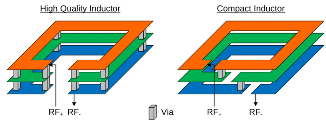
In cellular PA applications, wavelength is too high (few centimeters) to obtain high inductance values using transmission lines. Planar inductors with high quality factor (Q) can be obtained in SOI CMOS technology thanks to the high resistivity substrate [Andia10]. Planar inductors can be realized with two distinct approaches, as shown in Figure 19.
Figure 19: Simplified structure of a high Q inductor (left) and compact inductor (right) implemented with 3 metal layers and 1 turn per metal level.
The high Q implementation (left in Figure 19) uses metal stack to achieve low ohmic loss. Combined with wide lines, such inductors can achieve high quality factors (>10). However, they tend to be area consuming and are generally limited to low inductance values (<2nH).
The compact implementation (right in Figure 19) takes advantage of the multiple metal layers available in the technology. By realizing one elementary coil per layer and then connecting the layers in series, it is possible to implement high inductance values (>5nH). The drawback of this implementation is the high series resistance, leading to limited quality factors (<5). These inductors are generally used for RF/analog blocks where insertion loss is not critical.
High resistivity P Substrate
Buried Oxide P b o d y P+ N+ N+ N epitaxy N epitaxy N+ N+ Oxide Oxide D S D G G Drain extension Access Zone P b o d y Channel Compact Inductor RF -RF+
High Quality Inductor
RF
29
D. Capacitors
In this work, Metal-Insulator-Metal (MIM) and Metal-Oxide-Metal (MOM) capacitors have been used.
Figure 20: MIM capacitor (left) and interdigitated MOM capacitor (right).
MIM capacitor (left in Figure 20), is a vertical structure. It uses a high dielectric constant insulator material between a metal top plane and a metal bottom plane to realize compact high capacitance values. The drawback of this structure is the low break-down voltage (<10V). These capacitors can be used for analog blocks or low voltage RF path.
Interdigitated MOM capacitor (right in Figure 20) is a horizontal structure composed of interdigitated metal fingers. This structure is less compact than MIM capacitor, due to the lower dielectric constant of the oxide, but offers very high breakdown voltages (>50V). For high power RF paths, the MOM capacitor is preferable to MIM capacitor thanks to its inherent higher breakdown voltage.
I-4.2. Through Silicon Via
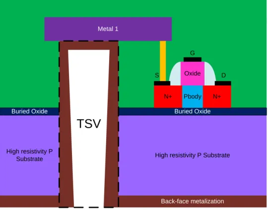
Through Silicon Via (TSV) can be realized after post-processing of SOI CMOS wafers as shown in Figure 21. MIM Capacitor Insulator TOP plate BOTTOM plate RF+ RF -Via RF -RF+ MOM Capacitor
30
Figure 21: Simplified Cross-section view of a TSV connected to the source of a MOS transistor.
Power amplifiers suffer from parasitic inductor to ground which lead to performance degradation. Thanks to TSV inductance to ground can be drastically reduced. Another beneficial effect of TSV is the mitigation of thermal issues. The high performance of SOI is obtained thanks to the buried oxide which isolates active devices from the silicon substrate. This is however done at the cost of thermal dissipation, which leads to increased temperature and can degrade the time to failure of active devices. TSV copper metallization offer a low thermal path to the backside of the chip.
I-5
Conclusion
Multiple cellular standards and frequency bands have emerged over the past 3 decades and today Front End Modules and Power Amplifier Modules face increasing challenging requirements. Current PA architectures are limited and reconfigurable PA appears as a good candidate to address multimode multiband requirements with reduced size and cost. Therefore, design and implementation of a reconfigurable MMPA in SOI CMOS technology is proposed in the following part.
High resistivity P Substrate Buried Oxide Pbody N+ Oxide D S G High resistivity P Substrate Buried Oxide N+ Metal 1
TSV
Back-face metalization31
I-6
References
[Andia10] L. Andia Montes, “Amplificateur de puissance en classe commuté pour application dans un émetteur multiradio à haut rendement”, Ph. D. Thesis, Université Paris-Est, 2210.
[Andersson12] C. M. Andersson, D. Gustafsson, K. Yamanake, E. Kuwata, H. Otsuka, M. Nakayama, Y. Hirano, I. Angelov, C. Fager, & N. Rorsman, “Theory and Design of Class-J Power Amplifiers With Dynamic Load Modulation”, IEEE Transactions on Microwave Theory
and Techniques, vol. 60, pp. 3778-3786, December 2012.
[Aref12] A. F. Aref & R. Negra, “A Fully Integrated Adaptive Multiband Multimode Switching-Mode CMOS Power Amplifier”, IEEE Transactions on Microwave Theory and
Techniques, vol. 60, pp. 2549-2561, August 2012.
[ASN13] Advanced Substrate News, “ASN Exclusive Interview: Skyworks on SOI for RF”, Semiconductor Manufacturing and Design community website, 2013, retrieved from http://semimd.com/hars/2013/12/04/asn-exclusive-interview-skyworks-on-soi-for-rf
[Carrara09] F. Carrara, C. D. Presti, F. Pappalardo & G. Palmisano, “A 2.4-GHz 24-dBm SOI CMOS Power Amplifier With Fully Integrated Reconfigurable Output Matching Network”,
IEEE Transactions on Microwave Theory and Techniques, Vol. 57, No. 9, pp.
2122-2130, September 2009.
[Cheng11] N. Cheng & J. P. Young, “Challenges and Requirements of Multimode Multiband Power Amplifiers for Mobile Applications”, IEEE Compound Semiconductor
Integrated Circuit Symposium Digest, pp. 1-4, 2011.
[Giry13] A. Giry, G. Tant, Y. Lamy, C. Raynaud, P. Vincent, G. Bertrand, S. Joblot, R. Velard, P. Coudrain, J. F. Carpentier, D. Petit & B. Rauber., “A Monolithic Watt-level SOI LDMOS Linear Power Amplifier with Through Silicon Via for 4G Cellular Applications”, ”, IEEE
Power Amplifier for Wireless Applications Symposium Digest, pp. 19-21, 2013.
[Hau10] G. Hau & M. Singh, “Multi-Mode WCDMA Power Amplifier Module with Improved Low-Power Efficiency using Stage-Bypass”, IEEE Radio Frequency Integrated Circuit
Symposium digest, pp. 163-166, 2010.
[Huang01] F.-J. Huang, & K. O, “A 0.5-µm CMOS T/R Switch for 900-MHz Wireless Applications”,
IEEE Journal of Solid State Circuits, vol. 36, pp. 486-492, March 2013.
[Jun13] J. Jun & al., “A SiGe HBT Power Amplifier with Integrated Mode Control Switches for LTE Applications”, IEEE Radio and Wireless Symposium Digest, pp. 238-240, January 2013.
[Kang08] D. Kang, D. Yu, K. Min, K. Han, J. Choi D. Kim, B. Jin, M. Jun & B. Kim, “A Highly Efficient and Linear Class-AB/F Power Amplifier for Multimode Operation”, IEEE
Transactions on Microwave Theory and Techniques, vol. 56, pp. 77-87, January 2008.
[Kang13] S. Kang, U. Kim, Y. Kwon & J. Kim, “A Multi-Mode Multi-Band Reconfigurable Power Amplifier for Low Band GSM/UMTS Handset Applications”, IEEE Power Amplifier for
Wireless Applications Symposium Digest, pp. 16-18, 2013.
[Kim04] J. H. Kim, & Al, “A Power Efficient W-CDMA Smart Power Amplifier With Emitter Area Adjusted For Output Power Levels”, IEEE Microwave Theory and Technique
Symposium Digest, pp. 1165-1168, June 2004.
[Kim10] K. Y. Kim, W. Y. Kim & C. S. Park, “Dual-Mode High-Dynamic Range Class E HBT Power Amplifier for WCDMA EER Transmitter”, IEEE Microwave and Wireless
32
[Kim11a] J. Kim, K. Y. Kim, Y. H. Choi & C. S. Park, “A Linear Multi-Mode CMOS Power Amplifier With Discrete Resizing and Concurrent Power Combining Structure”, IEEE Journal on
Solid State Circuit, vol. 46, pp. 1034-1048, May 2011.
[Kim11b] D. Kim, D. Kang, J. Choi, J. Kim, Y. Cho & B. Kim, “Optimization for Envelop Shaped Operation of Envelope Tracking Power Amplifier”, IEEE Transactions on Microwave
Theory and Techniques, vol. 59, pp. 1787-1795, July 2011.
[Kitahara11] T. Kitahara, T Yamamoto & S. Hiura, “Doherty Power Amplifier with Asymmetrical Drain Voltages for Enhanced Efficiency at 8dB Backed-off Output Power”, IEEE
Microwave Theory and Technique Symposium Digest, pp. 1-4, June 2011.
[Pinon08] V. Pinon, F. Hasbani, A. Giry, D. Pache & C. Garnier, “A Single-Chip WCDMA Envelope Reconstruction LDMS PA with 130MHz Switched-Mode Power Supply”, IEEE
International Solid State Circuit Conference Digest, pp. 564-636, February 2008.
[Popovic14] Z. Popovic, T. Reveyrand, D. Sardin, M. Litchfield, S. Schaffer and A. Zai, “Design and measurements of high efficiency PAs with high PAR signals”, IEEE; Microwave Measurement Conference (ARFTG) workshop presentation, December 2014
[Reynier09] P. Reynier, “Intégration monolithique d’amplificateurs de puissance multi-bandes à fort rendement pour applications cellulaires”, Ph. D. Thesis, Institut National des Sciences Appliquées de Lyon, 2009.
[SKY77187] Skyworks Inc., “SKY77187 Power Amplifier Module for WCDMA / HSPA Band II (1850—1910MHz)”, Product Datasheet, retrieved from
http://www.skyworksinc.com/uploads/documents/201011A.pdf
[SKY77709] Skyworks Inc., “SKY77709 Power Amplifier Module for LTE FDD Band VII (2300— 2400MHz)”, Product Datasheet, retrieved from
http://www.skyworksinc.com/uploads/documents/201229a.pdf
[SKY77351-13] Skyworks Inc., “SKY77351-13 Power Amplifier Module for Quad-Band GSM / GPRS / EDGE”, Product Datasheet, retrieved from
http://www.skyworksinc.com/uploads/documents/201810a.pdf
[SKY77752] Skyworks Inc., “SKY77752 Dual-Band Power Amplifier Module for CDMA2000 / WCDMA / HSDPA / HSUPA Band II (1850—1910MHz) Band V (824—849MHz), LTE”, Product Datasheet, retrieved from
http://www.skyworksinc.com/uploads/documents/SKY77752_201823B.pdf
[SKY77350-13] Skyworks Inc., “SKY77350-13 Power Amplifier Module for Quad-Band GSM / GPRS”, Product Datasheet, retrieved from
http://www.skyworksinc.com/uploads/documents/201782a.pdf
[ST15] ST Microelectronics, “H9SOI_FEM Technology offer”, technology information
document, retrieved from
http://cmp.imag.fr/events/H9SOIFEM_Overview_CMP_Mar-15.pdf
[Tinella03] C. Tinella, J.-M. Fournier, D. Belot &V. Knopik, “A High-Performance CMOS-SOI Antenna Switch for the 2.5—5-GHz Band”, IEEE Journal of Solid State Circuits, vol. 38, pp. 1279-1283, July 2013.
[Walsh09] K. Walsh & J. Johnson, “3G/4G Multimode Cellular Front End Challenges”, RFMD
White Paper, 2009.
[Yan11] J. J. Yan, C. Hsia, D. F. Kimbal, & P. M. Asbeck, “GaN Envelope Tracking Power Amplifier With More Than One Octave Carrier Bandwidth”, IEEE Compound
33
[Yue12] L. Yue, T. Maehata, K. Totani, H. Tango, T. Hashinaga & T. Asaina, “A Novel Tunable Matching Network for Dynamic Load Modulation of High Power amplifiers”, IEEE
European Radar Conference Proc., pp. 381-384, November 2012.
[YuTing14] D. Yu-Ting, J. Annes, M. Bokatius, P. Hart, E. Krvavac & G. Tucker, “A 350 W, 790 to 960MHz Wideband LDMOS Doherty Amplifier using a Modified Combining Scheme”,
35
Chapter II: Power Amplifier Design
1
Introduction
The previous chapter presented the context of this work as well as a state of the art of reconfigurable RF power amplifiers (PA). The design of reconfigurable PA requires first a basic knowledge of classic power amplifier design.
The following chapter first presents definitions and main characteristics commonly used in power amplifier design. The parameters presented in this part are used throughout the proposed research work and main buildings blocks for power amplifier design are presented.
An analytical analysis of different PA operating classes is then carried on in order to find trade-offs for the design of active stages. Two different cases are considered since saturated and linear PA designs need different optimizations regarding their respective specifications. Saturated PA are used for constant envelope signals, such as GSM. The main focus of the design is therefore the maximization of the efficiency. Linear PA are used for complex modulated signals with varying envelope and phase, such as 3G or 4G signals. This type of signal requires specific linearity performance which depends onto the considered standard. These linearity constraints can be used with proposed method in order to find the best trade-off.
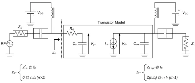
The matching networks are used to present optimal source and load impedances to the active stage, thus ensuring their proper operation. Matching networks in this work are split in unit L-Cells. The number and size of these unit elements can be determined by using bandwidth and insertion loss requirements.
Matching networks can be made reconfigurable using tunable components such as switched capacitors. Therefore, the design of switched capacitor banks taking into account that those components must operate under high power levels is also presented.
Finally, the design of a single pole multiple throw RF switch is introduced in section II-5 since it represents a critical building block of multiband PA design.
36
II-1
Power amplifier characteristics
PA designers have to find optimal trade-off between gain, output power, linearity and efficiency. The Simulated response of linear PA optimized for 3G applications is shown in Figure 22.
Figure 22: Gain, ACPR and power added efficiency performance of a 3G power amplifier II-1.1. Power gain
From Figure 23, the power gain (GP) of the amplifier is the ratio of the output power (Pout) over the input power (Pin) as expressed by Equation 4.
Figure 23: Schematic representation of the power flowing in and out of a power amplifier.
𝐺𝑃=𝑃𝑃𝑜𝑢𝑡
𝑖𝑛 Equation 4
Figure 24 depicts a power amplifier together with its source and load impedances as well as all the different power expressions along the amplifier stage.
PAE Gp
ACPR (up & down) ACPR limit PSS Plin P1dB Psat Amplifier Supply Pin Pout Psupply Pdiss
37
Figure 24: Power amplifier with source and load impedances.
On this schematic, the input power is delivered to the PA by a power source characterized by a RF voltage eg and source impedance Zsource. The amplified output signal is delivered to the load impedance Zload. The transducer gain is the ratio between the output power and the available power from the generator (Equation 5).
𝐺𝑇=𝑃𝑃𝑜𝑢𝑡
𝑎𝑣𝑔𝑒𝑛 Equation 5
In order to avoid reflection at the input of the power amplifier, the source impedance should be matched to the conjugate input impedance of the amplifier. In that case, Pin = Pav gen and GT = GP.
II-1.2. Efficiency
Due to dissipated power Pdiss, only part of the supplied power is contributing to the amplification. Efficiency is a measure of the DC power conversion to RF power. In PA design, we define two different expressions for efficiency. The first is the drain efficiency, which is given by Equation 6.
𝜂=𝑃𝑃𝑜𝑢𝑡
𝑠𝑢𝑝𝑝𝑙𝑦 Equation 6
The power added efficiency (PAE) takes into account the input power as shown in Equation 7. Note that using Equation 8, PAE can also be expressed as a function of η and Gp.
𝑃𝐴𝐸=𝑃𝑜𝑢𝑡𝑃 − 𝑃𝑖𝑛 𝑠𝑢𝑝𝑝𝑙𝑦 Equation 7 𝑃𝐴𝐸= 𝜂 ∙(1 −𝐺1 𝑝) Equation 8 Amplifier Supply Pav amp Pout Pav gen Pin Zsource Zload eg GP GT
38
Using this equation, it becomes clear that the higher Gp, the closer PAE is to η. The objective for the PA designer is to maximize PAE. Efficiency is a critical parameter when comparing different PA design. In this work, when efficiency is mentioned without further indication, it is referring to
PAE.
II-1.3. Linearity
Linearity is another critical parameter which has to be traded-off with efficiency in PA design. A power amplifier is not operating linearly most of the time as large signal operation leads to non linearity.
A. Compression and saturation
Compression and saturation can be observed on the gain characteristic of a power amplifier. Figure 25 shows the output power and power gain as a function of input power.
Figure 25: Output Power (left) and Power Gain (right) versus Input Power of a medium power amplifier.
On this figure, two domains can be distinguished. The first one is the linear zone, for which the gain is constant. Operation in this zone is also called Small Signal operation as the magnitude of RF signal is small enough to ensure linear operation.
The non-linear zone is characterized by variations of gain according to the input power. When the amplifier operates in this zone, gain expansion and/or compression (AM/AM distortion) occurs; as well as phase shift (AM/PM distortion). The 1dB compression point (P1dB or IP1) is the point at which the gain is 1dB lower than the ideal linear gain extrapolation, shown in dotted line on Figure 25.
Under specific conditions, the PA can show gain expansion. On Figure 25, between -5dBm and 10dBm of input power, where the gain is higher than the small signal gain. This condition can be exploited to boost the gain of the power amplifier and therefore increase the P1dB.
Another specific region can be defined inside the non-linear zone and is called saturation zone. In this range, the output power of the PA is saturated at a maximum value (Psat).
B. Inter-modulation
Inter-modulation distortion can be observed by injecting two tones at the input of the PA device and by observing the output spectrum of the PA. Figure 26 shows such response for orders limited to 3.
-1 dB
P1dB P1dB
Gain expansion
Linear Zone Nonlinear Zone
Sa tu ra ti o n Z o n e Psat
Linear Zone Nonlinear Zone
Sa tu ra ti o n Z o n e
39
Figure 26: Illustration of the inter-modulation distortion of a power amplifier.
As can be seen on the figure, the 3rd order inter-modulation distortion (IMD
3) products are close to the fundamental frequencies. Considering the two fundamentals represent the desired signal bandwidth, or channel, IMD3 represents signal leakage in adjacent channels. Therefore, IMD3
constitute another criterion to quantify non-linearity of a PA device. Figure 27 shows a schematization of IMD3 quantification.
Figure 27: Two tone PA response showing 3rd Order Inter-Modulation Distortion
The IMD3 “up” is the difference between the higher tone and the higher IMD3, see Equation 9. Equivalently, the same definition can be given for the IMD3, “down”, see Equation 10.
𝐼𝑀𝐷3𝑢𝑝[𝑑𝐵𝑐]= 𝑃(2𝑓2− 𝑓1)[𝑑𝐵𝑚]− 𝑃(𝑓2)[𝑑𝐵𝑚] Equation 9 Amplifier Supply Input Output |Pout|(f) f f1 f2 2f1 2f2 3f1 3f2 Harmonics 2nd 3rd Intermodulation Products 2nd 3rd f2-f1 f2+f1 2f2-f1 2f1-f2 2f1+f2 2f2+f1 |Pin|(f) f f1 f2
![Figure 5: Reconfigurable multimode PA with transistor sizing and reconfigurable matching network [Kang13]](https://thumb-eu.123doks.com/thumbv2/123doknet/12856191.368244/18.892.116.792.101.364/figure-reconfigurable-multimode-transistor-sizing-reconfigurable-matching-network.webp)