j
Design and Simulation of a 20 Gbps Communication Channel
by Abigail C. Rice
S.B. Electrical Science & Engineering
Massachusetts Institute of Technology, 2014
MASSACHUSETTS INSTITUTE
QF TECHNOLOGY
.AUG 20 2015
LIBRARIES
ARCHIVES
Submitted to the Department of Electrical Engineering and Computer Science
in Partial Fulfillment of the Requirements for the Degree of
Master of Engineering in Electrical Engineering and Computer Science
At the
Massachusetts Institute of Technology
May 2015
C
VNe- 2o
I5
All rights reserved.
Author:
Department of Electrical Engineering and Computer Science
Certified by:.
1
0
U
Alan Pfeifer Manger, Hardware Engineering, NetApp Inc. VI-A Company Thesis SupervisorCertified by:.
Luca Daniel Emanuel E. Landsman Associate Professor of Electrical Engineering MIT Thesis Supervisor
A A
Accepted by:
Prof. Albert R. Meyer Chairman, Masters of Engineering Thesis Committee
MITLibraries
77 Massachusetts Avenue
Cambridge, MA 02139 http://Iibraries.mit.edu/ask
DISCLAIMER NOTICE
Due to the condition of the original material, there are unavoidable flaws in this reproduction. We have made every effort possible to provide you with the best copy available.
Thank you.
The following pages were not included in the original document submitted to the MIT Libraries. This is the most complete copy available.
p.113
Design and Simulation of a 20 Gbps Communication Channel
By
Abigail Rice
Submitted to the
Department of Electrical Engineering and Computer Science
May 22, 2015
In Partial Fulfillment of the Requirements of the Degree of
Master of Engineering in Electrical Engineering
Abstract
Digital wire-line communication speeds are increasing rapidly to achieve ever higher data rates. Speeds beyond 20Gpbs are desirable for the next generation of protocols. However, higher frequency signals experience more loss due to the physical channel and are more sensitive to small imperfections in the channel, such as vias. In this work, an existing communication
channel between two controller boards across a midplane was improved to allow for operation at a higher frequency. Mentor Graphics HyperLynx was used to simulate the channel and display S-parameter models and eye diagrams to demonstrate the impact of various designs. The effects of the material properties, impedance of the traces, and vias were simulated and the results combined to determine what physical layer improvements must be made to reduce loss and reflections at this high frequency.
MIT Thesis Supervisor: Luca Daniel
Associate Professor, Department of Electrical Engineering and Computer Science Company Thesis Supervisor: Alan Pfeifer
Acknowledgement
My sincere thanks to Alan Rymph, my VI-A company advisor for teaching me signal
integrity and being a great mentor throughout the research process. Your guidance shaped so much of this thesis and how I approach research.
I would also like to thank Alan Pfeifer, David Hyde, and Robert Stubbs at NetApp for
answering my questions and guiding me on choosing a topic. I would also like to thank Steve Miller, Senior Technical Director at NetApp for his continual support.
Last but not least thank you to my MIT faculty supervisor, Prof. Luca Daniel for being willing to supervise my thesis and for introducing me to signal integrity theory.
Table of Contents
Page Abstract... 2 A cknowledgem ent ... 3 Table of Contents... 4 List of Figures ... 7 List of Tables ... 7 1 Introduction... 81.1 M otivation and Problem Statem ent... 8
1.2 Objective ... 9
2 Theoretical Basis... 9
2.1 Differential Transm ission Line Theory... 10
2.1.1 Im pedance of a transm ission line... 10
2.1.2 Capacitance ... 11
2.1.3 Inductance ... 11
2.1.4 Calculating D ifferential Im pedance ... 12
2.1.5 Reflection... 12
2.2 Printed Circuit Board D esign ... 14
2.2.1 Conductive Copper Layers ... 15
2.2.2 Insulating Dielectric Layers... 16
2.3 Via D esign... 17
2.3.1 Anatom y of a Via... 17
2.3.2 Im pedance of a Via... 19
2.4 Electrical Properties of M aterials... 19
2.4.1 Dielectric constant ... 19
2.4.2 D issipation factor ... 21
2.4.3 Frequency dependence of D f and Dk... 23
2.5 Attenuation of the signal ... 24
2.5.1 Resistive loss comes from the inherent resistivity of copper... 26
2.5.2 Dielectric loss comes from the absorption of the surrounding dielectrics... 28
2.6 M easuring Signal Quality... 29
2.6.1 Frequency D om ain - S-Param eters ... 30
2.6.2 Tim e D om ain- Eye Diagram s ... 33
3.1 Path Design ... 34
3.2 Schem atic Creation ... 35
3.2.1 SPICE Driver M odels ... 35
3.2.2 PCB Trace M odels ... 36
3.2.3 Via M odeling ... 36
3.2.4 Connector M odels... 36
3.3 Sim ulation Approach... 37
3.4 Resources ... 38
3.4.1 M entor Graphics HyperLynx ... 38
3.4.2 Inform ation Resources ... 38
4 Results ... 38
4.1 Dielectric M aterial... 38
4.1.1 W hat is a better m aterial? ... ... ... ... . . 39
4.1.2 Dielectric Constant affects the im pedance of the traces ... 40
4.1.3 Effects of the M aterial on Loss ... 41
4.1.4 M aterial Choices ... 43
4.1.5 Effects of the Material on the Maximum Length of the Trace ... 49
4.1.6 Effects of the M aterial on the Vias ... 51
4.1.7 Controller Via Im pedance... 53
4.1.8 Controller Via Insertion Loss... 56
4.1.9 Com parison to the M idplane Vias ... 58
4.1.10 Com bined Effects of the M aterial on the Full Path ... 59
4.2 Resistive loss ... 65
4.2.1 Effects of Geom etry on Differential Im pedance... 66
4.2.2 Effects on Resistive Loss -Bigger is Better... 68
4.2.3 Varying Two Factors to keep the Impedance Constant ... 71
4.2.4 Separation to W idth Ratio... 73
4.2.5 Im pact on the Full Schem atic ... 73
4.3 Im pedance Control ... 76
4.3.1 Effect of an im pedance discontinuity ... 77
4.3.2 M ultiple Discontinuities... 78
4.3.3 Controller Im pedance Tolerance... 82
4.3.4 Full Path Impedance Tolerance ... 87
4.4 Via design... 89
4.4.1 Stub Length... 90
4.4.2 V ia Drill Size and Spacing... 92
4.4.3 V ia Pad Size... 94
4.4.4 V ia A ntipad Size... 96
4.4.5 Return V ias ... 97
4.4.6 For an impedance of 100 Ohms, what gives the lowest loss? ... . ... ... . . . 99
5 Conclusion and Future W ork... 104
6 References... 106
7 Appendix... 107
List of Figures
Page
Figure 1 A diagram of a sample PCB stack up ... 15
Figure 2 Alignment of the dipoles in a dielectric material with the electric field. ... 20
Figure 3 The signal velocity is proportional to 1/4Dk and the time delay is the inverse ... 21
Figure 4 Frequency dependence of the real and imaginary parts of the dielectric constant... 24
Figure 5 Circuit model of one section of lossy transmission line... 25
Figure 6 Attenuation of the signal per inch. ... 26
Figure 7 Diagram of a cross- section of an inner differential pair... 27
Figure 8 Dielectric loss from the dielectric constant ... 29
Figure 9 The Dielectric Constant affects the single-ended impedance of the trace as l/Dk... 40
Figure 10 The trace width can be increased to compensate for a lower dielectric constant... 41
Figure 11 Simulated dielectric loss for dielectric constant and dissipation factor. ... 42
Figure 12 Effects of the material properties on the total loss. ... 43
Figure 13 The attenuation per inch of a stripline trace using various materials ... 45
Figure 14 Loss graphed against the dielectric constant and the dissipation factor... 45
Figure 15 Effect of the dielectric constant and dissipation factor. ... 48
Figure 16 Eye Diagram collapse for selected materials... 49
Figure 17 Insertion loss over different lengths for the selected materials. ... 50
Figure 18 Impedance of the vias using the TDR simulator. ... 54
Figure 19 Effects of the material on the Via impedance. ... 55
Figure 20 Via Entry impedance increases with lower Dk. ... 56
Figure 21 Via differential insertion loss for selected materials. ... 57
Figure 22 Effects on the m idplane vias... 59
Figure 23 Insertion loss of the full path ... 61
Figure 24 Return Loss data for the full path schematic... 62
Figure 25 Eye D iagram for the full path. ... 63
Figure 26 Eye Diagrams for IS415, EM888, and MegTron7. ... 64
Figure 27 Rise time of the signal through the full path. ... 65
List of Tables
Page Table I Matrix of standard and mixed-mode S-Parameters. ... 32Table 3 Summary of the materials investigated... 44
Table 4 Maximum length of a trace for a budget of -16 dB. ... 51
Table 5 Rise Time degradation from the material. ... 65
Table 1 Effect of increasing a test variable when compensated by each of the other factors. ... 71
Table 6 Different cases of impedance tolerance investigated. ... 87
1 Introduction
Information technology is advancing at a very fast pace and has been driving faster and faster data speeds. Of the many IO standards in use today, the fastest two used for high-performance data storage are PCIe and SAS. The current systems are generation 3, with PCIe Gen 3 running at 8 Gbps and SAS3 at 12 Gpbs. But as good as these are, the current data rates are still a bottleneck of many systems so even faster systems will be required in the near future. Every generation of these protocols has doubled the data rate, and PCIe Gen 4 is expected by be
16 Gbps and SAS 4 20-24 Gbps. However, higher speed signals have more loss and tighter jitter
constraints due to the skin effect, reflections, and dielectric materials, so current PCB designs will no longer be adequate. Higher quality materials, improved via and trace design, and tight impedance control will all be necessary to enable these higher speeds. The goal of this thesis is to design a higher quality interconnect capable of delivering data at speeds of 16-20 Gbps.
Chapter 1 details the background and motivation for this work, then a review of the
theoretical concepts required for this work is given in chapter 2. Chapter 3 explains the process used to create and analyze the channel. Simulation results are given in chapter 4. Chapter 5 is a discussion of the work and possible future research.
1.1 Motivation and Problem Statement
Current speeds for PCIe Gen 3 go up to 8 Gbps and SAS3 to 12 Gbps. To get a higher amount of data throughput, either many parallel channels must be used or each one must become faster. In the near future, fourth generation protocols will be developed which will seek to double to current data transfer rate. This is accomplished by a mixture of a more efficient encoding scheme and by improvements to the psychical layer allowing for a higher signaling
frequency. At the time of this work, the full specifications for the next generation of SAS 4 and PCIe Gen. 4 have not been created. However, to attain a higher data rate an improved physical channel must be designed. The physical layer is largely independent of the precise timing, encoding, and other specifications of SAS or PCIe. This thesis explores the various challenges associated with higher bandwidth interconnects and suggests improvements for creating a channel running at a bandwidth up to 10GHz, which corresponds to a 20Gbps data rate.
1.2 Objective
The goal of this work is to design a physical interconnect with a bandwidth of 10GHz and an acceptable amount of loss and reflections. The channel is between two controller boards connected by a midplane. Many different aspects of the design affect the performance of the overall interconnect, but for this work three major areas are examined that contribute significantly to signal integrity issues. The focus is on the total loss due to the dielectric material, impedance discontinuities along the path, and the incorporation of vias.
2 Theoretical Basis
This work relies on a detailed knowledge of signal integrity concepts. It is important to understand the essential principles of transmission lines, reflections, loss, and how the PCBs are manufactured.
Signal Integrity refers to the quality of an electrical signal. Information is converted to a voltage signal that is sent down the transmission line. Ideally, it would arrive at the other end of the path exactly as it was sent. However, the signal is distorted by noise, reflections, and losses. Electrical noise is added to the signal from outside sources, which could be nearby signals
(referred to as crosstalk), from the physics of the devices and traces, or from EM waves from outside travelling near the trace and inducing a voltage. Reflections occur when the signal sees some change in the path that causes the wave to bounce around and distort the voltage. Loss occurs from the signal travelling through real materials that absorb some energy and convert it to heat.
This chapter describes the technical background needed for the reader to understand the results of the simulation work. It briefly describes transmission lines, the design of current PCBs, sources of loss, and two of the major methods used to measure signal integrity.
2.1 Differential Transmission Line Theory
Most high-speed signals are transmitted as a differential voltage using a differential transmission line. Differential transmission lines are created with two conductive traces by
applying a complementary voltage (a positive signal and the negative signal). One advantage is that this method will reject most noise, if it is common to both traces. Both lines will experience the same noise, so when one is subtracted from the other, the noise will cancel out. The
complementary line also provides a nearby path for the return current.
2.1.1 Impedance of a transmission line
The impedance of a signal path describes how the signal will respond to, or impede, an incoming signal. Voltages and currents are affected by the resistance, capacitance, and inductance of the connection. Both the AC waveform's magnitude and phase will be affected. Similar to resistance, it is defined as the ratio of the voltage to the current of the signal travelling in a particular direction. This means that the forward voltage is equal to the impedance times the forward current, but the total voltage/current need not be equal to the impedance if there are
reflections and multiple waves. The characteristic impedance of a transmission line is Zo
related to the inductance and capacitance of the line.
2.1.2 Capacitance
The capacitance primarily measures the response of the transmission line to the electric field created by the propagating signal. An electric field is created by the voltage on the conductor and spreads outward towards other conductors. The amount of electric field that the transmission line creates is determined by its geometry and the dielectric constant. Just as in a parallel plate capacitor, the capacitance is proportional to the surface area of the conductors and inversely proportional to the distance between them. This means that increasing the trace width or thickness will increase the capacitance and increasing the separation or the dielectric height will decrease it.
When a transmission line passes through a non-uniform material, such as on the top of a PCB where half is in air and half inside the dielectric of the board, the dielectric constant is an effective dielectric constant that the signal sees in all of the volume it passes through.
2.1.3 Inductance
Inductance primarily measures the response of the transmission line to the magnetic field looping around the conductors. The inductance is defined by the area of the current loop and the magnetic permeability. In PCBs, magnetic materials are rarely used so the relative permeability is 1. The loop area includes the entire path-signal and return-and depends heavily on the height of the dielectric and the proximity of the return path to the signal path. For example, if there is a break in the ground plane beneath a signal, the return current must flow all the way around the gap instead of close under the trace. This increases the inductance of the loop. Impedance
therefore depends on four major geometric factors: the width of the trace, the spacing between traces, the height of the dielectric, and the thickness of the copper trace.
2.1.4 Calculating Differential Impedance
The differential impedance of a trace can be approximated with the equation: Z 120 xln 1.9(2h + t)
-. 9 1-O.374e~ )
SxIn(.8w t
Where:
h=dielectric height in mils (symmetrical)
t = copper thickness in mils
w = trace width in mils
s = separation between traces (mils)
Single ended impedance (SE Zo) is the impedance of one uncoupled trace and the diff Zo refers to the differential impedance of the trace pair.
2.1.5 Reflection
When a signal propagates down an ideal uniform transmission line, it creates exactly the same electric and magnetic fields down the length and the signal arrives at the other side exactly as it was sent. However, if there is a change in impedance, the signal will be distorted. This is because the signal is travelling as a wave that must remain continuous, so no sharp rises or drops are allowed since that would require an infinite electric field. As long as the path is passive, the current must remain constant throughout otherwise there will be a sink or source of charge. But the current and voltage in the line are related by the impedance, so if the impedance on one side is different than the impedance on the other side, the current and voltage must also logically change. This is what creates a reflected wave travelling backward to keep the voltage and current continuous.
The boundary conditions require that the voltage be the same on both sides. This is from Guass's law, V - =
--
,
that the divergence of the electric field is equal to the enclosed charge.When this is taken across a passive boundary (with no net charges built up inside), the total divergence must be zero. This means that the electric field in one direction is equal and opposite the electric field in the other direction. And since E = -VV, when the electric field is zero, the gradient of voltage must also be zero and so the voltages are the same on either side of the boundary. Therefore Vinc + Vrefl = Vt. The current must also be the same across the boundary.
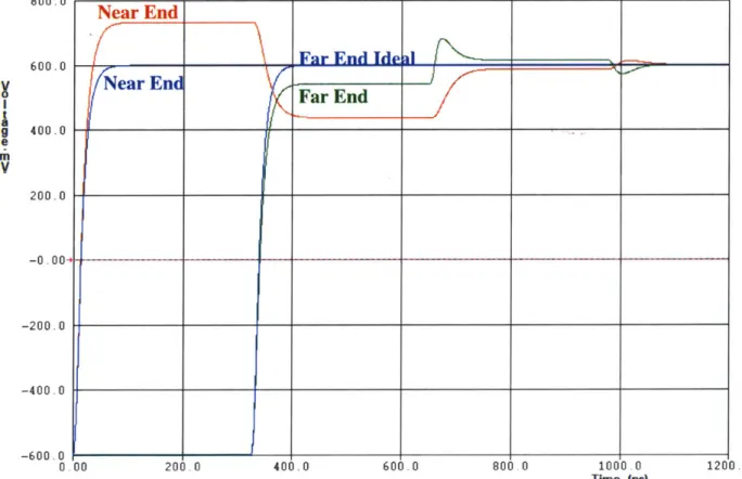
This is because the current is a flow of charge, and charge cannot be built up in a passive structure. These conditions will force a new voltage and current waveform to be created travelling in the opposite direction. One example voltage waveform is given below in figure 1, showing both the near end and far end voltages for an ideal case and a case with a large impedance discontinuity.
Voltage waveforms for an ideal channel and a channel with a large reflection
800 . 0 600 t g 400 e m 200 -0. -200 -400 -600 Near End .0 Fr End Ide Near End .0 .0 00-1 .0 .0 .0
U U 2U ZUU . U 4. UbU.U uu.u .UUU1.U I 2.U
Time (ps)
the near end. The transmitted voltage is reduced until the reflection has time to reflect again off the source impedance and travel back down the channel to the endpoint. Thus the far end does not reach the true voltage until more than three time delays.
Signals get distorted when they encounter a change in impedance. When there is a boundary between two different impedances (such as a change in the cross-section of a trace), some of the signal reflects and some gets transmitted. The ratio of these parts depends on the difference in impedance. Reflected signals travel back down the line in the opposite direction of the original signal. They can either add or subtract from the voltage amplitude. If there are multiple such boundaries, reflections can bounce back and forth and build up. It is therefore important to keep the impedance constant along the entire path, especially at the two ends of the channel called terminations. This will minimize any reflected signal and keep the information in the signal preserved.
2.2 Printed Circuit Board Design
PCBs are made of stacked layers of copper foil in between insulating dielectrics. To create a PCB, first glass fabrics are filled with liquid resins and partially cured. This is often called pre-preg (pre-impregnated). Cores are formed with layers of glass and resin with a copper foil on each side. PCBs are made with alternating core/pre-preg layers such that there is a layer of dielectric insulating nearby copper signal layers. The foil on each side of the cores is etched to create the design of the traces and pads of the board, and then stacked with a pre-preg layer, then another core, and so on. The stack is heated and pressurized to cure.
-- - -- - - -- I TOP GNDI POWERTop Signal2 GND2 SignaI3 GND3 Signal4 Signals GND4 Signal6 GNDS Signal7 POWERBottom GNDE BOTOM Pre-Preg Core Pre-Preg Core Pre-Preg Core Pre-Preg Core Pre-Preg Core Pre-Preg Core Pre-Preg Core Pre-Preg
Figure 2 A diagram of a sample PCB stack up showing the copper layers, insulating layers, and the placement of signal and
plane layers.
2.2.1 Conductive Copper Layers
Copper is the conductive metal most commonly used in circuit boards. Copper foil is formed through electro-deposition or rolling copper to a uniform thickness sheet. The thickness of the sheet is measured by the weight of the foil over a one square foot area. Common weights are 0.5 ounces and 1 ounce (higher weight copper foils are thicker). The thickness of the copper is important for design because it affects the impedance of the trace, the resistance of the trace, and the amount of current the trace can carry. Thicker copper has less resistance (and hence less conductive loss), higher current carrying capacity, but lower characteristic impedance.
There are two main functions of the copper layers: to connect the signals and to provide power and ground connections. Most high speed signals are routed as a differential pair in between two reference planes. The power and ground are delivered by the planes of copper so they have the lowest impedance and highest ability to carry the current. Often, the signal layers are routed with thinner copper than the planes because they do not need to carry as much current. Also thinner copper has better impedance control because it is easier to etch a thin foil more uniformly. The top and bottom layers are necessary to connect the traces to the devices mounted on the surfaces, but these layers are not desirable for high speed routing because there is more cross talk and less control on the width and thickness.
Typically copper foil is treated on the surface to improve the adherence to the resin layers. Small bumps in the copper provide a much better grip for the resin and prevents sliding or delaminating. However, the uneven surface also has more loss. This is because the current traveling on the outer surface has to traverse all the hills and valleys which lengthens the path and increases the resistance. Surface roughness does cause more resistive loss, but it is not considered in this study.
2.2.2 Insulating Dielectric Layers
The dielectric is the insulating material between the copper layers to isolate the signals and provide structural support to the board. Generally these layers are composed of a fiber glass woven cloth impregnated with some type of resin. Glass cloth comes in many different styles for different thicknesses, fiber density, and resin content. Glass often has a high dielectric constant compared to the resin, so the overall dielectric constant of the material is dependent on the percentage of resin in the layer as well as the characteristics of the resin itself.
There are many different types and compositions of resins. Their function is to fill all the space between the layers and provide adhesion between the glass and the copper foil. Electrically, the most important characteristics are the dielectric constant (Dk) and the dissipation factor (Df), which contribute to the impedance and loss of the board. When doing a full design, the mechanical and thermal properties should also be considered, but they are not a part of signal integrity simulations. The dissipation factor is the most critical variable in determining the performance of traces on the board. Df can be correlated with the attenuation per length and thus defines how long the trace can span and still maintain good signal integrity.
2.3 Via Design
Vias are used to connect traces on different layers of the PCB. They often cause signal integrity problems in high speed lines because the impedance of the trace does not match the impedance of the via, which causes reflections. The best way to reduce these reflections is to match the impedance of the via as close to the trace as possible.
Another signal integrity issues with vias is the potential for stubs. Stubs are extra metal connected to the trace so that the signal splits, travels down the stub, reflects of the end, and then mixes with the original signal with a phase delay due to the extra length it had to travel. The worst case is when the stub length is 1/4 the wavelength, so a full trip is half and the phase is exactly out of phase and the two signals cancel. This problem can be avoided by backdrilling the vias to remove these stubs.
2.3.1 Anatomy of a Via
Vias are more complicated structures than the traces. To create a via, the board is first drilled with a small drill bit. Then the hole is plated with copper, leaving a smaller diameter hole. On
AJ
layers where there are traces that must connect, circular rings called pads are used to create a better contact and to ensure the trace will still connect with slight alignment errors. All other layers must not contact the via, so antipads are etched away on the plane layers. A differential via has two barrels running through the board, pads on the layers with connecting traces, and antipads on the other layers.
Figure 3 Via Design. The top view is on the left, looking at the top
of the board with an incoming differential pair connecting to a via pair. The blue represents the ground plane. The diagram on the right is a cross-section of the same via showing the different layers the via passes through. In this case, the via enters on the top layer and exits on signal layer 7, leaving a short stub on the end. Important dimensions have been labeled.
Signal Vi ad * ,rill Si pa proach An Signal Vi Ground Plane
Return Via Signal Via + Signal Via
-I try I
Return Via
Drill Size
N eturn Via Dista'c
Via Spacing Exit La
Sttub Length
Ground Planes "Pads 1ifferential
2.3.2 Impedance of a Via
The impedance of a via is determined by the geometry of the via and the material surrounding the via. The most important parameter is the spacing to drill size ratio (s/D). The other factors affect the excess capacitance the via sees, and are lumped together as Dkeff. This is not simply the Dk of the material, but it also involves the antipad size, the pad size, the number of pads, and the stackup. One approximation for the impedance of a via is:
Z0 =~ ef2 In S+ - 1
t atcm i (, r,1
where SID is the spacing to drill size ratio and Dkeff is the effective dielectric constant
2.4 Electrical Properties of Materials
2.4.1 Dielectric constant
The dielectric constant is a measure of how a material responds to an electric field, also called the permittivity. When an electric field is present, the field exerts a force on the positive and negative charges within the material (ions, polar molecules, and electrons). The molecules line up their charges with the direction of the field, as depicted in Figure 2. Each dipole's small electric field is then added to the external electric field, and the field gets stronger.
Random alignment with no electric field Dipoles aligned with the electric field
Figure 4 Alignment of the dipoles in a dielectric material with the electric field. The flux density increases, the capacitance gets larger, and the signal slows down. The movement of the dipoles causes a small current to flow to the ground plane.
Often, the term "dielectric constant", or Dk, actually refers to the relative permittivity (cr) defined where 1 is the permittivity of a vacuum (Co = 8.85 x 10⁻¹² F/m). Air is very close to this value, but all other materials have a higher dielectric constant because of the presence of charges inside the material. A related factor is the permeability, which defines how the material
responds to magnetic fields. But for most materials, the permeability is the same as the permeability for a vacuum (p. = 471 x 10-7 Vs / Am), so the relative value is treated as 1.
The permittivity and permeability define the speed of light in a material. The speed of light, c, is constant in a vacuum but slows down in media due to the extra interactions of its electric and magnetic fields. One way to explain it is by thinking of the dielectric constant as increasing the capacitance the signal sees down the line. As it propagates, it must charge up all the capacitors distributed in the material which takes longer with larger capacitors. The permittivity of a vacuum is defined as:
C =1
AI
Since magnetic materials are not typically used to: V =
Velocity
0.012 0.01 0.008 0.006 0.004 0.002 0 v = 0.0118 in/ps x Dk-0-0 2 4 6 Dk 8 10 12in PCBs, the speed of signals can be simplified
C/Dk
Time Delay
300 250 5200 .~ 150 100 50 0 0 2 4 6 Dk 8 10 12Figure 5 The signal velocity is proportional to 1/VDk and the time delay is the inverse, VDk. Higher dielectric constants increase the capacitance and slow the propagation of the signal.
2.4.2 Dissipation factor
Dissipation factor is basically a measure of how many dipoles are in the material and how far each of them can move. The dielectric constant describes how the capacitance is increased by the dipoles present. How the dipoles move inside a material is strongly dependent on how they are attached to the polymer backbone and the mechanical resonance. Thus the more cross-linked the polymer is, the less the molecules can move around, and the lower the dissipation factor.
The movement of dipoles causes loss as it converts the electrical energy into mechanical energy and then into heat. This is exactly how a microwave oven works, the electromagnetic wave at 2.45 GHz aligns the water molecules in food, causing them to move back and forth with the field and absorb the electric energy of the field and convert it to heat. In a PCB, the same
0.
0
Z,
mechanism occurs, but the dissipation factor is much lower so only a small part of the energy is lost and very little heat is produced.
Mathematically, Df comes from the complex nature of the dielectric constant. The current through an ideal capacitor is always 900 out of phase with the voltage, I = C dV/dt. When complex number notation is used, the current through a capacitor is purely imaginary, I =
jo>CV, or using the relative dielectric constant. I = jo) r C.V. This describes an ideal, lossless
capacitor between the trace and the reference plane.
However, there is also a loss or leakage current that is flowing in phase through the dielectric from the motion of the dipoles. When the dipoles move back and forth, they create an
AC current in phase with the voltage. This behaves like a resistor, and real current flows across
the dielectric. Both arise because the dielectric constant is actually a complex number, Er = Cr' - j
Er", where Er' is the real part of the constant (Dk) and r" is the imaginary part of the constant.
Using this notation, the current through the lossy capacitor is:
I = jO) CrcoV = jO) (Cr' -
j
Er") CoV = jO)FC'CoV + O)E,"CoVThe imaginary part of the current creates the capacitive effects where the current is out of phase with the voltage and the real part describes the leakage current where the current is in phase. The real part of the dielectric constant, r' or Dk, contributes to the out of phase part (capacitor) and the imaginary part, Cr", contributes to the in phase part (resistor). The leakage resistance is related to the dissipation factor and the frequency. As the frequency increases, the dipoles move the same distance, but faster so the current increases and the conductivity increases.
RLeagage= 1/wDfCL GL= l/RL = W Df CL
The precise definition of the dissipation factor comes from the complex dielectric constant described as a vector in the complex plane. The angle of the vector with the real axis is called the loss angle, 6. The ratio of the imaginary part to the real part, or the tangent of the angle, is called the dissipation factor or loss tangent.
Df = tan(o)=
-Basically, the two factors describe the response of the dipoles to an electric field. The dielectric constant is how much the aligning of the dipoles increases the capacitance and the dissipation factor describes how much movement there is and the amount of loss.
2.4.3 Frequency dependence of Df and Dk
Both the dielectric constant and the dissipation factor are also frequency dependent. In real materials, mechanical limitations mean that the dipoles cannot move the same for all frequencies. Effectively, there is a slight decrease in the angle the dipole rotates through. At
high frequencies, the dipoles do not respond as fast so the dissipation factor is slightly less.
However, in typical materials the frequency dependence is fairly small and can safely be ignored in most simulations.
The dielectric constant is also dependent on the frequency. If the dipoles at high
frequency do not get to the full angle they would at a lower frequency, the alignment of the fields is reduced and the effect on the capacitance is smaller. This means that the dielectric constant also decreases with frequency. The amount of this frequency dependence is based on how tightly the dipoles are held, i.e. the dissipation factor. Molecules that are tightly held will have
less variation with frequency. A loosely held dipole will swing wide at low frequency but will be unable to at high frequency. Therefore Df is an indication of the slope of Dk with frequency.
E=E'+ IE"
E dipolar +
e
atomic electroniciionic
103 106 log 1012 1015
['microwave i infrared [IsS IUV'1
Frequency in Hz
Figure 6 Frequency dependence of the real and imaginary parts of the dielectric constant.
One consequence of the variation of the dielectric constant with frequency is that the signal velocity is also frequency dependent. This implies that the higher frequency parts of the signal will travel faster than the lower frequency components. The signal will spread out over time and length, called dispersion. Dispersion is bad for signal integrity, but the part from the frequency dependence of Dk is often small compared to the dispersion caused by loss - higher frequencies have much greater loss than low frequencies. This creates a longer rise time as the signal propagates.
2.5 Attenuation of the signal
Attenuation is the loss of a signal as it propagates down a medium. If the attenuation is too high, the data cannot be effectively detected and the transmission has failed. Loss is observed as a drop in the voltage from one end of an interconnect to the other, but is really a decrease in
the power of the signal. The ratio of the two powers is often expressed in deciBels, the log of the ratio. Since power is proportional to the square of the voltage, the ratio can also be expressed in terms of the ratio of the voltages from one end to the other.
Ratio(dB) = 10 x log - = 10 X log 1 lOx2log -=201o
-PO
V
0The amount of attenuation of a signal within a PCB can be broken down into two parts, the resistive loss from the conductors and the dielectric loss.
Attenuation comes from a lossy transmission line. The ideal transmission line with only inductance and capacitance does not have any loss, and the signal will remain at the same amplitude all the way down the line (assuming no reflections). However, loss exists in real transmission lines. This is often modeled by adding resistors to the ideal model, showing the resistive loss across the conductor and the dielectric loss across the gap to the return path.
RL LL
GL
T
CL
Figure 7 Circuit model of one section of lossy transmission line. The series resistance RL models the resistive loss of the copper and the shunt conductance GL models the dielectric loss.
36,AtxbnM .1. - -- --- ---- - -- - - -32--- - -- - - - ---2.3 21-- -- - - --- - -- - --- - - --- - - - -2.6-- - - - -2.4-- - - -- --- -- -22 --- -.-2 - - _ -- - -1.8 --- - - - ---- --- - --- - - - - -1.6 - - _ 1.4 - - - -- - - -1.2- -- - - -- --- ---- --- - - - - -0.24- - - - _ 0.01 0.1 1 10 100 MMD
Figure 8 Attenuation of the signal per inch. This graph shows the frequency dependence of both the resistive and dielectric losses. The red line shows the resistive loss from the conductor, the green line is the dielectric loss, and the blue line is the total attenuation (the sum of resistive and dielectric components). For this particular trace, the dielectric loss dominates above 14 GHz.
2.5.1 Resistive loss comes from the inherent resistivity of copper
Copper traces are typically designed to have a consistent cross-sectional geometry down the length to keep the impedance constant and minimize reflections. This cross section defines the trace width, the separation between traces in a differential pair, the height of the dielectric material from the trace to the return plane, and the thickness of the trace itself. All of these factors impact the resistance of the copper trace. The trace width and thickness directly affect the amount of cross-sectional area in which the current has to flow. Larger area has a lower resistance, so using wider traces and thicker copper foil will reduce the resistive loss component.
I
I
Ground Plane 1I
I
Ground Plane 2Figure 9 Diagram of a cross-section of an inner differential pair. Four geometric parameters affect the resistive loss of the trace, unrelated to the material properties.
The current distribution is also affected by the nearby currents. Currents flowing in opposite ways attract each other. In a differential pair, the current flows into one trace and backwards from the other trace and the two ground planes. This means that more current will travel along the bottom of the trace near the return plane and along the inside near the complementary trace in a differential pair. In this way, the dielectric height and the separation affect how the current is distributed, how much of the available copper is used, and thus the resistive loss.
Figure 10 Current distribution in microstrip at 100 MHz.
When high speed signals travel, they want to find the path of least impedance. The signal will travel to
minimize the number of field lines circling around it. Inside the conductor, there are more magnetic field lines closer to the center (more inductance in the middle of a conductor than on the edges). The impedance of
high-frequency signals is dominated by the inductance, so current will distribute to minimize the loop inductance. It will spread out as far as possible from itself and as close as possible to a reverse current, which makes the signal travel
on the surface of the conductor. This is called the "skin effect", and means that faster signals will travel in ever smaller sized areas on the exterior of the copper traces. The skin depth, 6, is dependent on the conductivity of the
metal a, the permeability , and the frequency f. It can be approximated by Equation 2 6 1 1
8 2.1pm 1. At 10 GHz, the skin depth is approximately 0.66 pm (0.026 mils). The
fGHz
skin effect makes the resistive loss increases with the square root of the frequency.
1 Equation 2 6 = 1 S 2.1m f GHz where:
6 is the skin depth in microns
a is the conductivity of the metal in Siemens/m
p is the permeability of the metal pop, in H/m
f
is the sine-wave frequency2.5.2 Dielectric loss comes from the absorption of the surrounding dielectrics.
When a signal propagates down a trace, electric and magnetic fields are created that
travel through the dielectric material surrounding the conductor. The electric field is perpendicular to the conductors and causes the dipoles in the material to line up with the field. The movement of these molecules is like a small current from the trace to the ground plane, causing some of the energy of the signal to be lost. When the field changes rapidly, the molecules swing back and forth and absorb more of the energy of the signal. The amount of energy lost depends on the total charge that is moving, the amount that it moves (how tightly the molecules are bonded in the polymer), and how frequently it moves. The dielectric loss is modeled as a resistor from the trace to the return plane, leaking some current out of the trace. The value of the conductance depends on the material properties, the dissipation factor and the loss tangent, but is completely independent of the geometry. The attenuation per length from the dielectric loss is:
20 log e GLZI ( : adiel = 2 = 10 log e (w Df CL) 2 cCCL 21? x 10 log10 e C at 10 GHz: adiel = 2.312 x 10-9 s x 101 0 Hz x Df
Vbf
= in where:GL = conductance across the dielectric = w Df CL
Z.= characteristic impedance
CL = Capacitance per length co = angular frequency = 27f
Df = dissipation factor
Dk = Dielectric constant
23.12 1 Df V/ffk
in
adiel= attenuation per length from just the dielectric loss
c = speed of light in a vacuum (1.18 x 10¹⁰ in/s)
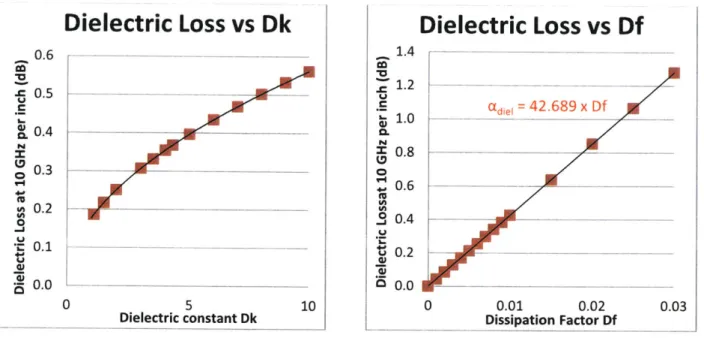
Loss from the Dielectric Constant 0.6 ,
adiel = 23.12*0.008*Dko.5 = 0.18 DkO.5
0 1 2 3 4 5 6 7 8 9 10
Relative dielectric constant Dk
1.4 1.2 V 1.0 0.8 . 0.4 S0.6 0.2 0.0
Loss from the Dissipation Factor
adiel = 2.3*3.70.s*Df =43 Df.
0 0.005 0.01 0.015 0.02
Dissipation factor Df
0.025 0.03
Figure 11 Dielectric loss from the dielectric constant (square root dependence) and dissipation factor (linear dependence) at
10 GHz. In each graph, the other factor is held constant: the dissipation factor at 0.008 and the relative dielectric constant at 3.8 respectively.
2.6 Measuring Signal Quality
There are two basic ways to view the signal: the frequency domain and the time domain. The frequency domain gives information about how the channel responds to various frequencies and the time domain gives information about how the channel responds to a particular data input.
Df xVf5i . C .C0.4 -0.0.3 0 0.2 o 0.1 0.0 n 5
Both views are useful for understanding the causes of signal integrity problems. The frequency domain is generally better at diagnosing the causes of signal integrity problems and the time domain is better suited to determining whether or not the channel is good enough.
2.6.1 Frequency Domain - S-Parameters
The frequency domain gives the response of the channel to sine waves. Since loss and
reflections are both influenced by frequency. the response will change based on the frequency of the sine wave. Scattering parameters (S-parameters) describe how an input sine wave is changed
by the channel. S-parameters are a collection of the scattered responses on each port at every
frequency. Since any signal can be broken down into a bunch of sine waves of various frequencies, this description will completely describe the electrical behavior of any linear, passive system.
S-parameters are defined from the ports they are looking at. Each S-parameter is the ratio of the outgoing sine wave to the incoming sine wave. For example, S21 is the ratio of the
outgoing wave from port 2 to the incoming sine wave on port 1. SI1 is the sine wave coming out
from port I to the incoming sine wave also on port 1. These ratios contain both the magnitude and the phase of the waves (or the real and imaginary parts if using complex number notation).
Every place where a signal enters or exits the device is considered a port. The port impedance is defined to be 50 Ohms. There is no standard numbering, but for this report the ports for a differential channel are numbered with odd to the left and even to the right, as in the following diagram. When this convention is used, S11 describes the reflections from the driver back to itself, and S21 is the transmitted wave down the trace. S1 (and correspondingly S22, S33,
input port. S21 (and S34, etc.) is called the insertion loss, it describes how much signal is
transmitted between the ports when the channel is "inserted" between them. The other parameters describe the crosstalk, S31 is the near-end crosstalk (NEXT), and S41 is the far-end crosstalk (FEXT). These port conventions can be expanded to include more ports, for instance when measuring the effects of multiple trace pairs or a large connector.
10. +2
Port3 Por%4
Figure 12 S-Parameter port numbering. For a differential channel with four ports, 1 and 3 are attached to the driver and 2 and 4 connect to the receiver. Thus S21 refers to the insertion loss between ports 2 and 1 and S1 is the return loss.
When describing a differential pair, the standard S-parameters can be converted to mixed-mode S-parameters. These describe the signal in terms of the differential component and the common component. This is helpful when looking at differential signals since the behavior of the pair as a whole is describes, not just the individual halves. Mixed Mode S-parameters show how the differential signal and common signal respond, as well as how much of one type is converted to another (chiefly by asymmetries between the two traces). Mixed-Mode S-parameters (Sm) can be obtained from the standard S-S-parameters (S,) using a simple matrix conversion, given in Equation 3.
1 0 -1 0]
Smm=M-ISM M 0 1 0 -1 Equation 3
Sr2 5 1 0 1 0
AI
\%A -.--- ..- SDD (2, 1) -- *.---+
SdD O(, 1) SCD (2, 1) SDC(21) sDDj2,2) Mode
4A A '
-SDD (1, 2)!...
-Differential Mod ifferential Mode soc (1 1 .-*.' sc 2 2)
Potl PoRt2
Port 1 Port3 P0r44 Port 2 Com-o-n -SCC (2, 1)'". 'V'- Co.,MM scC('li) .-- --. . 2 2) scc2.2) MOde
scD(12) sC(12 Pont2 Common Mode Common Mode P--ortC 1,)"
Figure 13 Mixed mode port definition.
The S-parameter matrix is always square (n x n with n ports). Below are the matrices for standard and mixed- mode S-parameters, along with their interpretations. The red diagonal is the return loss for each port. The blue elements are the insertion loss. Green represents standard S-parameters' cross-talk between the traces and mixed-mode includes the mode conversion. This thesis focuses on SDDII and SDD21 (differential return and insertion loss), but all of the parameters help to give insight on the behavior of the channel.
Stimulus Port 1 2 3 4 1 SII S12 S13 S14 2 S21 S22 S23 S24 3 S31 S32 S33 S32 4 S41 S42 S43 S44
Table 1 Matrix of standard and mixed-mode S-Parameters.
0 W 1 SDD SDDi _ Differential to -Differential D2 I2 SDCi SDCi Common to -Differential 2 1 2 - U m9~ ,- I -SCD SCD Differential to __ 4 Common D2 1 2 SCCI SCCI Common to Common 2 1 2 __________ - I - i - a - I -Stimulus Port 1 2 3 4
2.6.2 Time Domain-Eye Diagrams
Eye diagrams are used to view the voltage in the time domain. This shows the response of the channel to a random set of bits, not a pure sine wave, typically a worst case pseudo-random bit stream (PRBS). The voltage at the receiver is sensed over a long period of time, and then all of the bit cycles are overlaid. The height of the eye represents the voltage difference between a logic "high" and a logic "low". There needs to be a gap between these two levels so that the receiver can accurately decode the signal. The eye diagram collapses as the loss increases as the voltage amplitude of the sine wave decreases. The width of the eye represents the amount of time during which the signal can be detected. The width can be given in picoseconds, but is more often expressed as a faction of the unit interval (UI) to standardize for different frequencies. The width shrinks because of jitter and reflections. Also, loss lengthens the rise time of the signal which shrinks the width and collapses the eye. A sample eye diagram is pictured below. The color represents the bit error rate (BER) at that location, indicating the density of lines.
To determine if a particular channel meets the specifications, an eye mask is created. This marks a region as forbidden - no lines may enter anywhere in that region. This ensures that the bit error rate will be below a certain level (often 10-12 for PCIe and 10-9 for SAS). This gives a simple pass/fail test for a channel to tell if the signal integrity is good enough that the channel will work. The size of the mask is based on the sensitivity of the receiver. It is defined as a minimum eye height (measured within 0.1 UI of the center) and a minimum eye width (measured at the zero crossing). The eye mask that I used for this paper is displayed below.
<- MaxHeight i O.1U 4
- +9 mV,
Eye Height: 18mV
-0.15 UI +0.15 UI
Eye Width: 0.3 U
Figure 14 Sample Eye diagram and Eye mask.
3 Technical Approach
To determine the impact of the various design choices, a representative controller-to controller path was created and simulated at a frequency of 10GHz. Details of the schematic creation process and simulation are given below. The goal set for the design was a total insertion loss of less than -28 dB, and an eye opening larger than the mask (height greater than 18mV and width greater than 0.3UI).
3.1 Path Design
The controller-to-controller path represents the longest (worst case) path in the system. The channel goes from the TX output across a 6-in long trace on the controller board to a connector which is plugged into the midplane. The midplane is also 6 inches long, then the line passes through another connector back across the controller to the RX pin. The total length of the channel is 18 inches and requires 2 connectors and 6 vias.
3.2 Schematic Creation
I created the schematic using Mentor Graphics Hyperlynx and SPICE models for the driver and receiver. The following is a list of each component and the type of model used in the full circuit. The full schematic is given in Appendix B for reference.
Transmitter buffer SPICE Model
Microstip breakout from package HyperLYnx transmission line
Via S-parameter Via model
Controller routing HyperLynx transmission line
Via S-parameter Via model
Connector External Vendor S-parameter model
Via S-parameter Via model
Midplane routing HyperLynx transmission line
Via S-parameter Via model
Connector External Vendor S-parameter model
Via S-parameter Via model
Controller routing HyperLynx transmission line
Via S-parameter Via model
AC coupling capacitor Ideal 1 OnF capacitor
Microstrip to receiver package HyperLynx transmission line
Receiver buffer SPICE model
3.2.1 SPICE Driver Models
The driver and receiver components were modeled with a simple SPICE circuit. The driver circuit is an ideal stimulus and an RC circuit to set the rise time of the signal. The resistance had to be 50 in order to match the impedance of the PCB traces, and the capacitance was adjusted to create a rise time of l7ps. The receiver is simply a load resistor of 50Q. These
SPICE models are idealized versions of the actual integrated circuits and they ignore the parasitic
effects of the packaging, but they provide a convenient way to compare the physical interconnects when more detailed models are unavailable.
3.2.2 PCB Trace Models
The PCB traces were modeled as transmission lines with a constant cross sectional area and material properties. All traces were differential stripline or microstip. HyperLynx has a 2-D field solver that calculates the impedance of a trace given the geometry and dielectric constant. A sample stackup was created to simulate the structure of the overall PCB. This was a simplified version of a typical multi-layer PCB. Diagrams of the stackup for the controller and midplane are also given in Appendix B. Given the stackup and the geometry of the trace, HyperLynx solves for the impedance and loss resulting from the conductors and dielectric. This way, it was possible to quickly determine the effect of changing the properties of the trace itself (for instance trace width or dielectric constant). Many different combinations were tested and the results complied in the following chapter.
3.2.3 Via Modeling
Vias are necessary to connect different layers of the PCB, but as they are complex 3 dimensional structures they are not as easy to model as transmission lines. To model the vias, HyperLynx's 3-D field solver tool was used. This tool takes the input geometry and PCB stackup information and creates an S-parameter model that describes the behavior of the via across a broad frequency range. These behavioral models take a fairly long time to initially create, but once calculated for a specific via they can fully describe the behavior with a fast simulation time.
3.2.4 Connector Models
The connectors that go between the controller boards and the midplane were simulated with models provided by the manufacturer. Originally, several different connectors from a few vendors were considered. After comparing the different options, the Xcede-HD connector from
Amphenol was chosen due to its loss characteristics at 10GHz. The models were provided as S-parameter files for each pin. For this work, the worst case pin was chosen to ensure the design would work, but in a practical design the high-speed lines could be routed only on the lower loss paths and the worst loss pin could have a lower speed signal on it. The large model was
condensed to a single 4-port S-parameter model which was added to the HyperLynx schematic.
3.3 Simulation Approach
Simulations are highly effective in this type of work because they can provide fairly accurate results without the time and money required to build many different PCB boards and test them. First, the effects of each parameter were explored individually. Then multiple effects were considered in order to design a workable channel. As with any design, there are many tradeoffs present that can be adjusted to fit the particular needs of an implementation. In this work, the impact of the design choices is given to gain a fuller understanding of the behavior of an interconnect at higher speeds so that these choices can be made optimally.
To characterize the design, the behavior of the full channel was analyzed in both the frequency and the time domain. HyperLynx was used to solve for the S-parameters (including the total insertion and return loss). S-parameters make it easy to see the loss of the channel and visualize any resonant behavior due to reflections. The channel was also characterized in the time domain by creating an eye diagram. A pseudo-random bit stream (PRBS) was given to the driver stimulus and the voltage waveform at the receiver was sampled. The eye diagram gave clearer insight on the timing jitter, voltage degradation, and rise time of the signal, and gave an objective comparison against the eye mask that was created earlier.
3.4 Resources
3.4.1 Mentor Graphics HyperLynx
All of the simulations were completed using Mentor Graphics HyperLynx. Both the 2-D
solver and the 3-D via solver were used. HyperLynx has a built-in S-parameter extractor and eye diagram wizard that were used to analyze the channel. All graphs below were created directly from HyperLynx or graphing the output data in Microsoft Excel.
3.4.2 Information Resources
An in depth knowledge of signal integrity was required for this project, which was found
by reading many books and articles listed in the references. These included modeling
techniques, the physics of transmission lines, material properties of PCBs, etc.
4 Results
4.1 Dielectric Material
In this investigation, I wanted to determine the impacts the dielectric constant and the dissipation factor have on the signal. I am focusing on the effects on the impedance and the loss, and then using an eye diagram to see the overall effect on performance. Because there are so many other factors that impact the impedance, the loss, and the overall performance, I aimed to hold the differential impedance from the conductor geometry constant.
I used HyperLynx to simulate designs with various materials, to gain an intuitive understanding of the impact the material has on the signal and to determine the effects on my schematic. All of the loss data, S-parameters, and eye diagrams are at a frequency of 10 GHz (for the eye diagrams this is 20 Gbps, 10 GHz base frequency). First I modeled a simple stripline
trace segment with a transmission line and used HyperLynx's 2-D field solver to calculate the impedance and the loss. The trace was one inch long so that all the loss values would be normalized per inch length. Then I simulated vias using HyperLynx 3-D field solver. I used a consistent geometry based on the dimensions for the Xcede connector via to show the effect from the Dk and Df. Finally, I combined these simulations to the full path schematic I have created to model a controller to controller path. Results are compared in both the frequency domain and the time domain.
4.1.1 What is a better material?
A better material (electrically speaking) has a low dielectric constant and a low loss
tangent. These two factors will decrease the dielectric loss so more of the signal will arrive at the receiver. Such materials enable higher frequency signals and/or longer path lengths with the same amount of loss. Unfortunately, high performance materials also tend to be much more expensive so the options must be considered for how much loss is tolerable for the signal to still be readable with a reasonable bit error rate.
There are many choices available for materials with a range of dielectric constants and loss tangents. The dissipation factor has the biggest influence on the signal attenuation, and the loss is linearly dependent on the dissipation factor whereas it depends on the square root of the dielectric constant. Also, when choosing a dielectric constant, both the loss and the effects on the impedance must be considered. The dielectric material affects the trace impedance by
aig eapaitane. -w-# Dk valu CS HInCreas teII 1111pedalce wIhich necus to Ue
4.1.2 Dielectric Constant affects the impedance of the traces
First, the dielectric constant impacts the impedance because it changes the capacitance
between the trace and the return plane beneath it. Higher dielectric constants will increase the
capacitance which will decrease the characteristic impedance, since Z0 = . Increased
impedance will directly increase the dielectric loss and cause reflections when there is a change in impedance. -Single Ended Zo
Impedance vs Dk
- Differential Zo 200 180 160 -f 1 f E 0120 100 S80 CL E 60 40 20 0 SE Zo = 101.17 0 1 2 3 4 5 6 7 8 9 10relative dielectric constant
Figure 15 The Dielectric Constant affects the single-ended impedance of the trace as 1-Viik
To compensate for the increased impedance, the traces can be made wider, spaced farther apart, raised higher above the return plane, or be made with thicker copper foil. Figure 10 demonstrates widening the trace to keep the impedance at 100 Ohms. This method will reduce the resistive loss, but this is a secondary effect and is not directly related to the material used. When this method is used, the resistive loss will decrease linearly with Dk and the dielectric loss will still decrease as the square root. Alternatively, the width could be increased and the