HAL Id: cea-01376419
https://hal-cea.archives-ouvertes.fr/cea-01376419
Submitted on 4 Oct 2016
HAL is a multi-disciplinary open access
archive for the deposit and dissemination of
sci-entific research documents, whether they are
pub-lished or not. The documents may come from
teaching and research institutions in France or
abroad, or from public or private research centers.
L’archive ouverte pluridisciplinaire HAL, est
destinée au dépôt et à la diffusion de documents
scientifiques de niveau recherche, publiés ou non,
émanant des établissements d’enseignement et de
recherche français ou étrangers, des laboratoires
publics ou privés.
Electroluminescence from a polythiophene molecular
wire suspended in a plasmonic scanning tunneling
microscope junction
Gaël Reecht, Fabrice Scheurer, Virginie Speisser, Yannick J. Dappe, Fabrice
Mathevet, Guillaume Schull
To cite this version:
Gaël Reecht, Fabrice Scheurer, Virginie Speisser, Yannick J. Dappe, Fabrice Mathevet, et al..
Elec-troluminescence from a polythiophene molecular wire suspended in a plasmonic scanning tunneling
microscope junction. Physical Review Letters, American Physical Society, 2014, 112 (4), pp.47403.
�10.1103/PhysRevLett.112.047403�. �cea-01376419�
arXiv:1401.2322v1 [cond-mat.mes-hall] 10 Jan 2014
scanning tunneling microscope junction.
Ga¨el Reecht1 , Fabrice Scheurer1 , Virginie Speisser1 , Yannick J. Dappe2 , Fabrice Mathevet3 , Guillaume Schull1 ∗ 1
Institut de Physique et Chimie des Mat´eriaux de Strasbourg, UMR 7504 (CNRS – Universit´e de Strasbourg), 67034 Strasbourg, France
2
SPEC (CNRS URA2464), SPCSI, IRAMIS, CEA Saclay, 91191 Gif-Sur-Yvette, France
3
Laboratoire de Chimie des Polym`eres, UMR 7610 (CNRS – Universit´e Pierre et Marie Curie), 75252 Paris, France (Dated: January 13, 2014)
The electroluminescence of a polythiophene wire suspended between two metallic electrodes is probed using a scanning tunneling microscope. Under positive sample voltage, the spectral and voltage dependencies of the emitted light are consistent with the fluorescence of the wire junction mediated by localized plasmons. This emission is strongly attenuated for the opposite polarity. Both emission mechanism and polarity dependence are similar to what occurs in organic light emitting diodes (OLED) but at the level of a single molecular wire.
PACS numbers: 73.63.Rt,73.61.Ph,78.60.Fi,68.37.Ef
Controlling the luminescence of a single molecule di-rectly bridging metallic electrodes is a challenging key is-sue towards molecular optoelectronics [1]. Recent exper-iments based on non-imaging methods have shown that the electroluminescence of complex molecular-nanotube [2] and metallic nano-cluster [3] junctions can be excited. Reaching a deeper understanding of these mechanisms re-quires atomic scale control of the geometrical parameters of the molecular junction while simultaneously monitor-ing electronic and optical characteristics [4]. In a pio-neering experiment [5], a scanning tunnelling microscope (STM) was used to excite with atomic-scale accuracy the fluorescence of a single molecule separated from the electrodes by thin insulating layers. While such a weak electrode-molecule coupling is highly favourable for the observation of molecular fluorescence [5–9], a direct con-nectionto the metallic leads is desirable towards integra-tion into molecular scale circuits. To this end, the light emission from atomic [10, 11] and molecular contacts [12] was recently probed, revealing the influence of the cur-rent shot noise at elevated conductances. In such highly coupled cases, however, luminescence mechanisms intrin-sic to the molecule are quenched because of the strong hybridization with the electrode states [13–15].
Here we use the tip of a scanning tunnelling micro-scope to controllably lift a unique π-conjugated polymer chain from a Au(111) surface [16]. In this configuration, both extremities of the π-conjugated wire are directly connected to the electrodes, whereas a long part of the polymer chain is suspended in the junction. Under pos-itive sample bias, light is emitted at the wire junction. Optical spectra reveal a broad resonance whose maxi-mum does not shift with voltage. Based on a simple model, and in agreement with predictions [17, 18], this emission is traced back to the recombination of electrons injected from the tip in the lowest unoccupied molecu-lar orbital (LUMO) with holes injected from the
sam-ple in the highest occupied molecular orbital (HOMO) of the wire junction, showing that direct molecule–electrode coupling and fluorescence can be associated in a single molecular junction. For the opposite polarity, the photon intensity is strongly reduced (quantum yield attenuated by a factor 103
). Our model suggests that this behaviour is due to the non-centred HOMO–LUMO gap respec-tively to the Fermi level of the electrodes at zero voltage, and from the slight asymmetry between the wire/tip and wire/substrate coupling strength. Both emission mecha-nism and polarity dependence are consistent with the be-haviour of a single polymer light emitting diode. Finally, surface plasmons localised at the tip-sample cavity, which are known to amplify inelastic electronic transitions in noble metal STM junctions [15], reveal some unexpected interactions with the wire optoelectronic properties.
The experiments were performed with an Omicron STM operating at 4.6 K in ultrahigh vacuum. The setup was adapted to light emission measurements following the design developed in [19]. In this setup a lens (f-number = 1.5) is fixed to the STM head so that the tip-sample junction can be precisely located at the lens focal point. The collimated light is redirected through an optical viewport outside of the vacuum chamber and is refocused on an optical fibre bundle. The fibre bundle is connected to a detection unit composed of a grating spec-trograph (Princeton Instruments Acton Series SP-2300i) and a liquid nitrogen cooled CCD camera (Princeton in-struments PyLoN-100BR-eXcelon). An overall 1.5% de-tection efficiency is estimated at 500 nm. Au(111) sam-ples and etched W tips were sputtered with argon ions and annealed. To increase their plasmonic response, the STM-tips were covered with gold by micrometer-scale indentations into the sample. The on-surface synthesis of polythiophene nanowires is detailed in [20]. Differen-tial conductance spectra were acquired for a fixed tip-sample distance using lock-in detection (RMS amplitude
2 a b c d e S n
FIG. 1. (a) STM image (9.0 × 10.8 nm2
, I = 2 nA, V = 0.1 V) of a polythiophene wire (inset) polymerized on a Au(111) sample. (b) Normalized conductance G/G0vs tip-sample
dis-tance z for a polythiophene wire suspended in the junction for different voltages. The black curve corresponds to the initial approach of the clean STM tip to a wire extremity. The point of contact defines the origin of the abscissa. (c) Conductance dI/dV spectra (lines) acquired at different tip–sample dis-tances and inverse decay length β (circles) as a function of V , for a given suspended wire. The spectra acquired at z = 4 nm and z = 3 nm are offseted by 3 and 6 nS respectively. (d) Light emission efficiency (squares) as a function of V . (e) Artistic view of a fluorescent polythiophene junction.
= 10 mV, modulation frequency = 740 Hz).
We start by discussing the procedure used to suspend an individual polythiophene wire (Fig. 1a) in the junc-tion. The STM tip is first located atop one extremity of the polymer deposited on a Au(111) surface [20], then approached to the wire up to the formation of a con-tact, and retracted to its initial position while constantly recording the current traversing the junction. The suc-cess of the procedure is attested by the substantially changed slope upon retraction (Fig. 1b). Periodic cur-rent ”jumps” occuring during the lifting procedure are associated to the successive detachments of thiophene units from the surface. Despite these abrupt conduc-tance changes the overall conducconduc-tance traces can be fit-ted as G(z) ∝ Gcexp(−βz), where Gc is the conductance
at contact, z is the tip–sample distance, and β reflects the ability of the wire to transport current [21]. For a sample voltage V = 0.1 V, we find β = 0.40 ± 0.08 ˚
A−1, in good agreement with predictions [22]. At higher
voltages a lowering of β is observed (Fig. 1b). dI/dV spectra recorded for different suspended polymer lengths (Fig. 1c) reveal a first resonance at V ≈ -0.8 V,
an-b a P hot on in tensit y
FIG. 2. (a) Raw and (b) plasmon–corrected spectra of the light emitted by a polythiophene wire suspended in the STM junction for different voltages (1 nA < I < 5 nA). To prevent damages to the wire due to an increased current at elevated voltages, the spectra were acquired at z = 3 nm (V = 1.4 V and V = 1.6 V), z = 4 nm (V = 1.8 V and V = 1.9 V) and z = 5 nm (V = 2 V and V = 2.2 V). The corresponding plasmon amplification function Γ (hν) is shown (dots) in (a). The spectrum at V = 1.4 V was scaled by a factor 5 in (a). As expected for electroluminescent processes [10], the energy of the photons does not exceed the energy of the electrons (hν < eV ), explaining the cut-off (vertical dashes) at the high-energy edge of the spectra.
other at ≈ 1.25 V which progressively disappears when the tip is retracted because of the weaker current (see also supplementary section S1 [23]), and a more intense resonance around 2 V. At this stage it is impossible to assign a LUMO or HOMO origin to these resonances. In-deed, both extremities of the wire are directly coupled to the electrodes (Fig. 1e) and the voltage partially drops at each interface (assuming no voltage drop along the wire itself [24]) causing a displacement of the HOMO and LUMO states in the dI/dV spectra respectively to their positions at V = 0. As reported for graphene nanorib-bons [21], we can see that the reduction of β with V oc-curs when the voltage reaches a dI/dV resonance (dots in Fig. 1c). This effect results from the cross-over from non-resonant to resonant transport regime [21, 25].
We now turn to the electroluminescent properties of the suspended polymer. In figure 2a we display optical spectra acquired at different voltages for the molecular wire probed in Fig. 1c. For V = 1.4 eV, the quan-tum yield of the emission process is in the order of 10−7photon/electron and gradually rises to ≈ 10−5 at
higher voltage (Fig. 1d) due to the larger emission band-width. For the opposite polarity (V = -1.4 V and V = -1.6 V) and the same tip-sample distances, an extremely weak emission (≈ 10−9photon/electron) is detected. As
demonstrated below, this strong variation of the emission efficiency with polarity indicates that the wire states are involved in the luminescence process.
In STM-induced light emission from noble metal elec-trodes, plasmons localized at the tip-sample junction [15] strongly amplify any radiative transition. The energy
dependence of this amplification (Γ (hν) in Fig. 2a) can be deduced from optical spectra of the pristine junction (supplementary section S2 [23]). Assuming that Γ (hν) does not significantly change with tip-sample distance (see supplementary section S3 [23]), the impact of the plasmons on the shape of the spectra can be corrected by normalizing each spectrum by Γ (hν) [26]. For the polythiophene junctions, the corrected spectra (Fig. 2b) reveal the progressive apparition with voltage of a broad resonance centred at 1.8 eV. Interestingly, this resonance does not shift with voltage for V > 2 V. Mechanisms where electrons decay from the wire states directly to states of the electrodes, or vice versa, cannot account for this observation (see supplementary section S4 [23]). This observation rather suggests an emission associated to electrons decaying from one molecular state to another [5]. To confirm this assertion we build up a two Gaussian level model whose parameters at V = 0, given in figure 3a, are justified below. In figure 3b and c (see also sup-plementary section S5 [23]), we see how the electronic properties of this junction evolve as a function of volt-age. For a high enough positive voltage (Fig. 3b), and an appropriate voltage drop at the wire–substrate (Vds)
and wire–tip (Vdt) interfaces, electrons injected in the
LUMO may recombine with holes injected in the HOMO [27]. In a simple approximation where the number of emitted photons (N ) scales with the available inelastic transitions between two partially occupied states (case of Fig. 3b), the spectral and voltage dependencies of this emission follow
N(hν, eV ) ∝ Z eV
hν
fL(E)fH(E − hν)dE, for V > 0,
(1) where fLand fHare Gaussian functions representing the
LUMO and HOMO states fi(E) = 1 σ√2πexp − (E − (Ei+ e Vds)) 2 2σ2 , i= H or L, (2) where σ = W 2√2 ln 2, W = 0.155 eV is the width of
the molecular orbitals as deduced from the experimental dI/dV spectra (Fig. 1c), and Ei the energy of the state
iat V = 0. For Vdt/Vds= 1.5, EH = -0.6 eV and EL =
1.2 eV, the simulated optical spectra (Fig. 3d) are in very good agreement with the experimental data (Fig. 2b). Our model further explains the absence of emission at negative voltages (Fig. 3c). Indeed, in this case a high negative voltage (≈ -3 V) is required to shift the LUMO below the Fermi level of the sample (supplementary sec-tion S5 [23]). For sake of consistency, we compare for the same parameters a calculated (see supplementary section S6 [23]) and an experimental dI/dV spectrum acquired with the same suspended wire (Fig. 3e). The good match between these spectra enables the assign-ment of the HOMO and LUMO orbitals (Fig. 3e) and further validates the electrofluorescence model. These
b
e d a
c
FIG. 3. (a) Sketch of the polymer junction representing the energies of the HOMO (EH) and LUMO (EL) states at zero
voltage. For sufficiently high positive sample voltage (b) the HOMO is above the Fermi level of the sample (taken as refer-ence) and the LUMO below the Fermi level of the tip. In this condition, both states can be either occupied or unoccupied at a given time, and electrons injected from the tip in the LUMO can radiatively decay in the partially emptied HOMO. For the opposite polarity (c) the LUMO remains above the Fermi level of the sample and no intra-molecular radiative transi-tion occurs. (d) Simulatransi-tions of the light emission spectra as a function of the applied voltage. (e) Comparison between sim-ulated (black line) and experimental (red line) dI/dV spectra for a suspended wire.
parameters are also consistent with simulations based on density functional theory (see supplementary section S7 [23]) which support our interpretation. As theoretically predicted [17, 18], these results show that the asymmetric position of the HOMO–LUMO gap with respect to EF
at V = 0 and the asymmetric voltage drop repartition at the interfaces are decisive for the emission properties of the junction.
At a first glance, our model looks similar to what has been reported for double tunneling junction experiments where the molecular emitter is separated from the two electrodes by thin insulating layers [5, 7, 9]. Indeed, in both cases the voltage drops partially on each side of the molecule which provides the adapted energy configuration (Fig. 3b) for fluorescence. However, the direct connection between the molecule and the electrodes in our experiment broadens the orbitals of the conjugated wire. This explains why the fluorescence spectra (Fig. 2b) exhibit broad features rather than sharp resonances. In that sense, the registered optical spectra are characteristic of the overall junction (i.e. wire and contacts) and not of the isolated wire.
4 Other polythiophene wires reveal equivalent emission
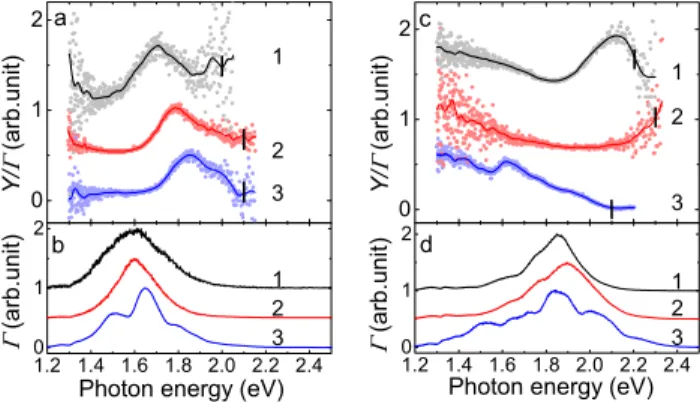
properties (Fig. 4a), except for a slight shift of the flu-orescence maximum (1.85 eV ± 0.15 eV). Similar shifts are reported in fluorescence spectra of polythiophene in solution or in thin film (from 1.6 eV to 2.2 eV) [28–30]. Conformational changes of the wires are known to im-pact the electron delocalization length and consequently the emission wavelength [31]. We speculate that this is also the case in our experimental configuration, where the suspended wires may adopt different conformations (e.g. tilting of bases) depending on the details of the lifting procedure. Experimental data provided in supplemen-tary section S8 [23] corroborate this interpretation. How-ever, distinct emission properties are observed (Fig. 4c) when the plasmon resonance maximum is centred at the same energy than the wire fluorescence (resonant con-dition). In this case, the plasmon-corrected spectrum reveals either no, strongly blue or red shifted resonances. This striking behaviour suggests that, for resonant con-ditions, more complex interaction mechanisms occur be-tween the plasmon modes and the wires states. Strong coupling between the emitter and plasmon modes [32] as well as plasmon assisted excitations of the emitter [33] are possible explanations.
Finally, it is interesting to discuss the absolute effi-ciency of the overall emission process (Q ≈ 2.5 × 10⁻⁵
photon/electron at V = 2.2 V) in the scope of the linewidth of the light emission peak (Wf ≈ 0.25 eV at
V = 2.2 V). From this last parameter we can deduce the lifetime of the excited state (τex = ~/Wf ≈ 2.6 fs) which
depends on all the possible radiative and non-radiative des-excitation channels of the molecular junction [34]. As deduced from the low emission efficiency, the lifetime of the non-radiative decay channels (τnonrad) is much
shorter than the radiative ones (τrad), and τex≈ τnonrad.
Since the emission efficiency verifies Q ≈ τnonrad/τrad, we
can estimate the lifetime for the junction emission τrad
≈ 100 ps. This value corresponds to the ratio between the intrinsic fluorescence lifetime of the wire junction and an amplification factor linked to localized plasmons [34]. Overall, τrad is approximately an order of magnitude
shorter than the radiative lifetime of polythiophene in solution [28], suggesting a plasmonic amplification of ≈ 10 [35].
Our results shed light on the electroluminescent prop-erties of single molecules bridging metallic junctions. They confirm previous theoretical works [17, 18] which predict that appropriate molecule-electrode connections may allow for intramolecular radiative transitions. We demonstrate that these transitions are directly affected by the wire conformation, the interface-induced broaden-ing of the molecular states and plasmon modes localized at the STM junction. In the scope of future applications, the polarity dependence of the emission is another re-markable property of the presented wire junctions. This strong similarity with OLEDs paves the way towards
sin-FIG. 4. (a) Plasmon–corrected light emission spectra of differ-ent wire junctions (I = 1.5 nA, 0.5 nA and 0.5 nA for spectra 1, 2 and 3 respectively) and (b) their respective plasmon am-plification functions Γ (hν) for non–resonant plasmon–emitter conditions. The Γ (hν) spectra all show a resonance around 1.6 eV, excluding an influence of the plasmons on the shifts observed in (a). The data in (c) (I = 1.5 nA, 1 nA and 1 nA for spectra 1, 2 and 3 respectively) and (d) pertain to other set of measurements where resonant plasmon–emitter condi-tions were observed. The vertical dashes mark the eV = hν quantum cut-off.
gle molecular optoelectronic components.
The authors thank Laurent Limot for stimulating discus-sions, and Jean-Georges Faullumel, Michelangelo Romeo and Olivier Cregut for technical support. The Agence National de la Recherche, contract TRANSMOL ANR-2010-JCJC-1004, the R´egion Alsace, and the Interna-tional Center for Frontier Research in Chemistry (FRC) are acknowledged for financial support.
∗ guillaume.schull@ipcms.unistra.fr
[1] M. Galperin and A. Nitzan, Phys. Chem. Chem. Phys. 14, 9421 (2012).
[2] C. W. Marquardt, S. Grunder, A. Blaszczyk, S. Dehm, F. Hennrich, H. v. Lohneysen, M. Mayor, and R. Krupke, Nat. Nanotechnol. 5, 863–867 (2010).
[3] T.-H. Lee and R. M. Dickson, J. Phys. Chem. B 107, 7387 (2003).
[4] R. Berndt, J. Kr¨oger, N. N´eel, and G. Schull, Phys. Chem. Chem. Phys. 12, 1022 (2010).
[5] X. H. Qiu, G. V. Nazin, and W. Ho, Science 299, 542 (2003).
[6] Z.-C. Dong, X.-L. Guo, A. S. Trifonov, P. S. Dorozhkin, K. Miki, K. Kimura, S. Yokoyama, and S. Mashiko, Phys. Rev. Lett. 92, 086801 (2004).
[7] E. ´Cavar, M.-C. Bl¨um, M. Pivetta, F. Patthey, M. Cher-gui, and W.-D. Schneider, Phys. Rev. Lett. 95, 196102 (2005).
[8] A. Kabakchiev, K. Kuhnke, T. Lutz, and K. Kern, ChemPhysChem 11, 3412 (2010).
[9] C. Chen, P. Chu, C. A. Bobisch, D. L. Mills, and W. Ho, Phys. Rev. Lett. 105, 217402 (2010).
Rev. Lett. 102, 057401 (2009).
[11] N. L. Schneider, G. Schull, and R. Berndt, Phys. Rev. Lett. 105, 026601 (2010).
[12] N. L. Schneider, J. T. L¨u, M. Brandbyge, and R. Berndt, Phys. Rev. Lett. 109, 186601 (2012).
[13] P. Avouris and B. N. J. Persson, J. Phys. Chem. 88, 837 (1984).
[14] G. Hoffmann, L. Libioulle, and R. Berndt, Phys. Rev. B 65, 212107 (2002).
[15] F. Rossel, M. Pivetta, and W.-D. Schneider, Surf. Sci. Rep. 65, 129 (2010).
[16] L. Lafferentz, F. Ample, H. Yu, S. Hecht, C. Joachim, and L. Grill, Science 323, 1193 (2009).
[17] J. Buker and G. Kirczenow, Phys. Rev. B 66, 245306 (2002).
[18] M. Galperin and A. Nitzan, J. Chem. Phys. 124, 234709 (2006).
[19] J. G. Keizer, J. K. Garleff, and P. M. Koenraad, Rev. Sci. Instrum. 80, 123704 (2009).
[20] G. Reecht, H. Bulou, F. Scheurer, V. Speisser, B. Carri`ere, F. Mathevet, and G. Schull, Phys. Rev. Lett. 110, 056802 (2013).
[21] M. Koch, F. Ample, C. Joachim, and L. Grill, Nat. Nan-otechnol. 11, 713 (2012).
[22] M. Magoga and C. Joachim, Phys. Rev. B 56, 4722 (1997).
[23] See supplementary material.
[24] J. Cuevas and E. Scheer, Molecular Electronics: An In-troduction to Theory and Experiment (World Scientific, Singapore, 2010).
[25] V. Mujica, M. Kemp, and M. A. Ratner, J. Chem. Phys 101, 6856 (1994).
[26] N. L. Schneider, F. Matino, G. Schull, S. Gabutti, M. Mayor, and R. Berndt, Phys. Rev. B 84, 153403 (2011). [27] Possible excitonic effects are not considered in this model. [28] G. Rumbles, I. Samuel, L. Magnani, K. Murray, A. DeMello, B. Crystall, S. Moratti, B. Stone, A. Holmes, and R. Friend, Synth. Met. 76, 47 (1996).
[29] A. Bolognesi, C. Botta, and L. Cecchinato, Synth. Met. 111-112, 187 (2000).
[30] O. J. Korovyanko, R. ¨Osterbacka, X. M. Jiang, Z. V. Vardeny, and R. A. J. Janssen, Phys. Rev. B 64, 235122 (2001).
[31] B. Xu and S. Holdcroft, Macromolecules 26, 4457 (1993). [32] A. Salomon, C. Genet, and T. Ebbesen, Angew. Chem.
Int. Ed. 48, 8748 (2009).
[33] Z. C. Dong, X. L. Zhang, H. Y. Gao, Y. Luo, C. Zhang, L. G. Chen, R. Zhang, X. T. Y. Zhang, J. L. Yang, and J. G. Hou, Nat. Photon. 4, 50 (2010).
[34] S. W. Wu, G. V. Nazin, and W. Ho, Phys. Rev. B 77, 205430 (2008).
[35] The nearly parallel orientation of the wire transition dipole moment (i.e. along the long axis of the wire) with the electromagnetic field of the excited plasmon mode (i.e. along the tip axis) leads to a much larger plasmon amplification than the orthogonal configurations [36]. This effect is balanced by the reduced amplification expected for large tip–sample distances.
[36] M. Thomas, J.-J. Greffet, R. Carminati, and J. R. Arias-Gonzalez, Appl. Phys. Lett. 85, 3863 (2004).