Chemical Vapor Deposition of Organosilicon
Composite Thin Films for Porous Low-k Dielectrics
by
April Denise Ross
M.S. in Chemical Engineering Practice Massachusetts Institute of Technology, 2001
B.S. in Chemical Engineering The University of Virginia, 1999
Submitted to the Department of Chemical Engineering in Partial Fulfillment of the Requirements for the Degree of
DOCTOR OF PHILOSOPHY IN CHEMICAL ENGINEERING AT THE
MASSACHUSETTS INSTITUTE OF TECHNOLOGY
January 2005
© 2005 Massachusetts Institute of Technology. All rights reserved.
Signature of Author... .
Signature of A uthor ...
L 1111111·.
...Department of Chemical Engineering
.~,, January 1 9, 2005
Certified
by
...
..
.
"''.
Karen K. Gleason Professor of Chemical Engineering
Thesis Supervisor
Accepted by . ... r. ... ... Daniel Blankschtein Professor of Chemical Engineering OFTECMHNOG Chairman, Committee for Graduate Students OF TECHNOL
FE 0 2 2005
!.N
1_
.AFICH .
LlI22OOJ
Chemical Vapor Deposition of Organosilicon
Composite Thin Films for Porous Low-k Dielectrics
By
April Denise Ross
Submitted to the Department of Chemical Engineering on January 1 9, 2005 in Partial Fulfillment of the
Requirements for the Degree of
Doctor of Philosophy in Chemical Engineering
ABSTRACT
Pulsed plasma enhanced chemical vapor deposition has produced organosilicon thin films with the potential use as low dielectric constant interconnect materials in
microelectronic circuits. Both diethylsilane and octamethylcyclotetrasiloxane precursors were used, with oxygen and hydrogen peroxides oxidants respectively, to deposit low-k organosilicon films. FTIR, nanoindentation, ellipsometry, and dielectric constant measurements were demonstrated as a valuable film
characterization tools to understand structure-property-processing fundamentals by quantifying structural bonding environments and relating those to the film properties. Nanocomposites were also produced using two novel techniques. First, crystal colloidal templates of polystyrene nanospheres were fabricated using evaporation-induced self-assembly. OSG was then deposited throughout the templates to create composite materials. Subsequently the polystyrene was removed upon thermal annealing to create highly porous OSG thin films. Second, ultrasonic atomization was used to deliver particles into a vacuum chamber during plasma-enhanced CVD of the organosilicon matrix to create composite thin films using an all-CVD technique. This process could extend CVD to applications currently only possible using wet processing techniques or multi-step processing.
Thesis Supervisor: Karen K. Gleason Title: Professor of Chemical Engineering
Acknowledge me nts
Though many days were spent envisioning this moment, it now surpasses my imaginable expectations, and that is due to the countless people that I owe greatly for their friendship, support, advice and guidance throughout this endeavor. To my advisor, Karen, for being an inspiring and patient mentor as well as a never-failing source of ideas and enthusiasm throughout all stages of my work. Your direction and unwavering support provided an exceptional learning environment and resulted in a thesis of which I am proud.
To my thesis committee members, Professors Paula Hammond and Herb Sawin, who generously gave their time, offered their insights, and shared their expertise.
During this time, I have had the opportunity to work alongside a truly diverse and talented group of individuals. To members of the Gleason group, past and present, I could not have asked for a more wonderful group of people from whom I have learned so much. Each of you have uniquely contributed to my work and my life. Special thanks to the members of "team low-k." Dan, for generously giving your guidance and sharing your experience, Tom, for always listening and providing conference entertainment, and Kelvin, for continually fixing my computer, always taking the time to lend a hand, and reminding me that everything will work out.
The companionship of many friends has provided my life balance over the past five and a half years. To Christy and Ley, my constant and caring friends, who have been the instigators of many good times and a source of strength during the rough times. To lan, Jim, Kevin, Kim, and Patty, my lunch crew, who provided me with daily mental health breaks filled with amusing distractions and entertaining conversations. Many additional thanks to those who enriched the quality of my life - Andrea, Anish, John, Kelvin, LaRuth, Martin, Murray, Scott, Todd, and Tom.
Most especially, to my parents, who instilled in me the importance and value of learning. Your selfless love and support never failed and is the foundation for all I have done and the inspiration for all I might achieve. No words can fully express my gratitude.
TABLE OF CONTENTS Abstract 2 Dedication 3 Acknowledgments 4 List of Figures 8 List of Tables 12 List of Notations 13 CHAPTER ONE 14 Introduction 1.1 Motivation 15 1.2 Low k Materials 18
1.3 Chemical Vapor Deposition 22
1.4 Scope of Thesis 25
References 28
CHAPTER TWO 30
Enhancement of mechanical properties of organosilicon thin films deposited from diethylsilane
Abstract 31
2.1 Introduction 32
2.2 Experimental 33
2.3 FTIR and Structure Analysis 35
2.4 Optical and Mechanical Properties 38
2.5 Effect of Processing Conditions 40
2.5.1 Flow Rate Ratios 40
2.5.2 Plasma Processing Conditions 41
2.6 Conclusions 43
48
Effects of condensation reactions on the structural, mechanical, and electrical properties of plasma-deposited organosilicon thin films from octamethylcyclotetrasiloxane
Abstract 49
3.1 Introduction 50
3.2 Experimental 52
3.3 FTIR and Structure Analysis 53
3.4 Mechanical Properties 58
3.5 Electrical Properties 63
3.6 Conclusions 64
References 66
CHAPTER FOUR 68
Nanoporous Organosilicate Glass Films via Chemical Vapor Deposition onto Colloidal Crystal Templates
Abstract 69
4.1 Introduction 70
4.2 Experimental 72
4.2.1 Formation of Templates 72
4.2.2 Pulsed-Plasma Enhanced Chemical Vapor Deposition 73
4.2.3 Characterization Methods 74
4.3 Optical and Mechanical Properties 75
4.4 Conclusions 83
References 84
CHAPTER FIVE 86
Chemical Vapor Deposited nanocomposites Fabricated Via Ultrasonic Atomization
Abstract 87
5.1 Introduction 88
5.2 Experimental 90
5.3 Results and Discussion 93
5.4 Conclusions 103
References 106
CHAPTER SIX
Conclusions & Future Directions
6.1 Conclusions
6.1.1 OSG Matrix Materials 6.1.2 Composite Materials 6.2 Future Directions APPENDIX A Reactor Configurations 108 109 109 110 112 113
-List of Figures
CHAPTER ONE
Figure 1-1: Schematic representation of relevant physical dimensions for the RC delay.
Figure 1-2: Dielectric constant for varying degrees of porosity. Figure 1-3: Characteristic diffusion times for small molecules. Figure 1 -4: Schematic of typical PECVD vacuum reactor.
CHAPTER TWO
Figure 2-1: FTIR Spectra of a film as-deposited (solid line) and annealed (dashed line).
Figure 2-2: FTIR Spectra of a film as-deposited and annealed, highlighting the silanol bonding region.
Figure 2-3: Displacement into surface versus hardness plot for as-deposited (open markers) and annealed (solid markers) films, with significant increase seen upon annealing.
Figure 2-4: Displacement into surface versus elastic modulus plot for as-deposited and annealed films, with significant increase seen upon annealing.
Figure 2-6: Effect of precursor flow rate ratios on hardness.
Figure 2-7: Effect of precursor flow rate ratios on elastic modulus.
Figure 2-8: Refractive indices and deposition rates versus plasma pulsing conditions.
CHAPTER THREE Figure 3-1: Figure 3-2: Figure 3-3: Figure 3-4: Figure 3-5: Figure 3-6: Figure 3-7: Figure 3-8:
FTIR Spectra of films as-deposited at varying oxidant flow rates. (b) expansion of hydroxyl bonding region (c) expansion of Si-(CH3)x
bonding region.
Effect of oxidant flow rate on ratio of T groups to D groups, determined by spectral curve fitting.
FTIR Spectra of a film as-deposited (solid line) and annealed (dashed line). (b) expansion of hydroxyl bonding region (c) expansion of Si-(CH3)x bonding region.
Displacement into surface versus hardness plot for as-deposited (open markers) and annealed (solid markers) films, with significant increase seen upon annealing.
Displacement into surface versus elastic modulus plot for as-deposited and annealed films, with increase seen upon annealing. Effect of oxidant flow rate on hardness and elastic modulus. Hardness versus connectivity number.
Effect of oxidant flow rate and annealing on the dielectric constant.
CHAPTER FOUR
Figure 4-1: Figure 4-2:
Figure 4-3:
Figure 4-4:
Schematic of self-assembly of a colloidal crystal template.
SEM images of a five-layer polystyrene template assembled on Si wafer from 96 nm polystyrene nanospheres : (a) Top view; (b) Oblique view.
FTIR spectra of (a) the template polystyrene nanospheres; (b) the composite film consisting of the template of polystyrene nanospheres filled with CVD OSG and (c) porous OSG film resulting from the
decomposition of the polymer beads upon annealing.
AFM of composite materials with OSG deposition rates of (a) 45.8 nm/min and (b)72.0 nm/min.
Figure 4-5: Images of porous structures (a) SEM images of nanoporous OSG using 96nm bead template (b) TEM image of nanoporous OSG film using the 15nm bead template.
Figure 4-6: Plots of (a) the refractive index versus template percentage and (b) the dielectric constant versus template percentage.
CHAPTER FIVE Figure 5-1: Figure 5-2: Figure 5-3: Figure 5-4: Figure 5-5: Figure 5-6:
Reactor configuration of simultaneous plasma-enhanced deposition of matrix material and ultrasonic atomization deposition of particles. Fluorescent microscopy of composite thin films consisting of OSG matrix and fluorescently labeled dextran particles.
FTIR spectra of (a) pure fluorescently labeled dextran (b) pure OSG matrix material and (c) the composite material.
Fluorescent microscopy of composite OSG films with labeled dextran where the later was delivered by ultrasonic atomization from aqueous solutions of varying ethylene glycol content (a) 100% (b) 95% (c) 90% and (d) 80% ethylene glycol. The volatility of the solvent greatly effects the particle deposition. The pure ethylene glycol has a comparatively low volatility, and does not evaporate before striking the substrate. Water, with a much higher volatility, evaporates quickly leaving only
the dextran crystals to descend onto the substrate.
Calculated effect of reactor pressure on the droplet lifetime of ethylene glycol.
Fluorescent microscopy of OSG films with labeled dextran where the ultrasonic atomization of the dextran employed 100% ethylene glycol at (a) 150mTorr and (b) 500 mTorr. The evaporation driving force is fueled by the difference in the solvent saturation pressure and reactor pressure, and as the reactor pressure increases to 500 mTorr and approaches the saturation pressure, no solvent evaporation occurs and the droplets strike the substrate with their original diameter of 45 gm.
Figure 5-7:
Figure 5-8:
FTIR spectra of annealed composite thin film and (inset) fluorescent microscopy of annealed films. Both indicate removal of dextran particles.
SEM image of porous OSG matrix structure with 96nm pores, originally a composite film with polystyrene microbeads.
APPENDIX A Figure A-1: Figure A-2: Figure A-3: Figure A-4: Figure A-5:
Basic reactor configuration accommodating an ultrasonic atomizer. Basic reactor configuration accommodating an ultrasonic atomizer, overhead view.
CAD drawing of redesigned reactor lid accommodating ultrasonic atomizer (top view).
CAD drawing of redesigned reactor lid accommodating ultrasonic atomizer (side view).
Detailed drawing of redesigned showerhead accommodating ultrasonic atomizer.
List of Tables
CHAPTER ONE Table 1-1: Table 1-2: Table 1-3: Levels of metallizationSIA Roadmap indicating demand for low-k technology Polarizability of common bonds
CHAPTER THREE
Table 3-1: Structural numbers
composition percentages from FTIR and connectivity
CHAPTER FIVE
List of Acronyms, Abbreviations, and Symbols
Absorbance Capacitance
Chemical Mechanical Polishing Continuous Random Network Chemical Vapor Deposition Continuous Wave
Film Thickness Diethylsilane Droplet Diameter
Diffusion Coefficient of Solvent Octamethylcyclotetrasiloxane Elastic Modulus
Ethylene Glycol Vacuum Permittivity
Environment, Safety and Health Frequency
Fourier Transform Infrared Spectroscopy Gigapascals
Hardness
Mass Rate of Evaporation
International Technology Roadmap for Semiconductors Interferometry for Thermal Stability
Dielectric Constant Index of Refraction Mean Squared Error Molecular Weight Power
Plasma-Enhanced Chemical Vapor Deposition Partial Pressure at the Droplet's Surface Pulsed Laser Deposition
Pulsed Plasma-Enhanced Chemical Vapor Deposition Partial Pressure of Solvent in the Reactor
Resistance Gas Constant Radio Frequency
Average Connectivity Number Density of the Drop Liquid
Standard Cubic Centimeters per Minute Organosiloxane / Carbon Doped Oxide Droplet Lifetime
Temperature Tetraethoxysi lane
Variable Angle Spectroscopic Ellipsometry A C CMP CRN CVD CW d DES dp Dv D4 E EG so ESH
f
FTIR GPa H I ITRS ITS k n MSE M, MW P PECVD Pd PLD PPECVD P R R RF <r> PP sccm SiCOH t T TEOS VASECHAPTER ONE
1.1 MOTIVATION
The demand for high-speed devices in today's electronics is surging and several changes are being investigated for improvement of current devices. At the forefront of these options is reducing the resistance, R, of the wire interconnects and reducing the capacitance, C, between the wires.' Reducing the wire resistance
is especially important as chip and wire size decreases, since the resistance is inversely proportional to the cross sectional area of the wire.' Since 1965, Moore's Law, which states that the number of transistors on a computer chip doubles roughly every eighteen months, has compelled the drive for miniaturization.2 One option recently implemented involved substituting copper for the standard aluminum metallization with tungsten plugs. Copper offers both a lower resistivity, 1.7 !gQ-cm compared to 3.0 pQ-cm, and improved electro-migration resistance.' Transistor speed can be quantified by the RC delay, which is the intrinsic time delay
for signal propagation, and is given in the equation below
_RC _, L___ kepL2M
=
=(
1JkEWmTm
)
=
TdTm
1-1
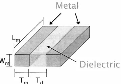
Figure 1-1 depicts the relative physical dimensions referred to in equation 1-1. Holding all dimensions constant, only the metal resistivity, p, and the dielectric constant, k, can be manipulated. By lowering the resistivity of the metal the RC delay time, , is decreased proportionally.
Metal
./'
Dielectric
Figure 1-1: Schematic representation of relevant physical dimensions for the RC delay.
Reducing the dielectric constant, and thereby the capacitance, of the interlevel material is another viable option for reduction of the RC delay. In addition, this change can also reduce power consumption, P, which is particularly important in small, portable devices, and cross talk noise, N, between adjacent metal lines.
N _Cline-lo-line Clolal
1-2
1-3
Therefore, by choosing to decrease the dielectric constant, the designer is afforded a higher degree of freedom.3 Another driving force for lower metal resistivity and dielectric capacitance is that fewer levels of metallization are required for a fixed degree of functionality, as shown in Table 1-1 . Fewer metal
layers lead to less materials, less energy, and less waste as well as decreased device
complexity.'
Table 1-1: Levels of metallization
CD
k=4 k=2 k=4 k=2
(pLm) Al Al Cu Cu
0.18 8 6 6 4
0.1 14 11 11 7
Once realized, the integration of theses new low-k materials into current device construction has proved to be an additional challenge for manufacturers. The ITRS Roadmap, which outlines where the technological requirements for the
semiconductor industry, illustrates these difficulties, as the expectations for dielectric constant reduction has been notably delayed between 2001 and 2003, as shown below in Table 1-2.3 In year 2007 at the 65nm technology node, the 2001 projection indicated an effective dielectric constant of 2.3 to 2.7 would be mandated. In the two years before the 2003 roadmap publication, significant difficulties had been encountered to cause that value to increase to 2.7 to 3.0. At the time of publication, solutions for these values were still unknown.
Table 1-2 Year Technology Node 2001 ITRS Roadmap 2003 ITRS Roadmap
: SIA Roadmap indicating demand for 2001 2003 2004 2007 130 130 90 65 3.0-3.6 3.0-3.6 2.6-3.1 2.3-2.7 3.3-3.6 3.1-3.6 2.7-3.0 low-k technology 2010 2013 45 32 2.1 1.9 2.3-2.6 2.0-2.4 2017 22 1.8 2.0 =
1.2 LOW-K MATERIALS
Two different pathways can be explored, independently or together, to lower the k-value relative to SiO2 (k-4), once the industry standard. Both incorporating
atoms and bonds that have a lower polarizability and decreasing the density of the material reduce the dielectric constant. Both of these avenues can be related to the overall polarization, P, of the material. All matter is made of electrically charged
particles, electrons and nuclei combining to form atoms, molecules, and ions.4 When brought into an external electric field (E), the forces acting upon the charges
bring about a small displacement of the electrons relative to the nuclei. Polarization is the acquired dipole moment per unit volume in response to an applied electric field. The dielectric constant can be related to the polarizability by the following equation.
k =l+
E 1-4
The dielectric constant is dependent on temperature, density or pressure, and chemical composition. Polarization includes three parts arising from the electronic, atomic and orientation responses of the material, each corresponding with the motions of a different kind of microscopic particles with different characteristic times.4'5 At high frequencies, the electronic response dominates and the dielectric constant equals the square of the optical index of refraction, k = 2.
Table 1-3 shows some typical polarizabilities of common bonds.5 This indicates that single bonds, particularly C-C, C-F, and C-O, have the lowest polarizabilities, as double bonds have increased mobility of the 7C electrons.
oxides, or organosilicate glasses (OSGs) and fluorinated hydrocarbons. OSG have two main advantages. The Si-C bonds are more covalent in nature than the Si-O
bonds, since Si and O have a large electronegativity difference giving ionic character to their bond and increasing polarizability. Also by adding methyl (-CH3) groups bound to Si atoms, a proportion of the Si-O bonds are terminated resulting in a "loosening" of the lattice as lighter C and H atoms replace the densely packed Si and O crosslinked network; therefore, a reduction in the film density and dielectric constant is achieved.5'6
Table 1-3: Polarizability of common bonds Bond Polarizability (A3 ) C-C 0.531 C-F 0.555 C-O 0.584 C-H 0.652 O-H 0.706 C=O 1.02 C=C 1.643
Current dense OSG films have dielectric constants ranging from 2.7 to 3.3.7
-'9 Another method of loosening the lattice involves the addition of fluorine into the film. Fluorine atoms exhibit particularly high electronegativity, which facilitates tight binding of electrons and decreased polarizability.5 However, fluorine addition can also degrade the stability of the film.3'20
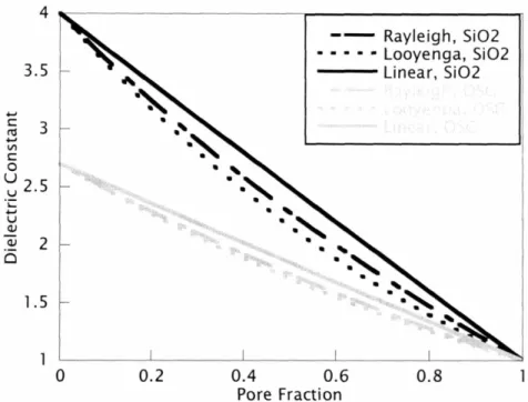
The introduction of void space, which has a k-value of 1.0, the theoretical lower limit for k, is another approach for the reduction of dielectric constants in thin films. Voids can be introduced into the materials through air bridge fabrication or by creating nano-porous films. Many of these film's properties depend on the degree of porosity, p, where the air bridge would have the highest porosity of 1. There are many models that predict the effective dielectric constant
for heterogeneous mixtures.4 The Rayleigh model assumes the pores are a uniform distribution of spheres in a cubic lattice, while the Looyenga model assumes spheres of mixed composition. Figure 1-2 depicts how the dielectric constant changes with degree of porosity for these models for both silicon dioxide and a typical OSG with fully dense dielectric constant of 2.7.
4 3.5 ... ~ 3 ... III C o U u 2.5 .~ ... u Q) Q) 2 o 1.5 -- Rayleigh, Si02 •••• • Looyenga, Si02 Linear, Si02 0.8 0.2
o
0.4 0.6 Pore FractionFigure 1-2: Dielectric constant for varying degrees of porosity.
It is clear from this graph that porosity plays a secondary role to matrix material in lowering the dielectric constant. While ample research continues to investigate reducing the dielectric constant of dense OSG materials further, their extension to ultra-low dielectric constant application is limited by material properties. In order to meet all of ITRS requirements outlined in Table 1-2, porosity will eventually be necessitated. Although increased porosity is favorable for the dielectric constant, the film has other characteristics that suffer as porosity is increased. Mechanical strength is reduced with porosity, p, by (l_p)3 while thermal cond uctivity is reduced by (1 _p)1.5.5
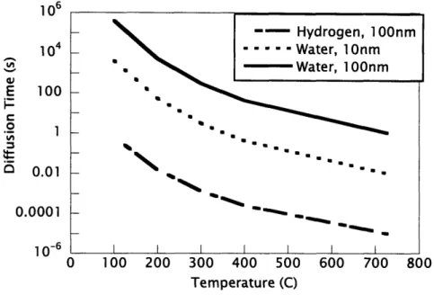
With current feature size in the 100 nm range, it is imperative that the pore size remains below 1 Onm and have a small distribution. Any pores larger than 10 nm could be considered defects and can affect mechanical strength. Currently under debate is whether the pores should be open or closed on a microstructural level. Open pores are connected throughout the film and occur at porosities greater than approximately 30%. Some believe the closed pore structure is better as it would help relieve low-k voiding, which occurs when fluorinated etch gas used in later processing step permeates into the voids. If then annealed, the pores can coalescence, forming macroscopic voids.21'2 2 The idea behind closed pore
structures is that it would prevent the diffusion of the etch gas into the pores. However, when dealing with small molecules such as fluorine at typical processing temperatures (4000C) the characteristic diffusion times through silicon dioxide are short, indicating that the etch gas would diffuse into the pores whether open or closed. Figure 1-3 shows the characteristic diffusion times through varying depths of silicon dioxide for other small molecules as a function of temperature. Additionally, an OSG matrix would be significantly less dense allowing even faster diffusion of molecules through the film.
I 04 E 100 i= 0.000 0 11 F-6 -- Hydrogen, l00nm _ . . .Water, 10 nm _ ' . Water, 100nm -", I I I I I I I 0 100 200 300 400 500 600 700 800 Temperature (C)
Figure 1-3: Characteristic Diffusion Times for small molecules
Throughout these processing steps, it is important that the film maintain certain properties essential for any low-k film; these properties include thickness, uniformity, refractive index, adhesion, chemical resistance, thermal stability, pore size and distribution, coefficient of thermal expansion, glass transition temperature, film stress, and value of the diffusion coefficient for copper.2 3
1 .3 CHEMICAL VAPOR DEPOSITION
Several different methods are routinely used for depositing low-k materials. The main dichotomy is between spin-on dielectric (SOD) and chemical vapor deposition (CVD), each with its advantages and disadvantages. Manufacturers of spin-on materials claim better extendibility to future generations because of the demonstrated ability to add pores, especially in the sub-2.5 range when porous low-k material will be required. These materials begin as a dense blend of two substances, one of which is later decomposed to create the porous structure. This type of hybrid system is referred to as a matrix-porogen composite. Thus far, SOD
has demonstrated higher capabilities to produce porous low-k materials using this technique.4 23-26 Yang et. al. has produced porous thin films using cyclic silsesquioxane as the matrix material and thermally labile cyclodextrin molecules as the porogen, with resulting dielectric constants as low as 1.9. However, SOD has several drawbacks, primarily from an environmental, health, and safely viewpoint. It requires the use of a solvent to distribute the polymers and often a subsequent rinsing step, both of which have significant waste and can expose workers to chemicals and out-gassing. Additionally, wet processes are often limited by the solubility of polymers and problems can occur when fabricating composite materials with the aggregation of particles.
On the other hand, CVD manufacturers claim more reuse of existing toolsets and simpler integration due to silicon dioxide-like structure of CVD siloxanes.2 3 CVD processes excel at producing thin, conformal coatings with low levels of contaminants when high purity precursors are used. Chemical vapor deposition is a more environmentally friendly manufacturing method that utilizes gas phase chemistries in a low to ultra-low pressure environment to produce well-defined, high quality films in a controllable and tunable fashion.2 7 CVD involves several steps: creation of reactive species in the gas phase, transport to the substrate surface, adsorption of onto the surface, diffusion on the surface, polymerization and film growth, and desorption of volatile, non-polymerized species.2 8 Furthermore, vacuum techniques such as CVD have limited worker chemical exposure and no waste solution.
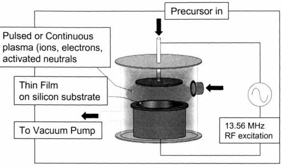
Plasma-enhanced CVD (PECVD) occurs when a low-density plasma is generated by radio frequency excitation of the precursor gas. The plasmas are composed of ions, radicals, and excited neutrals from the gas that react on a temperature-controlled substrate to form a film.27 A typical PECVD reactor is depicted in Figure 1-4.
Pulsed or Continuous plasma (ions, electrons, activated neutrals Thin Film on silicon substrate
"'1'
To Vacuum PumpI
Precursor in...
13.56 MHz RF excitationFigure 1-4: Schematic of typical PECVDvacuum reactor
Continuous wave plasmas are commonly used and occur when a constant
electric field is applied for the entire duration of the deposition. At higher powers,
the precursor molecules undergo more fragmentation which produces highly
crosslinked films bearing little resemblance to the original precursor structure.
Additionally, at high powers, polymerization often begins in the gaseous phase,
leading to unwanted particle generation.29 The polymers also tend to show aging
effects upon exposure to the atmosphere as well as a higher number of free
radicals or dangling bond due to ion bombardment.
Alternatively, pulsed plasma-enhanced CVD (PPECVD)occurs when the
electric field is turned on and off in a distinct pattern, with times in the millisecond
range. The equivalent power is calculated by multiplying the duty cycle, which is
the percent of time the plasma is on, by the peak power of the plasma. For
example, a 10 ms - 40 ms on-ff pulse cycle with a 300 watt peak power would be
effects and reducing the number of dangling bonds, PPECVD also provides another parameter with which to further fine tune the properties of the thin films.
The semiconductor industry has struggled with determining an all CVD approach to creating porous, low-k materials. Most research in this area focuses on simultaneously co-depositing the matrix, normally silicon dioxide based, and the porogen, usually an organic species, from two or more precursors.30-32 Problems occur from the compatibility of the deposition conditions needed to produce two very different polymers simultaneously.
1.4 SCOPE OF THESIS
This thesis investigates OSG thin films deposited by PPECVD, studying the structure-property-processing relationship, and establishes an all-CVD approach to creating matrix-porgen composites using a novel manufacturing technique. It is structured into four main technical chapters, each a published journal article and as such can be read as self contained works.
CHAPTER TWO reports on the plasma polymerization of OSG thin films deposited from diethylsilane and oxygen precursors. The additional organic content of diethylsilane compared to traditional methyl-doped precursors was selected to increase the carbon content in the film, which is known to improve electrical properties. Changes in mechanical properties observed with annealing were placed in context of reactions occurring between proximal end groups.
CHAPTER THREE presents results from organosilicon thin films deposited from octamethylcyclotetrasiloxane and hydrogen peroxide using pulsed-plasma enhanced chemical vapor deposition. Hydrogen peroxide was used as an oxidant to promote hydroxyl incorporation into the film structure. Annealing generated condensation reaction throughout the film, altering its composition and properties.
FTIR analysis was used to link the film structure with its electrical and mechanical properties and the work was placed within the framework of the percolation of rigidity.
CHAPTER FOUR establishes a two-step technique for the fabrication of porous OSG materials. Evaporation-induced self-assembly was used to create templated polystyrene microbead arrays of well-defined and controllable thicknesses. PPECVD was used to deposit a matrix OSG from silane precursors in and throughout the bead template. Subsequent annealing decomposes the polystyrene to form a porous OSG thin film.
However, this process is unable vary the degree of porosity and is comprised of multiple steps, including a wet process. The process was modified slightly using
a layering technique, whereby layers of polystyrene beads are alternated with OSG deposition. While this adjustment offers improved control over percent porosity, it adds extra steps and increases the complexity of the process.
CHAPTER FIVE introduces a novel technique implement to create composite thin films with an all-CVD process. Films were fabricated by employing ultrasonic atomization to introduce the porogen particles into the vacuum chamber during plasma-enhanced deposition of a matrix material. Fluorescently labeled dextran particles were employed to allow direct observation of the dextran within the matrix film. Particle deposition was explored in the context of solvent properties as well as reactor conditions. This process could extend the CVD technique to applications for composite materials currently only feasible using wet processing techniques or multi-step processing.
CHAPTER SIX presents some concluding thoughts about the work and comments on possible further directions that this research might take, based on the results presented.
This work would not have been possible without the generous support of the NSF/SRC Engineering Research Center of Environmentally Benign Semiconductor Manufacturingand the SRC / Texas Instruments for their support through the Graduate Fellowship Program.
REFERENCES
1. M. T. Bohr, Solid State TechnoL 39, 105 (1996). 2. G. E. Moore, Electronics 38, 1 (1968).
3. M. B. Anand, M. Yamada, and H. Shibata, IEEE Trans. Electron Devices 44, 1965 (1997).
4. C.J. F. Bottcher, O. C. van Belle, P. Bordewijk, and A. Rip, Theory of Electric
Polarization, 2nd ed (Elsevier Scientific Pub. Co., New York, 1 973).
5. M. Morgen, E. T. Ryan, C. H. Jie-Jua Hua, T. Cho, and P. S. Ho, Annu. Rev. of Mater.
Sci. 30, 645 (2000).
6. D. Thomas, Y. Song, and K. Powell, Solid State Technol. 44, 107 (2001). 7. D. D. Burkey and K. K. Gleason, J. Appi. Phys. 93, 5143 (2003).
8. D. D. Burkey and K. K. Gleason, J. Electrochem. Soc. 1 51, F1 05 (2004). 9. A. Grill, Thin Solid Films 398, 527 (2001).
10. A. Grill, V. Patel, and C. Jahnes, 145, 1649 (1998). 11. A. Grill and V. Patel,J. AppI. Phys. 85, 3314 (1999).
12. A. Grill and D. A. Neumayer, J. Appl. Phys. 94, 6697 (2003).
13. C.-T. Lin, F. Li, and T. D. Mantei, J. Vac. Sci. Technol. A 17, 735 (1999).
14. L. Peters, Semiconductor International (May 2002). 15. Q. G. Wu and K. K. Gleason, Plasmas Polym. 8, 31 (2003).
16. Q. G. Wu and K. K. Gleason,J. Vac. Sci. Technol. A 21, 388 (2003).
17. J. Widodo, W. Lu, S. G. Mhaisalkar, L. C. Hsia, P. Y. Tan, L. Shen, and K. Y. Zeng, Thin
Solid Films 462-63, 213 (2004).
18. E. S. Lopata, L. Young, andJ. T. Felts, Mater. Res. Soc. Symp. Proc. 612, D5.3.1
(2000).
19. M. J. Loboda, Microelectron. Eng. 50, 1 5 (2000).
20. L. Peters, Semiconductor International (September 1 998).
21. R. P. Mandal, D. Cheung, P. W.-M. Lee, and C.-l. Lang, USA Patent No. 207791 (August 22 2000).
22. R. P. Mandal, D. Cheung, and W.-F. Yas, USA Patent No. 1 77044 (January 9, 2001 2001).
23. L. Peters, Semiconductor International (June 2000).
24. A. T. Kohl, R. Mimna, R. Shick, L. Rhodes, Z. L. Wang, and P. A. Kohl, Electrochem.
25. R. D. Miller, Science 286, 421 (1999).
26. M. Gallagher, T. Adams, C. Allen, N. Annan, R. Blankenship, J. Calvert, W. Fillmore, R. Gore, D. Gronbeck, S. Ibbitson, C. Jehoul, A. Lamola, G. Prokopowicz, N. Pugliano, C. Sullivan, M. Talley, and Y. You, Abstr. Pap. Am. Chem. Soc. 224, U510 (2002).
27. R. D'Agostino, Plasma deposition, treatment, and etching of polymers (Academic Press, Boston, 1 990).
28. M. L. Hitchman and K. F. Jensen, Chemical Vapor Deposition, Principles and
Applications (Academic Press, New York, 1 993).
29. H. Yasuda, Plasma Polymerization (Academic Press, Inc., Orlando, 1985). 30. A. Grill and V. Patel, Appl. Phys. Lett. 79, 803 (2001).
31. A. Grill, J. Appl. Phys. 93, 1785 (2003).
CHAPTER TWO
ENHANCEMENT OF MECHANICAL PROPERTIES OF ORGANOSILICON THIN FILMS DEPOSITED FROM
DIETHYLSILANE
ABSTRACT
Pulsed-plasma enhanced chemical vapor deposition was used to deposit organosilicon thin films from diethylsilane and oxygen. FTIR analysis shows significant organic content as well as hydroxyl and silanol moieties present in the as-deposited materials. FTIR showed a complete removal of hydroxyl groups after annealing at 400 C for 1 hour. This indicates a condensation reaction between proximal hydroxyl groups leading to the formation of additional Si-O-Si linkages, which would increase the mechanical properties of the film. Mechanical property measurements were in accordance with this hypothesis, as both the hardness and modulus increased by over 50% after annealing. Film structure and properties were strongly dependent on the precursor feed ratio.
2.1 INTRODUCTION
The demand for high-performance electronic devices is surging, motivating research into improvements of interconnect speed. One of these options is reducing the capacitance, C, between the wires via the dielectric constant. This is not only a option for reduction of the RC delay, but can also reduce power consumption, P, and cross talk noise, N, between adjacent metal lines.' One important class of low-k materials is the carbon-doped silicon oxides, also known as organosilicate glasses (OSGs).2'3 OSGs have two main advantages. First, the Si-C bonds are more covalent in nature than the Si-O bonds, since Si and O have a large electronegativity difference giving ionic character to their bonds leading to increased polarizability and hence higher dielectric constants.4 Additionally, by adding organic content such as methyl (-CH3) and ethyl (-CH2CH3) groups bound to Si atoms, a proportion of the Si-O bonds are terminated resulting in a "loosening" of the lattice as lighter C and H atoms replace the densely packed Si and O
crosslinked network; therefore, a reduction in the film density and k-value is achieved.3 4 Current research of dense OSG films has generated dielectric constants ranging from 2.4 to 3.3.5-8 Improvement of mechanical properties is essential for successful integration of OSG films in advance microelectronic devices.9
The CVD OSG films have found wide acceptance in semiconductor manufacture.'0 CVD utilizes gas phase chemistries in a low to ultra-low pressure environment to produce well-defined, high quality films in a controllable and tunable fashion." This work focuses on OSG thin films created from diethylsilane (DES) and oxygen. The DES precursor has previously been used to produce both SiO2 and SiNCH thin films using a variety of methods for number of different application targets.'2 -20 Silane precursors such as methylsilane, dimethylsilane and trimethylsilane have often been utilized to create OSG dielectric materials, and
dielectric constants for trimethylsilane (3MS) and 02 have been shown in the range
of 2.4 to 3.0 using PECVD.7 2'1 However, these silanes are generally highly explosive and therefore present considerable health and safety hazards. DES is more environmentally benign precursor and is an evolutionary step toward achieving higher organic content through the addition of ethyl groups instead of methyl groups in OSG materials.
The addition of organics to the dielectric results in a more open structure, reducing density and network bonding, both of which contribute to reduced mechanical properties. This creates issues with latter processing steps, such as the ability to survive chemical-mechanical polishing.2 '9 Spin-on deposition, another
technique sometimes used for low-k materials, relies on a thermal curing step that leads to a structural transformation which supplies the material's strength.2 2 2 6 Often utilizing alcohol or water condensation chemistry, reactions between
proximal end groups help to crosslink the film, thereby making it mechanically robust. In this work, the ability of condensation chemistry to improve the mechanical properties of CVD OSG films is explored.
2.2 EXPERIMENTAL
Depositions were carried out in a custom-built, parallel-plate vacuum chamber. The PECVD system has an upper electrode powered by a 13.56 MHz RF source (ENI HF650) with attached matching network (Heathkit SA2060-A) and a grounded lower electrode. The lower electrode also functions as the substrate stage and was kept at room temperature using a water cooled system. In addition, electrostatic clamping capabilities were utilized to help maintain constant substrate temperatures. The substrates used were 100 mm diameter silicon wafers. The upper electrode / shower-head distributes all incoming precursor gases over the
substrate. Diethylsilane (DES, Gelest Inc., CAS 542-91-6, > 95%) was the monomer used with no further purification. The DES was volatilized in a glass jar and delivered to the reactor chamber through a calibrated needle valve. Oxygen and argon were delivered to the reactor using a UNIT Instrument URS-100 Mass Flow controlling system. For all depositions, chamber pressure was maintained at approximately 300 mTorr and is controlled by a butterfly valve (MKS 253B) connected to an MKS model 651C exhaust valve controller. When investigating thermal stability, films were annealed at 400 C and ambient pressure in a nitrogen atmosphere for one hour.
Fourier Transform Infrared (FTIR) Spectroscopy was performed on a Thermo Nicolet Nexus 870 ESP spectrometer in transmission mode at 4 cm-' resolution using 64 scan averaging. A 10 minute nitrogen purge was performed between each measurement to diminish the effects of carbon dioxide and moisture. All spectra were baseline corrected and had their intensity normalized to a thickness of 5000 A
using their measured thicknesses and Beer's Law.
Film thicknesses and indices of refraction (n633) were determined using VASE, Variable angle spectroscopic ellipsometry, performed on A Woolam M-2000 spectrometer having a xenon light source.. Data was acquired at three angles (650, 700, and 75°). The Cauchy model2 7 was used to fit the data and the mean-squared errors (MSE) was low (<10), signifying a match between the model and the data. In addition to quantifying the optical properties, the refractive index also gives an indication of the electrical properties, as the square of the refractive index is the lower limit of the dielectric constant. This approximation is most appropriate in insulating materials having the smallest induced dipoles and takes into consideration only electronic polarization.28'2 9 This measure will be used to gauge the electrical properties because dielectric constant measurements using a mercury probe can be error prone due to their high sensitivity to films thickness.
Mechanical properties were measured at the Novellus Research Center in Tualatin, Oregon. Measurements of hardness and elastic modulus were performed using a MTS Systems Nano-lndenter XP and MTS patented continuous stiffness measurement technique. With this technique, each indent gives hardness and elastic modulus as a continuous function of the indenter's displacement into the samples. The surface approach velocity was 5nm/s and the load versus displacement slop was -81.6 N/m. Experiments were terminated at a depth of approximately 300 nm. A Berkovick diamond tip was used in the measurements. The films were 1 m or greater in thickness to minimize any substrate effects on
the results. Fused silica was tested and used as a control sample.
2.3 FTIR AND STRUCTURE ANALYSIS
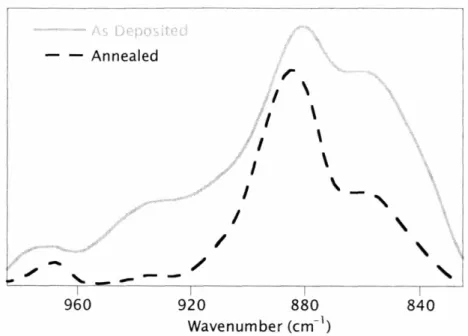
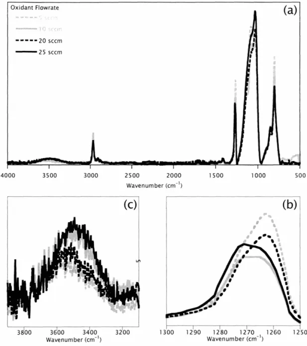
Figure 2-1 shows the FTIR spectra of film deposited from a mixture of DES and 02, both as-deposited and after annealing. The deposition was carried out with flow rates of 7 sccm of DES, 20 sccm of 02, and 6 sccm of argon using 10/70 ms on-time/ms off-time pulsed plasma excitation and 300W peak power. The assignments of the FTIR bands for OSG materials have been previously reported.3 0 The peaks in the 3000 - 2850 cm-' region correspond -CH3and -CH2, revealing the significant presence of hydrocarbon content in the film. The definite presence of the -CH2peaks at 2920 and 2950 cm-' indicates either the existence of intact ethyl groups or methylene bridging. The broad peak at 3700-3200 cm-' shows considerable free -OH inclusion in the as-deposited film, most likely due to incorporation of impurities such as water and silanol moieties. Hydroxyl incorporation also appears around 920-830 cm-', signifying the stretch of the silanol (Si-OH) bond, as shown in Figure 2-2. Also located in this region of the spectrum is Si-C bond, which extends from 870 to 750 cm-' for the Si-CH3 rock
and from 975-945 cm-l for Si-CH2CH3. The peaks between 2280 and 2080 cm-l show the presence of Si-H in the films. The Si-Q-Si backbone absorbance appears between 1000 and 1200 cm-l, with the rightmost adsorption peak centered around
1060 cm-l. This characteristic peak is associated with longer chain siloxanes. The
broad shoulder to the left of this peak is indicative of a more complicated network structure. Si-(CH3)x symmetric stretching bands occur between 1240-1 300 cm-l .
However, this area is largely overshadowed by the broadened Si-Q shoulder which encompasses Si-CH2CH3 at 1250-1220 cm-l as well as Si-CH2CH2-Si at 1180-1120
ftC:Cj - - Annealed /"-', .,..~~.-#/, ~.,. 4000 3500 3000 2500 2000 Wavenumber (em-I)
Figure 2-1 : FTIR Spectra of a film as-deposited (solid line) and annealed (dashed line).
- - Annealed
-960 920 880 840
Wavenumber (em-I)
Figure 2-2: FTIR Spectra of a film as-deposited and annealed, highlighting the silanol bonding region.
After annealing, significant changes can be observed in the film structure.
Most notably, the broad -OH peak at 3700-3200 cm-1
disappears, indicating
complete removal of the hydroxyl group after annealing. Correspondingly, the
peaks assigned to the silanol bond at 830 - 920 cm-1 show a significant decrease,
particularly in the peak at 850 cm-1, further implicating the removal of the silanol
moieties. However, these peaks do not vanish completely as this region is filled
with various other stretches. Another apparent difference is the increase in
intensity of the Si-O-Si peak at 1060 cm-1
, indicating the formation of additional
Si-O linkages. Combined, these two variances can be attributed to adjacent Si-OH
groups undergoing a condensation reaction as outlined below.31-33
",Si-OH + HO-Si", ~ ....Si-O-Si .... + H20t
This reaction facilitates the creation of additional Si-O networking resulting
in a higher crosslinked film and improved mechanical strength.30 In the absence of
2.4
OPTICAL AND MECHANICAL PROPERTIESBoth the optical and mechanical film properties were examined before and after annealing. Film thickness retention after annealing was >90% demonstrating reasonable thermal stability. The refractive index decreased from 1.442 to 1.430 after annealing, partially due to the loss of -OH from the film. Additionally, the reduction in film density brought about by the loss of water in the condensation reaction and increased crosslink formation would also contribute to a lower index of refraction.
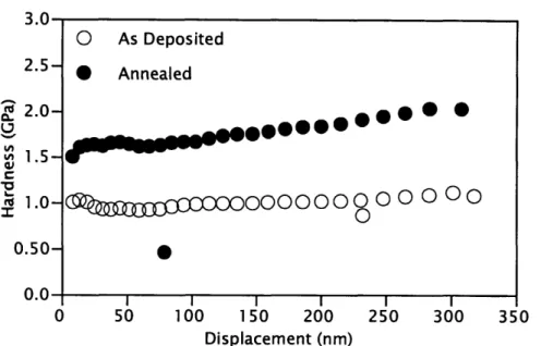
Figure 2-3 shows the hardness versus displacement curves for the as-deposited and annealed films; Figure 2-4 shows modulus versus displacement.. For both hardness and modulus, a substantial increase is seen upon annealing. Hardness increased over 70% from 0.98 to 1.67 GPa, while the modulus jumped from 6.84 to 10.58 GPa, a 54% increase. This change is consistent with the condensation reaction creating a more crosslinked film, as confirmed by the FTIR analysis. These results strongly suggest that higher crosslinking leads to a more rigid, mechanically stable structure. Changes in mechanical properties as a result of crosslinking in OSG films induced during anneal have previously been reported, with hardness increasing between 1-20% and the modulus declining,3 0 the changes reported here are much more dramatic.
3.0 2.5-I 2.0-v O 1.5-to 1.0- 0.50-n I I I I I I 0 50 100 150 200 250 300 350 Displacement (nm)
Figure 2-3: Displacement into surface versus hardness plot for as-deposited (open markers) and annealed (solid markers) films, with significant increase seen upon annealing.
30 25 20 Ll . 15 10 5 0 Displacement (nm)
Figure 2-4: Displacement into surface versus elastic modulus plot for as-deposited and annealed films, with significant increase seen upon annealing
O As Deposited * Annealed
°°°°°8°ooooooo°oo°O
0
o
0
J -| v ~,2.5 EFFECT OF PROCESSING CONDITIONS
2.5.1 FLOW RATE RATIOS
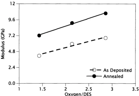
The effect of varying the 02 to DES flow rate ratio has significant effect on the film properties. The O2:DES ratio was changed from 10:7 to 15:7 to 20:7 while holding all other variables constant. Increasing this ratio caused the deposition rates to increase proportionally, rising from 65.2 to 73.6 to 89.7 nm/min, with standard deviations below 1.5 nm/min. Both hardness and modulus increased significantly with increased oxygen flow rate, as shown in Figure 2-5 and Figure 2-6. The higher percentage of 02 in the gas feed results in greater incorporation of oxygen into the film structure and thereby creates a more cross-linked material. Again, there is a significant jump in the mechanical properties upon annealing due to the condensation reaction that occurs between proximal -OH end groups. A slight decrease in index of refraction can be seen with increased oxygen flow, with values around 1.44. After annealing, the index of refraction drops into the
1.42-1.43 range. n 1.6- 0-U 1.2-v, C -
0.8-I
0.4- 0.0-I 1.5 2 2.5 3 3.5 Oxygen/DESFigure 2-5: Effect of precursor flow rate ratios on hardness. A0 -©
--- As Deposited
*- Annealed
12 9.6 -U
7.2--
0 4.82.4 0.0 -1 1.5 2 2.5 3 3.5 Oxygen/ DESFigure 2-6: Effect of precursor flow rate ratios on elastic modulus.
2.5.2 PLASMA PROCESSING CONDITIONS
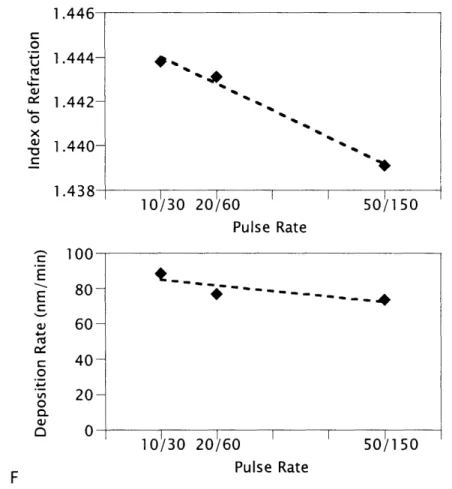
Pulsed plasma enhanced CVD is a commonly used method to further tune the film properties and is accomplished by turning the plasma off and on in set intervals.3 0'3 4'3 5 This method of plasma deposition proved less problematic, as it was observed that pulsing reduced particle generation in this work. The pulse rate was changed, while holding the duty cycle (plasma on time / total cycle time) constant at 25%. The peak power remained constant at 200 W, allowing the equivalent power (duty cycle * peak power) to remain fixed at 25 W. The resulting deposition rates and indices of refraction are shown in Figure 2-7. The index of refraction increases with shorter on/off-times (i.e. 10/30) representing an increase in the dielectric constant. However, this also leads to a higher deposition rate.
-0
0O
~
~
__
--e- As Deposited ---Annealed
I I I I11--*
10130 20/60
Pulse Rate
10/30 2060 I I
501150
Pulse Rate
Figure 2-7: Refractive indices and deposition rates versus plasma pulsing conditions.
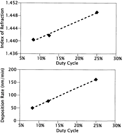
The duty cycle was also varied while maintaining a constant equivalent power, and the results are shown in Figure 2-8. A higher duty cycle results in higher indices of refraction as well as higher depositions rates.
1.1-Tr 1u *".v w. C 0 4--J t-CU I.. cc O X x ¢) - 1.444- 1.442- 1.440- 1.438-50/150 ,vv 80- 60- 40- 20-C E E +-C 4-/ c, O .aO
---
_
F aaZ A r -. A\ A\ _ I I Jl I I U1 A ) I t1') 0 *' 1.448-U fu 4-"" 1.444-4-0 x -v
1.440- 1.436-E E 150- c-a 100-- 50-ao 0- --5% 10% 15% 20% 25% 30% Duty Cycle -n _^ 5% 10% 15% 20% 25% 30% Duty CycleFigure 2-8: Refractive Indices and Deposition rates versus duty cycle
2.6 CONCLUSIONS
OSG thin films were deposited using diethylsilane and oxygen via pulsed-PECVD. The FTIR spectrum confirmed significant organic content (CH2, CH3) as well
as a considerable hydroxyl inclusion from water impurities. Although diethylsilane was the chosen precursor due to the higher organic content that its methyl silane counterparts, the high organic content can ultimately be the limiting factor with DES if carbon bridging occurs and silicon carbide formation begins. Upon annealing at 400 C, the hydroxyl groups were removed and intensity of the primary Si-O-Si stretch at 1060 cm-' increased, indicating a condensation reaction
is occurring between proximal hydroxyl end groups resulting in a more crosslinked
_ I I I I 'p. .p .V~~~~~~~~' *~~~~~~~ PP I1 _ I I I I
material. The loss of hydroxyl end groups as well as the decrease in density caused by the condensation resulted in a lower index of refraction post annealing. The increased degree of crosslinking also coincided with improved mechanical properties as seen in other works. In some instances, the hardness more than doubled and the modulus increased by over 50% after annealing. All films showed a modulus of 4.0 GPa or greater, indicating mechanical integrity would remain intact for a standard oxide CMP process.3 6
Recently, Burkey's work detailing structural and mechanical properties of OSG materials that employing a similar condensation reaction was reported.30 Similar structural changes were observed with FTIR however the hardness mostly increased (-6 to 20%) with post-anneal, obtaining a maximum hardness observed
0.527 GPa. However, the increase in modulus detailed in this work was not observed. Indices of refraction ranged from 1.469 to 1.475 for the as-deposited materials and fell to 1.423 to 1.454 for the annealed, a more dramatic decrease than was observed.
Similar OSG materials have been previously produced by CVD using different precursors. Grill and Patel produced low-k materials from tetramethylsilane with indices of refraction ranging from 1.47 to 1.80 and corresponding dielectric constants from 3.0 to 4.5.37 Pang et al. reported properties for Black Diamond, a silicon dioxide-like material, having a dielectric constant of 2.5 and index of refraction at 1.46.38
Changing the relative amounts of oxygen and DES also has a substantial impact on film structure. Increasing the 02/DES ratio results in greater oxygen incorporation into the film structure, which leads to harder, more crosslinked films. Additionally, both increasing the duty cycle and decreasing the pulse rate results in a denser film with a higher refractive index as well as higher deposition rates. By adjusting these processing parameters, films can be systematically tuned to have
its specific properties; however, there is often a give-and-take between achieving a lower index of refraction and obtaining higher deposition rates.
REFERENCES
1. M. B. Anand, M. Yamada, and H. Shibata, IEEE Trans. Electron Devices 44, 1965 (1997).
2. M. ONeill, A. Lukas, R. Vrtis, J. Vincent, B. Peterson, M. Bitner, and E. Karwacki,
Semiconductor International (June 2002).
3. D. Thomas, Y. Song, and K. Powell, SolidState Technol. 44, 107 (2001).
4. M. Morgen, E. T. Ryan, C. H. Jie-Jua Hua, T. Cho, and P. S. Ho, Annu. Rev. of Mater. Sci. 30, 645 (2000).
5. A. Grill, J. Appl. Phys. 93, 1785 (2003).
6. E. S. Lopata, L. Young, andJ. T. Felts, Mater. Res. Soc. Symp. Proc. 612, D5.3.1 (2000).
7. M. J. Loboda, Microelectron. Eng. 50, 1 5 (2000).
8. A. Grill and V. Patel, Appl. Phys. Lett. 79, 803 (2001). 9. A. S. Brown, IEEESpectrum 40, 36 (2003).
10. L. Peters, Semiconductor International(May 2002).
11. R. D'Agostino, Plasma deposition, treatment, and etching of polymers (Academic Press, Boston, 1 990).
12. R. A. Levy, L. Chen, J. M. Grow, and Y. Yu, Mater. Lett. 54, 102 (2002). 13. R. A. Levy, J. M. Grow, and G. S. Chakravarthy, Chem. Mat. 5, 1710 (1993). 14. J. M. Grow, R. A. Levy, Y. T. Shi, and R. L. Pfeffer,J. Electrochem. Soc. 140, 851
(1993).
15. R. A. Levy and J. M. Grow, Mater. Sci. Eng. B-Solid State Mater. Adv. Technol. 1 7, 1 72 (1993).
16. J. D. Patterson and M. C. Ozturk,J. Vac. Sci. TechnoL. B10, 625 (1992).
17. S. M. George, P. A. Coon, M. L. Wise, A. C. Dillon, and M. B. Robinson, Abstr. Pap.
Am. Chem. Soc. 202, 8 (1991).
18. P. A. Coon, M. L. Wise, A. C. Dillon, M. B. Robinson, and S. M. George,J. Vac. Sci. Technol. B10, 221 (1992).
19. D. T. C. Huo, M. F. Yan, and P. D. Foo, J. Vac. Sci. Technol. A 9, 2602 (1991).
20. K. Usami, S. Sugahara, M. Kobayashi, K. Sumimura, T. Hattori, and M. Matsumura, J.
Non-Cryst. Solids 260, 199 (1999).
21. Q. G. Wu and K. K. Gleason, J. Vac. Sci. Technol. A 21, 388 (2003).
22. R. F. Cook, E. G. Liniger, D. P. Klaus, E. E. Simonyi, and S. A. Cohen, Mater. Res. Soc.
Symp. Proc. 511, 33 (1998).
23. L. H. Lee, W. C. Chen, and W. C. Liu, J. Polym. Sci. Pol. Chem. 40, 1560 (2002).
24. H. C. Liou and J. Pretzer, Thin Solid Films 335, 186 (1998).
25. A. M. Padovani, L. Rhodes, S. A. B. Allen, and P. A. Kohl,J. Electrochem. Soc. 149, F161 (2002).
27. H. G. Tomkins and W. A. McGahan, Spectroscopic Ellipsometry and Reflectometry: A
User's Guide (Wiley-lnterscience, New York, 1 999).
28. J. H. Mulvey, The Nature of Matter(Oxford University Press, New York, 1 981). 29. C. J. F. Bottcher, O. C. van Belle, P. Bordewijk, and A. Rip, Theory of Electric
Polarization, 2nd ed (Elsevier Scientific Pub. Co., New York, 1973).
30. D. D. Burkey and K. K. Gleason, J. Appl. Phys. 93, 5143 (2003).
31. B. C. Bunker, D. R. Tallant, T. J. Headley, G. L. Turner, and R. J. Kirkpatrick, Phys. Chem. Glasses 29, 106 (1988).
32. A. J. Moulson and J. P. Roberts, Trans. FaradaySoc. 57, 1208 (1 961).
33. D. H. Levy, K. K. Gleason, M. Rothschild, J. H. C. Sedlacek, and R. Takke, Appl. Phys.
Lett. 60, 1667 (1 992).
34. H. Yasuda and T. Hsu, J. Polym. Sci., Polym. Chem. Ed. 15, 81 (1977).
35. Y. Wu, L. Han, B. Thomes, H. Qiu, C. Savage, W. Lee, and R. Timmons, Mater. Res. Soc. Symp. Proc. 544, 77 (1999).
36. E. T. Ryan, S. Lin, D. Nelsen, J. T. Wetzel, D. Gidley, and J. Drage, Advanced
Metallization Conference 2001, Proceedings of the Conference (Pittsburgh, 2001),
557.
37. A. Grill and V. Patel,J. AppL. Phys. 85, 3314 (1999).
CHAPTER THREE
EFFECTS OF CONDENSATION REACTIONS ON THE
STRUCTURAL, MECHANICAL, AND ELECTRICAL
PROPERTIES OF PLASMA-DEPOSITED ORGANOSILICON THIN FILMS FROM OCTAMETHYLCYCLOTETRASILOXANE
ABSTRACT
Organosilicon thin films were deposited from octamethylcyclotetrasiloxane and hydrogen peroxide using pulsed-plasma enhanced chemical vapor deposition. FTIR analysis shows significant organic content as well as hydroxyl and silanol moieties present in the as-deposited materials. Complete removal of the hydroxyl groups after annealing at 400 C for 1 hour was confirmed by FTIR and indicates that a condensation reaction between proximal hydroxyl groups occurs. This leads to the formation of additional Si-O-Si linkages, also confirmed by FTIR, and these structural changes lead to increased mechanical properties for the film. Mechanical property measurements were in accordance with this hypothesis, as the hardness increased between 46 and 125% after annealing. The structure-hardness relationship was evaluated in the framework of the continuous random network theory and a percolation of rigidity was observed at a connectivity number of
2.35-2.4. Dielectric constant of the annealed films ranged between and 2.78 and 3.20. Film structure and properties were strongly dependent on the feed rate of the
3.1 INTRODUCTION
As feature sizes for integrated circuits continue to shrink, the semiconductor industry is focusing technology to minimize the intrinsic time delay for signal propagation, quantified by the RC delay. One avenue for reduction in the RC delay is to lower the capacitance, C, between the wires by decreasing the dielectric constant, k.' One important class of low-k materials is the carbon-doped silicon oxides, also known as organosilicate glasses (OSGs).2'3 The Si-C bonds in OSGs are more covalent in nature than the Si-O bonds, since Si and O have a large electronegativity difference giving ionic character to their bonds leading to increased polarizability and hence higher dielectric constants.4 Furthermore, OSG materials have been examined for their ability to create pseudo-porosity by loosening the dense, crosslinked SiO2 lattice, as a proportion of the Si-O bonds are terminated by methyl groups bound to Si atoms.5 Additionally, heavier Si and O atoms are replaced with lighter C and H atoms resulting in a reduction in the film density, decreasing the k-value.3 4 Today, dense OSG thin films generally yield
dielectric constants ranging from 2.4 to 3.3.6- 9
Chemical vapor deposition (CVD) is a commonly used deposition technique in semiconductor manufacturing.' 0 CVD utilizes gas phase chemistries in a low to ultra-low pressure environment to produce well-defined, high quality films in a controllable and tunable fashion." In this work, OSG thin films were created from octamethylcyclotetrasiloxane (D4), a cyclic organosilcon, and a hydrogen peroxide solution, which is used as an oxidant . The D4 precursor has previously been used
to produce SiO2-based thin films using a plasma-enhanced CVD,12 pyrolytic
CVD,1'3 '4 and pulse-modulated microwave ECR.'5 D
4 is advantageous as it
content (Si-CH3), unlike the silane precursors often used, which lack any Si-O bonds.
The successful integration of OSG films in advance microelectronic devices is dependent on the improvement of their mechanical properties.'6 The addition of organics to the silicon dioxide lattice reduces the network bonding and results in a more open structure with a reduced density. This results in reduced mechanical properties and creates issues with latter processing steps, such as the ability to survive chemical-mechanical polishing.2" 6 Spin-on deposition, another technique sometimes used for low-k materials, relies on a thermal curing step that leads to a structural transformation which supplies the material's strength.'7-2' Often utilizing alcohol or water condensation chemistry, reactions between proximal end groups help to crosslink the film, thereby making it mechanically robust. Burkey recently extended this concept to CVD processes by using a water oxidant during deposition.2 2' 23 This work further explores the ability of condensation chemistry to improve the mechanical properties of CVD OSG films by using hydrogen peroxide as the oxidant during deposition. Hydrogen Peroxide has several foreseeable advantages over water. First, each molecule can produce two hydroxyl groups while each water molecule can generate only one. Additionally, the H-OH bond in water has a high bond dissociation energy of 11 8 kcal,24 while the HO-OH bond in hydrogen peroxide has a much lower dissociation energy of 51 kcal,2 5 making it easier to break. Water is also more likely to produce hydrogen radicals which can lead to the formation of Si-H bonds which are undesirable due to their higher polarizability,2 6 which leads to higher dielectric constants, as well as their high reactivity which can also cause difficulties during later processing steps.27
3.2 EXPERIMENTAL
Depositions were carried out in a custom-built, parallel-plate vacuum chamber described elsewhere.2 8 The PECVD system has an upper electrode powered by a 13.56 MHz RF source with attached matching network and a grounded lower electrode. The lower electrode also functions as the substrate stage and was kept at room temperature using a water cooled system. In addition, electrostatic clamping capabilities were utilized to help maintain constant substrate temperatures. The substrates used were 100 mm diameter silicon wafers. The upper electrode / shower-head distributes all incoming precursor gases over the substrate. Octamethylcyclotetrasiloxane (D4, Gelest Inc., CAS 556-67-2, 98%) was
the monomer used with no further purification and hydrogen peroxide (H202, Sigma
Aldrich, 50% aqueous solution, CAS 7722-84-1) was used as an oxidant. Both the D4 and oxidant were volatilized in a glass jars and delivered to the reactor chamber through a calibrated needle valves. For all depositions, chamber pressure was
maintained at approximately 300 mTorr and is controlled by a butterfly valve connected to an MKS model 252A exhaust valve controller. When investigating thermal stability, films were annealed at 400 °C and ambient pressure in a nitrogen atmosphere for one hour.
Fourier Transform Infrared (FTIR) Spectroscopy was performed on a Thermo Nicolet Nexus 870 ESP spectrometer in transmission mode at 4 cm-' resolution using 64 scan averaging. A 10 minute nitrogen purge was performed between each measurement to diminish the effects of carbon dioxide and moisture. All spectra were baseline corrected and had their intensity normalized to a thickness of 5000 A
using their measured thicknesses and Beer's Law.
Film thicknesses and indices of refraction (n633) were determined using VASE, Variable angle spectroscopic ellipsometry, performed on A Woolam M-2000