HAL Id: hal-02324322
https://hal.archives-ouvertes.fr/hal-02324322
Submitted on 1 Nov 2019
HAL is a multi-disciplinary open access
archive for the deposit and dissemination of
sci-entific research documents, whether they are
pub-lished or not. The documents may come from
teaching and research institutions in France or
abroad, or from public or private research centers.
L’archive ouverte pluridisciplinaire HAL, est
destinée au dépôt et à la diffusion de documents
scientifiques de niveau recherche, publiés ou non,
émanant des établissements d’enseignement et de
recherche français ou étrangers, des laboratoires
publics ou privés.
Interface tailoring for charge injection control in
polyethylene
G. Teyssedre, S. Li, K Makasheva, N. Zhao, Laurent Millière, Christian
Laurent
To cite this version:
G. Teyssedre, S. Li, K Makasheva, N. Zhao, Laurent Millière, et al.. Interface tailoring for charge
injection control in polyethylene. IEEE Transactions on Dielectrics and Electrical Insulation, Institute
of Electrical and Electronics Engineers, 2017, 24 (3), pp.1319-1330. �10.1109/TDEI.2017.006142�.
�hal-02324322�
Interface Tailoring for Charge Injection Control
in Polyethylene
G. Teyssedre
1, S.T. Li
2, K. Makasheva
1, N. Zhao
2, L. Milliere
1andC. Laurent
11 LAPLACE (Laboratoire Plasma et Conversion d’Energie), Université de Toulouse CNRS, INPT, UPS, Bat 3R3, 118 route de Narbonne, F-31062 Toulouse Cedex 9, France 2 State Key Laboratory of Electrical Insulation and Power Equipment, School of Electrical Engineering
Xi’an Jiaotong University, Xi'an, Shaanxi, 710049, China
ABSTRACT
The insulating materials used to develop HVDC technologies suffer from a major drawback, which is the accumulation of electrical charges forming internal space charge with possibly two major consequences: (i)- the out-of-control of the internal electric field distribution initiating current runaway and (ii)- cumulated molecular level damages extending or creating defects and leading ultimately to breakdown. To prevent space charge accumulation, one possible route, not examined in depth by the scientific community to date is to control the charge injection at the interfaces between the insulating material and the “electrodes” (metallic or semi-conducting). Different routes were followed in this work for tailoring the interface between electrode and polyethylene material, based on chemical modification of the insulation or layer intercalation. Depending on the process, charge injection control is achieved either for negative charges or for charges of both polarities. The process of charge injection control is discussed with reference to the chemical/physical modifications brought about by the different treatments. The results provide indication towards a strategy to control the injection in power cables and other electrical components.
Index Terms — HVDC insulation, space charge, tailoring interfaces, charge injection
mitigation.
1
INTRODUCTION
E
LECTRICAL insulating polymers are among key issues in the development of HVDC systems. They are found as insulation or dielectric in a variety of components and systems, such as cables, capacitors, electrical machines, converters, etc. The main advantages of such materials are their thermo-electrical and mechanical properties, the possibility to be recycled, and the maintenance costs they confer to the systems in which they are included (vs. liquid insulation for example). However, they suffer from a major drawback. It is the accumulation of electrical charges forming internal space charge under HVDC conditions with possibly two major consequences: (i)- the internal electric field distribution is not anymore the design field. It represents a risk of formation of local domains where the higher field values can initiate current runaway of thermal or electrical origins eventually leading to dielectric breakdown [1, 2], and (ii)- by cumulated local damages to the structure of the dielectric at a molecular level. Local defects can be extended up to the stage where electrical discharges and electrical treeing can appear leading ultimately to breakdown [3-5]. Both consequences induce a loss of system reliability. Being part of larger power systems, a local breakdown in one of the system constituentscan give rise to much larger consequences (for example, dielectric breakdown of the insulation of a power electrical cable led to the blackout of part of the European grid in November 2006; similar accidents happened in the USA). Preventing the formation of space charge in insulation is therefore a necessary step to enhance system reliability, allowing a higher level of integration of power systems with the associated gain in terms of environment and space saving. This would strengthen the development and provide a firm basis for emerging HVDC technologies.
Space charge in insulating materials originates from charge injection at the contact between conductive (or semi-conductive) parts with the insulation and from internal dissociation of weakly bounded species. In high quality electrical insulation used for HVDC systems, and specially cross-linked polyethylene used for the insulation of HVDC cables, the presence of cross-linked by-products is refrained by improved physical and chemical cleanliness of materials [6]. With these improvements it can be anticipated that the internal dissociation becomes a secondary factor when compared to charge injection for space charge generation as it is for Low Density Polyethylene –LDPE- the base resin of XLPE. Controlling charge injection would therefore give a striking advantage in terms of insulating properties and
Manuscript submitted on 1July 2016, in final form 26 September 2016, accepted 16 October 2016. Corresponding author: G. Teyssedre.
reliability of the insulated system.
Understanding space charge in insulating polymers has been the subject of a strong activity in the international community within the last 30 years [7, 8]. With the refinement of the measurement techniques charge build-up can be followed under DC and AC stress with a spatial resolution of the order of 10 µm for the conventional technique and a time resolution of less than the millisecond [9]. In the light of the knowledge obtained by using these techniques, several groups tried to tailor material properties in order to control the internal space charge. These attempts more often concern the bulk properties of materials. For example, and because atomistic modelling allows the estimation of the trap depths due to chemical species introduced into the structure of polyethylene [10, 11], researches focus on chemically doping of the polymer for HVDC applications [12]. Later researches focus on nanocomposite materials, with as goal to reduce space charge build-up in existing matrices, and/or to provide materials with relevant thermo-mechanical properties avoiding the crosslinking step [13-15]. Among these approaches, some studies focus on the interface properties between a semi-conducting layer –semicon– and the extruded polymer because it is the structure of HVDC power cables. Efforts were devoted to avoid field intensification at the interface due to the surface roughness of the semicon. HVDC grade semicon was developed using a specific quality of carbon black with less ionic impurities and with percolated structure [16].
Very few studies focus on the interface properties to change its characteristics in terms of charge trapping probably because in a general way the phenomena at play are complex and not correctly described. At the same time, it is recognized that charge build up [17, 18] and even conductivity measurements [19, 20] heavily depend on electrode conditions of samples and not only on bulk properties of insulations. Two routes can be envisaged for modifying the injection ability of interfaces. The first one is to bring directly a modification of the insulation over a given depth by chemical treatment. The most investigated process, particularly over the last years is that consisting in fluorinating the surface of the polymer, with some success regarding space charge limitation [21, 22]. Early works have dealt with treatment of the surface using milder processes, with either oxygen, nitrogen or argon plasma [23, 24] which demonstrated some capability in lowering charge build-up. In this work we propose different conditions of fluorination and oxy-fluorination of the surface of the polymer.
The second way is to interpose a layer with controlled properties between the HV electrodes and the insulating material. This has been done by inserting thin polymer foils of various nature acting as blocking layers [25-28], or, in a more seldom way, by growing a layer by physicochemical process: hybrid polymer/silica layers act as partially-blocking electrode for charge injection in XLPE [29]. We will consider the route consisting in interposing a thick interface layer made of a dielectric nanocomposite and that consisting in depositing artificial deep traps with metallic nanoparticles embedded in a thin plasma processed matrix. In the next section, the rationale of each of the three processes and its implementation are described.
2 PROCESSES FOR INTERFACE
TAILORING
Different interface modifications have been implemented to the same kind of insulation, being low density polyethylene, so as to be in situation where electronic carriers dominate charge build-up [30]. LDPE substrates were press-molded into films of typically 300 µm thickness and 80 mm diameter. The efficiency of the interface processing was analyzed through its impact on injection phenomena comparatively to reference untreated LDPE. Assessment of the efficiency in charge injection mitigation was achieved through a main means consisting in space charge measurements in all instances, using similar protocols. Depending on the treatment used, different physicochemical techniques were implemented to characterize the modifications being operated. We first describe the different interface tailoring methods and the rationale for applying them.
Features of the implemented three surface modification processes are summarized in Table 1 and described below. Two of them consider the addition of an interface layer being either a thick interface (10-100 µm) made of high permittivity nanoparticles-containing polymer or a thin one (less than 100 nm), with a silver nanoparticles-containing organosilicon layer deposited by plasma process. The last method consisting in chemically modifying the LDPE matrix by chemical attack leads to an intermediate thickness treated layer (2 µm). The methods have in common to target charge trapping at the interface, hence reduction of the electric field at the interface.
Table 1. Principle and reasoning for the different methods addressed for
charge build-up mitigation.
Treatment type Process outline Reasoning
Grafting of polar groups
Chemical grafting of oxygen/fluorine atoms at the polyethylene surface by exposure to F2/O2 gas mixture.
Polar groups are likely to produce deep traps for electrical charges
Thick nanocomposite layer
Interposition of a ≈30µm thick
nano-composite made of BaTiO3
or TiO2 NPs and LDPE matrix
by hot pressing
Charge stabilization owing to the high permittivity / high polarizability of NPs Thin nanocomposite layer
Thin organosilicon dielectric layer deposition by plasma process incorporating a plane of non-percolating silver nanoparticles at controlled distance from the surface
Silver NPs owing to their ability to store positive or negative charges would act as deep traps for electrical charges
2.1 (OXY-) FLUORINATION
2.1.1 BACKGROUND AND PRINCIPLE
Among surface treatment approaches for preventing charge injection, modification or intercalation of polymer was attempted. Hence, LDPE modified with carbonyl groups (LDPE-α) [25], polyvinyl fluoride (PVF) [26], polyethylene terephthalate (PET) [27] or fluorinated ethylene propylene copolymer (FEP) [28], were inserted between electrode and
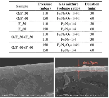
Table 2. Parameters of oxy-fluorination and fluorination processes. All
treatments were achieved at 25°C.
Sample Pressure (mbar) Gas mixture (volume ratio) Duration (min) O/F_30 110 F2/N2/O2=1/4/1 30 O/F_60 150 F2/N2/O2=1/4/1 60 F_30 110 F2/N2=1/4 30 F_60 150 F2/N2=1/4 60 O/F_30+F_30 110 F2/N2/O2=1/4/1 30 110 F2/N2=1/4 30 O/F_60+F_60 150 F2/N2/O2=1/4/1 60 150 F2/N2=1/4 60
Figure 1. Cross-section view by SEM of reference (left) and
oxy-fluorinated (right) LDPE.
d=1.7µm
polymer to suppress charge injection. Also, some works were introduced with modification of the polymer surface with oxygen/nitrogen plasma with few reports addressing the impact of the surface treatment on space charge and/or charge injection [23]. The above approaches have all in common to introduce polar groups at the surface of the material, likely to stabilize charges. Fluorination and oxy-fluorination belong to that family in the sense that electronegative atoms are grafted to the polymer. The process consists in exposing the polymeric material to a F2/O2 gas mixture and is one of the most effective approaches to enhance the adhesion properties of polymers (especially polyolefins). It has been widely developed from fundamental researches to industrial applications in chemical industry, just like direct fluorination which is mostly used to improve the barrier properties, separation properties, chemical stability and biocompatibility. The combination of strongly increased surface layer permittivity and deep charge traps in the treated interface system is thought as responsible for the mitigation of charge injection of the fluorinated [21] or oxy-fluorinated [22] samples.
2.1.2 OPERATING CONDITIONS
The processed samples are thin films of LDPE (Borealis LE4147) about 280 μm in thickness, obtained by hot-pressing bare LDPE pellets for 10 min, at 135 °C under a pressure of 10 MPa. Three process schemes: oxy-fluorination (labeled as O/F_30 and O/F_60), fluorination (F_30 and F_60) and oxy-fluorination followed by oxy-fluorination (O/F_30+F_30 and O/F_60+F_60) were implemented for tailoring the LDPE interface. Process parameters are indicated in Table 2. The process temperature was set to 25 °C and the gas mixtures used were F2/N2/O2 = 1/4/1 and F2/N2 = 1/4 in volume. For comparison, the process duration and total pressure of the three process schemes were selected as 30 min, 110 mbar and 60 min, 150 mbar. All the processes were conducted in a stainless steel reactor with convection equipment. Prior and after the process, the reactor was three times washed with dry N2. The reactive gas was expelled into absorption system.
The processes form a oxy-fluorinated/fluorinated layer on both sides of the LDPE samples, the morphology as shown in the cross-section view by SEM in Figure 1. The thickness of the oxy-fluorinated/fluorinated layer varies from about 0.1 µm to several microns depending on process conditions. Space charge mesurements were carried out using the pulsed electroacoustic –PEA- technique with semicon electrode on anode side and Aluminum on cathode side. Before starting PEA tests, samples were thermally treated at 60 °C for 48 hours to exclude the influence of water and some volatile impurities. The chemical component of the oxy-fluorinated/fluorinated layer was also tested by X-ray photoelectron spectroscopy (XPS, AXIS ULtrabld, Kratos).
2.2 THICK NANOCOMPOSITE LAYER INTERCALATION
2.2.1 BACKGROUND AND PRINCIPLE
Nanodielectrics were firstly reported by Lewis in 1994 [31]. Dispersion of nanoparticles into polymer matrixes has then proved to be very effective in suppressing space charge
build-up [32-37]. As examples, nanometer-size fillers of silica (SiO2) [38] and magnesium oxide (MgO) [13] incorporated into LDPE have been shown to be effective in suppressing space charge. Though the mechanisms behind these improvements are not completely clear at present [14, 15, 39], an interpretation based on deep trap formation at the interface between LDPE and MgO nanoparticles was put forward by Takada et al. [35, 40]. This was substantiated by thermally stimulated depolarization current (TSDC) measurements and conductivity [41, 42]. Beyond the classical implementation of nanocomposites as bulk insulation, our purpose in this work was to use it as a thick interface layer with incorporating nanoparticles of high permittivity. The objective here is twofold: on the one hand, owing to their high permittivity, particles would act as deep traps for charges. In the field of organic semiconductors, it is recognized that high-k dielectrics produce carrier localization enhancement and charge formation at the interface between the dielectric and semiconductor material of organic field emission transistors (OFETs) [43, 44]. On the other hand, the interface layer would decrease the field in the higher permittivity part of the material, i.e. at the interface with electrodes, which is considered as constituting the weak region of the material. So far only very scarce works concern space charge characteristics of nanocomposite/polymer multilayers [45, 46].
2.2.2 OPERATING CONDITIONS
Sample processing conditions are available elsewhere [46]. Titanium oxide nanoparticles (nTiO2) with diameter 20±5 nm were selected and surface treated by using silane coupling agent. They were dispersed into the LDPE material with five different concentrations, from 0.5 to 10 phr (parts per hundred parts of resin) using a torque rheometer (R-90-200, Germany) at 135 °C for 30 min at 50 rpm. Dispersion of the nanoparticles was monitored by SEM. Fairly well dispersed materials were obtained [46]. The bare LDPE and the TiO2
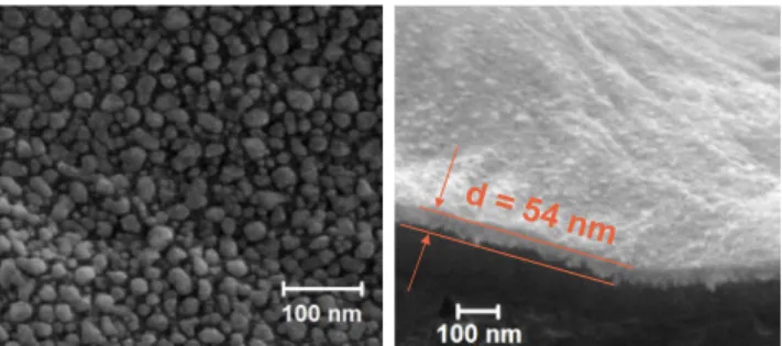
-Figure 2. Left: SEM image of the AgNPs layer deposited on LDPE
substrate; Right: SEM cross-section of the AgNPs/SiOxCy:H stack on
LDPE substrate.
LDPE nanocomposite materials were press-molded into thin films at 140 °C, with thicknesses of 140 or 60 µm, the thickest films being used as central layer in the three-layer stacks. Films were further co-pressed into bilayers or three-layers of about 250 µm thickness, under a pressure of 10 MPa at 80 °C for 20 min.
Before space charge measurements, samples were thermally treated as described above. Complementary measurements as conductivity under 30 kV/mm and permittivity were realized as detailed in [42]. TSDC measurements were achieved using a commercial test system (Concept 90, Germany), with polarizing temperature of 70 °C, field of 4 kV/mm for 20 min. After cooling under field, current was recorded from -100 °C to 90 °C at a rate of 3 °C/min.
2.3 PLASMA-PROCESSED THIN NANOCOMPOSITE
2.3.1 BACKGROUND AND PRINCIPLE
It is recognized that charge injection in insulating materials does not consist for charges in passing over the energetic barrier from the metal into a perfect wide band gap material [47]. In polyethylene, this barrier would be around 4 eV. With this value, the injection current derived from the classical injection law, Schottky and Fowler-Nordheim [48], would be virtually zero at the field and temperature where injected charges are being detected in insulating polymers. Modelling work as well as experiments [47], point to apparent injection barrier of 1 eV or so. A recent modelling work to explain the electroluminescence at the metal/polymer contact [49] indicates that a more appropriate interface description is to consider an exponential distribution in the density of trapping sites from band edges into the gap. Atomistic modelling has shown that this description [50] is consistent with the existence of chemical traps (forming the deepest levels) and physical traps (forming the shallowest levels). One possible route for preventing charge build-up consists in forming deep traps at the interface in such a way to permanently trap the injected charges. This would have two effects: on one hand, the trapped charges would induce a counter field which would moderate the injecting field at the electrode thereby reducing further injection and on the other hand these charges would not be available anymore for transport. A rough estimation shows that, in order to reduce the field at the contact, typically by about 10 kV/mm as order of magnitude of applied field, a trap density of 6×1011 cm-2 is needed, representing an inter-particle distance of 13 nm if each inter-particle holds one charge. In order to do so, we have processed a thin dielectric layer containing a single layer of silver nanoparticles -AgNPs [51, 52]. By their metallic nature, the AgNPs would stabilize the injected charges and the distance between the electrode and the plan of the silver nano-grains would allow an efficient capture of the injected electrons. The sputtered silver nanoclusters are then embedded into an organosilicon matrix.
2.3.2 OPERATING CONDITIONS
The nanocomposite layer used for tailoring LDPE interfaces consists of AgNPs/SiOxCy:H stack. The deposition was performed in two-steps process: silver sputtering to obtain the single layer of AgNPs followed by plasma polymerization to create the dielectric cover matrix [53]. Control of the plasma
parameters allows strict control over the size and density of the AgNPs in the dielectric matrix. For both steps, we have used an axially-asymmetric RF (13.56 MHz) capacitively-coupled discharge maintained at low gas pressure [54]. The results given in this work are for sputtering time of 5 s for a plasma maintained in pure argon at pressure of p = 8.0 Pa with RF power of P = 40 W which induces a self-bias voltage of Vdc = -725 V on the powered (smaller) electrode to perform the sputtering. The processed dielectric layer to cover the AgNPs is a plasma organosilicon deposit (SiOxCy:H) obtained in the same reactor with argon-hexamethyldisiloxane (HMDSO, [CH3]6Si2O) mixture at total gas pressures of ptot = 6.6 Pa and input power of P = 80 W (Vdc = -900 V).
Using these plasma conditions, large and isolated AgNPs, of 15 nm of average size and surface density of 6.1×1011 cm-2 are deposited, cf. Figure 2. Then they are embedded in an organosilicon matrix with insulating properties to form the nanocomposite stack of 50 nm total thickness. Details on the structural characterization of the obtained nanocomposites and the relation between plasma parameters and AgNPs features are given elsewhere [51, 55].
Additive-free LDPE substrates, 300 μm in thickness and 70 mm in diameter, were processed by press-molding. Either one or the two faces of the LDPE sample were tailored with identical nanocomposite layers. Prior to measurement, bare LDPE was submitted to the same vacuum conditioning as for the sample with processed nanocomposite layers in order to make the comparison with equal outgassing degree.
2.4 ASSESSMENT METHODOLOGY
The capability of processes to mitigate charge injection has been evaluated mainly by space charge measurements. This can be considered as an indirect method to probe injection since charges have to drift in the bulk on a distance larger than the spatial resolution of the measurement set-up to be clearly revealed. At the same time, it enables to localize and distinguish the type of carriers, whereas charging current for example may result from different contributing processes and is more ambiguous to interpret. We will show later on that conduction current support the injection mitigation effect observed by space charge measurements. All space charge measurements were carried out using the pulsed electroacoustic –PEA- method, using facilities available at partner's sites [55, 56]. Approaching experimental procedures were adopted throughout the work for assessing the different tailoring methods. In particular, PEA measurements were
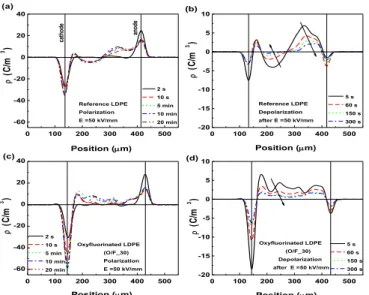
Figure 3. Space charge density profiles of (a) reference LDPE at
polarization E=50 kV/mm, (b) reference LDPE at depolarization after
E=50 kV/mm, (c) oxy-fluorinated LDPE at polarization E=50 kV/mm
and (d) oxy-fluorinated LDPE at depolarization after E=50 kV/mm. 0 100 200 300 400 500 -60 -40 -20 0 20 40 an od e (C/m 3 ) (C/m 3 ) (C/m 3) (d) (c) (b) Reference LDPE Polarization E =50 kV/mm (C/m 3 ) 2 s 10 s 5 min 10 min 20 min ca th od e (a) 0 100 200 300 400 500 -20 -15 -10 -5 0 5 10 Position (m) Reference LDPE Depolarization after E =50 kV/mm 5 s 60 s 150 s 300 s Position (m) 0 100 200 300 400 500 -60 -40 -20 0 20 40 Oxyfluorinated LDPE (O/F_30) Polarization E =50 kV/mm 2 s 10 s 5 min 10 min 20 min Position (m) 0 100 200 300 400 500 -20 -15 -10 -5 0 5 10 Oxyfluorinated LDPE (O/F_30) Depolarization after E =50 kV/mm 5 s 60 s 150 s 300 s Position (m)
Figure 4. Average space charge density as a function of process scheme
in different process conditions (depolarization for 5 s after polarization for 20 min under 30 kV/mm).
0.0 1.0 2.0 3.0 O/F+F F O/F untreated LDPE 30 min, 110 mbar 60 min, 150 mbar Ave rage spa ce cha rge d e nsi ty ( C/ m 3 ) Process scheme
carried out at room temperature with relatively short charging time (typically 20 min) in order to analyze the earlier instants of charge injection into the materials, and applying fields in the range 10 to 50 kV/mm. Bare LDPE was used as reference. Sample preconditioning enabled a straight comparison of results between processed and unprocessed interfaces. Process efficiency was analyzed resorting to the quantity of generated charges along with the nature of charges being stored in respect to the electrodes.
3 RESULTS
In the following, for each of the tailoring process, the panel of processing parameter investigated is briefly reviewed along with its impact on space charge features. We focus on the most promising results obtained in each case.
3.1 (OXY-) FLUORINATION
Oxy-fluorination and fluorination processes were conducted under different conditions to tailor LDPE interface and the space charge characteristics of the processed samples were measured by using PEA method. Similar space charge profiles were obtained and, for space saving, only the space charge profiles of the oxy-fluorinated sample O/F_30 are shown in Figures 3c and 3d under polarization and depolarization. The space charge profiles of the reference LDPE are also shown in Figures 3a and 3b. It must be underlined that the samples were thermally treated but not outgassed prior to space charge measurements. This could explain the accumulation of a small amount of heterocharges near the cathode. Otherwise, it can be seen that holes and electrons are injected into the reference LDPE, forming positive and negative homocharges in the vicinity of the injecting electrodes. However, only positive space charge can be observed in the sample O/F_30, which indicates that electron injection is efficiently suppressed by oxy-fluorination but hole injection seems to be hardly influenced. The same qualitative features were observed for fluorination, with an amount of space charge less than by
oxy-fluorination, indicating the two methods may influence the space charge characteristics to different extents.
Therefore, the space charge profiles of the samples tailored by combined process (oxy-fluorination followed by fluorination, O/F_30+F_30 and O/F_60+F_60) were explored by PEA method. They have similar space charge characteristics to the samples processed by respectively oxy-fluorination and oxy-fluorination. Namely, electrons injection from the cathode is decreased while the hole injection from the anode is not suppressed. For quantitative analysis, the total space charge stored in the different samples was calculated and compared in Figure 4. Data plotted correspond to space-averaged charge density, taken in absolute value, obtained in volts-off 5 s after the end of the polarization step under 30 kV/mm. Three phenomena can be observed. First, the amount of space charge increases after oxy-fluorination or fluorination processes. Second, for the same process parameters, the total space charge in fluorinated samples is less than that in the oxy-fluorinated ones. The value in the sample processed by oxy-fluorination and fluorination combination goes on decreasing but with a smaller rate. Last, for each process scheme, the total amount of space charge increases with process strengthening (with increase in time and pressure).
To sum up, interface tailoring processes with the three schemes all have marked suppression effect on electron injection even under mild process conditions regardless of the fluorination intensity and introduction of oxygen atom. However, the hole injection cannot be suppressed by the tailoring methods and even increases with process duration and pressure increasing, resulting in an increase of total space charge. Finally, the amount of space charge in the samples processed by fluorination is less than that in the samples processed by oxy-fluorination.
3.2 NANOCOMPOSITE LAYER INTERCALATION
The space charge characteristics of the TiO2-LDPE nanocomposites (NCs) single layers with different nanoparticle concentrations were measured by PEA method. As example, the results obtained for 5 phr are shown in Figure 5a. The positive and negative space charge formed in the bare LDPE, cf. Figure 3a cannot be observed anymore, indicating that TiO2 nanoparticle doping can effectively suppress both
Table 3. Process parameters of thin film nanocomposites. Ref P (W) Self-bias Vdc (V) p Ar (Pa) AgNPs (NPs/cm²) Covered area Size (nm) S1 40 -725 8.00 6.1×10¹¹ 65% 15 ± 10 S2 40 -785 5.33 7.7×10¹¹ 64% < 10 S3 60 -850 8.00 2.0×10¹¹ 74% 22 ± 15 S4 60 -955 5.33 6.3×10¹¹ 75% 14 ± 10 S5 80 -968 8.00 1.8×10¹¹ 88% 30 ± 10 S6 80 -1025 5.33 4.4×10¹¹ 85% 21 ± 10
All samples feature isolated AgNPs except for S5 where coalescence appears.
Figure 6. Conductivity (dc) of the bare LDPE and of the TiO2-LDPE NCs with different nanoparticle concentrations under 30 kV/mm. In inset: TSDC glow curves of the samples after polarizing at 70 °C.
0 2 4 6 8 10 1 10 100 1000 -100 -80 -60 -40 -20 0 20 40 60 80 0 5 10 15 20 Nano-TiO 2 concentration (phr) Condu ctiv ity (10 -1 7 S/c m ) Temperature (°C) TSDC (p A) LDPE LDPE-TiO2 0.5phr LDPE-TiO2 1phr LDPE-TiO2 2phr LDPE-TiO2 5phr LDPE-TiO2 10phr
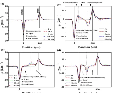
Figure 5. Space charge density profiles of (a) single layer TiO2-LDPE NC; (b) LDPE with layers of NC on each face, (c) bilayer of NC/LDPE with anode on LDPE; (d) bilayer of LDPE/NC with anode on NC. NC is LDPE with 5 phr nano-TiO2 in all cases. Applied field E=30 kV/mm.
-30 -20 -10 0 10 20
nanocomposite LDPE nanocomposite
an od e (C/m 3 ) (C/m 3 ) (C/m 3) (d) (c) (b) Nanocomposite of 2 phr Polarization E =30 kV/mm (C/m 3 ) 2 s 10 s 5 min 10 min 20 min ca th od e (a) -20 -10 0 10 240 0
Interface tailored LDPE by nano-TiO2 Polarization E =30 kV/mm 260 Position (m) 0 s 2 s 5 min 10 min 20 min Position (m) 0 -30 -20 -10 0 10 20 300 0 0 0 (-)Nanocomposite/LDPE(+) of 5 phr Polarization E =30 kV/mm 0 s 2 s 5 min 10 min 20 min Position (m) -30 -20 -10 0 10 20 (-)LDPE/Nanocomposite(+) of 5 phr Polarization E =30 kV/mm 0 300 0 s 2 s 5 min 10 min 20 min Position (m)
positive and negative space charge build-up, which is in good agreement with previous reports [57]. For analyzing the mechanism of the charge suppression, the conductivity under 30 kV/mm as well as the thermally stimulated depolarization current (TSDC) of the LDPE and NCs were tested as shown in Figure 6. It can be seen that the conductivities of the NCs are lower than that of bare LDPE, irrespective of the TiO2 content. In the TSDC glow curve of LDPE shown in inset of Figure 6, three peaks appear at about 80 °C, 53 °C and -64 °C, ascribed respectively as α (related to activity of chain elements in crystalline phase), β (related to motion of branches) and γ (related to motion of chain elements in amorphous region) relaxations [58, 59]. However, in the TSDC curve of the nanocomposites, the γ relaxation peak enhances and broadens greatly with nanoparticle concentration increasing, shifting to high temperature by about 21 °C. It actually appears as the overlying peak of two relaxation processes at about -39 °C and 2 °C proved by considering features with low NP concentration. The effect of TiO2 nanoparticle doping on γ relaxation coincides well with the research of Zhou et al. on TiO2 nanoparticle doped polypropylene [60].The nanoparticle content has not a clear trend on the α and β relaxations in the NCs with different nanoparticle concentrations.
To form intercalated interface layers, thick (≈ 60 µm) films of the LDPE / TiO2 nanocomposite, were hot pressed on both
surfaces of the LDPE film. The space charge characteristics of the interface tailored LDPE film were tested and results are shown in Figure 5b (taking the sample tailored with 5 phr NC for example). It can be seen that both negative and positive heterocharges are formed near the anode and cathode, respectively. In order to make clear the origin of these heterocharges, two-layer samples LDPE/NC were prepared by stacking thin films of LDPE and NC and using thicker NC layer in order to resolve features at the interfaces. The space charge characteristics of the samples were measured at applied electric field E=30 kV/mm, with positive voltage either set on the LDPE, namely (-)NC/LDPE(+), or on the NC, namely (-)LDPE/NC(+) -see [46, 61]. Still considering LDPE/NC samples with nanoparticle concentration of 5 phr, the space charge profiles are shown in Figures 5c and 5d, respectively. A positive space charge region is formed at the LDPE/nanocomposite polymer interface in situation (-)NC/LDPE(+), while negative space charge is formed at the polymer interface in situation (-)LDPE/NC(+). These space charge characteristics coincide well with the space charge characteristics of the interface tailored LDPE in Figure 5b, proving the heterocharges originate from dielectric/dielectric polymer interface.
3.3 PLASMA-PROCESSED NANOCOMPOSITES
The plasma operation conditions along with the results from the analysis of size, surface density and organization of sputtered AgNPs on the LDPE samples are summarized in Table 3. Three values of the input power (40, 60 and 80 W) and two values of the argon pressure (8.00 and 5.33 Pa) were used in these experiments. The self-bias voltage, related to the asymmetric nature of capacitively-coupled discharges [62], is an important parameter as it is at the origin of the acceleration of argon ions towards the silver target.
For sample S1, the AgNPs size span from 5 to 25 nm with an average size of 15 nm. Particles appear with irregular shape however, well isolated from each other. Sample S2, which has been prepared under a lower pressure (p = 5.33 Pa) for the same discharge power (P = 40 W), exhibits AgNPs of much smaller diameter (< 10 nm) with larger surface density and covered surface area of the same order as in sample S1. Sample S5 which has been prepared under the same pressure (p = 8.0 Pa) as sample S1 but for a higher discharge power
Figure 7. Space charge density versus position of (a) reference LDPE at
polarization E=50 kV/mm, (b) reference LDPE at depolarization after
E=50 kV/mm, (c) two-face tailored with AgNPs/plasma polymer stack
LDPE at polarization E= 50 kV/mm and (d) tailored LDPE at depolarization after E= 50 kV/mm. 0 100 200 300 400 -20 -10 0 10 anode 0s 5min 10min 20min 0s 5min 10min 20min ( C/ cm 3 ) Position (m) cathode Volt-on 0 100 200 300 400 -2 -1 0 1 2 Volt-off ( C/ cm 3 ) Position (m) cathode anode 0 100 200 300 400 -20 -10 0 10 Volt-on 0s 5min 10min 20min ( C/ cm 3) Position (m) cathode anode 0 100 200 300 400 -2 -1 0 1 2 (b) (a) Volt-off 0s 5min 10min 20min
Two-face tailored with S1 LDPE 50kV/mm Bare LDPE 50kV/mm ( C/ cm 3) Position (m) cathode anode (a) (b) (c) (d)
Figure 8. XPS C 1s spectra of reference and oxy-fluorination/fluorination
processed LDPE for 60min.
298 296 294 292 290 288 286 284 282 280 0 2 4 6 8 10 12 14 16 -C F 2 -C H 2 --C F 2 -C F 2 --C FH -, -C =O In te ns ity (10 4 c ps )
Binding energy (eV)
reference LDPE O/F_60 F_60 O/F_60+F_60 -C -C -, -C
H-(P = 80 W) exhibits much larger particles size spanning from 20 to 40 nm, with a covered surface area of 88%. The clusters appear coalesced with wormlike shape, a feature already reported for other type of metal clusters (gold and/or cobalt clusters) embedded in fluorocarbon [63] or hydrocarbon matrices [64]. These features of the AgNPs are in agreement with the fact that, for a given deposition time, the amount of deposited silver increases with the discharge power or the gas pressure. The above results show the capability of the plasma process to tune and control the AgNPs size and density. Considering a size of 15 nm for the AgNPs, as deduced from the SEM image of S1 in Figure 2, the NC layer can be represented by two regions with the first one consisting of a plan of AgNPs embedded in organosilicon matrix of 15 nm in thickness, and the second region of only organosilicon layer with thickness estimated to 35 nm.
Figure 7 shows the space charge patterns obtained for bare LDPE and for LDPE with two-face tailored interfaces, both in volts-on and in volts-off for 50 kV/mm of applied field. In order to make the comparison independent from test electrodes, semicon layers were used on both faces of the samples. It should also be underlined that the samples were outgassed prior to space charge measurements for volatile impurities removal. As can be seen in the pictures, positive charges appear as the dominant carriers in those conditions, consistently with experimental and modelling results reported previously [65]. Changing polarity leads to nearly symmetrical space charge patterns, with again positive space charge region forming at the positive electrode and progressively extending to the bulk of the material. In case of tailored interfaces, it can be seen that the amount of space charge is greatly reduced, with virtually no charges being accumulated in the bulk and with field profiles exhibiting no evolution with charging time
[52]. Detailed analysis of the impact of processing conditions on charge mitigation efficiency is provided elsewhere [52]. With using one-face tailored sample, it was confirmed that the treatment is efficient for both positive and negative charge injection. Already the organosilicon layer appears efficient in reducing the space charge build-up. The introduction of AgNPs to form the stack strengthens the effect, provided large and isolated particles are settled at appropriate distance from the interface.
4 DISCUSSION
4.1 MECHANISMS OF CHARGE INJECTION MITIGATION
4.1.1 (OXY-) FLUORINATION
The trends regarding the impact of (oxy-)fluorination conditions on charge storage cannot be anticipated in a straightforward way. The two steps process (O/F+F) with short time appears the most effective in reducing charge build up. To complete the results, chemical analyses were carried out by XPS as shown in Figure 8. It can be seen that only one C 1s peak appears in the reference LDPE at a binding energy of 284.78 eV, representing components -C-C- and -CH-. It is rapidly reduced after the surface processing, with emerging of three new high-binding-energy components. In the sample O/F_60, the new components arise at 286.54 eV (representing -CFH- and -C=O), 288.17 eV (-CF2-CH2-) and 289.70 eV (-CF2-CF2-). However, in the sample processed by fluorination for 60 min (F_60), these components red shift to high binding energy 287.18 eV (-CFH-), 289.39 eV (-CF2-CH2-) and 291.82 eV (-CF2-CF2-) due to the influence of adjacent F atoms. Hereinto, compared with those of the sample O/F_60, the components -CF2-CH2- at 289.39 eV and -CF2-CF2- at 291.82 eV increase, while the components -C-C- and -CH- at 284.78 eV and -CFH- at 287.18 eV decrease. It indicates the development of substitution of H atom by F atom is hindered by introduction of O atoms, which is further proved by comparison of fluorination intensity between the samples O/F_60+F_60 and F_60. Though both processes are with F2 atmosphere for 60 min, the sample O/F+F has weaker fluorination intensity (less -CF2-CH2- and -CF2-CF2- but more -CFH-, -C=O, -C-C- and -CH- components) than F_60 due to the effect of previously introduced O atoms. Namely, the fluorination intensity increases in sequence O/F_60,
O/F_60+F_60 to F_60. The space charge amount is less in case of O_F+F treatment. Also, shorter treatment time produced less charges, cf. Figure 4. So, at this stage, it can be suspected that a too high density of F atoms may be counter-productive in reducing space charge build-up. It must be stressed that surface oxidation can have positive impact on negative charge stability in case of corona charged fluorinated polymers [66]. So, possibly there is an adequate balance of F grafting and oxidation producing optimum charge injection control. However, beyond H atoms substitution, the processes may induce further by-products which make the interpretation of results along with control of the process difficult. These are for example the long lifetime peroxy RO2• and fluororadicals [67] formed in treated layer that can react with the polymer and moisture and produce new chemicals as hydroperoxides, carbonyls and hydroxyls involved in charge trapping [68, 69]. These moieties may produce energy levels favoring either trapping or transport of carriers.
The main feature worth discussing is on the efficiency regarding the polarity of the charges. Qualitatively, the process appears efficient for the mitigation of negative charges build-up but clearly not for positive ones. The efficiency difference on charge polarity can also be found even in situations with strong barrier effect, where more positive charges than negative can be observed in the vicinity of the electrodes [22, 70]. A first possibility for the impact of chemical grafting on charge polarity is a direct impact on the barrier to injection for electronic carriers. However, as we are dealing with wide band gap materials, carrier provision is more probably through the barrier towards localized states than over the barrier. Transport into the material can be modified due to sterical hindrance effects. Indeed, the introduced F atom has larger atomic radius than H, and its electron cloud has stronger shielding effect on C-C bond. Besides, direct fluorination leads to the cross-linking of polymers [68]. Along this scheme, the impact on electronic transport would be more effective for negative charges as electron transport in polyethylene is mainly through free volume [71-73]. So the injected electrons would be trapped in the surface layers. As fluorine has strong electron affinity, it can be anticipated that it efficiently stabilizes excess negative charges but tends to repulse positive ones. In another respect, fluorinated polymers as PTFE are known to efficiently stabilize electrical charges, being positive or negative, in a quasi-permanent way [74, 75]. But this is in a context of non-polar polymers whereas chemical changes achieved here consist in introducing polar groups. It was shown for example that polar groups into liquid alkanes may constitute clusters capable of stabilizing electrons [76]. The fate of holes in such situation is not addressed. One route to stabilize positive charges could be with the introduction of conjugated groups like aromatics that are likely to be stabilizing for both positive and negative charges. Input from molecular modelling techniques [10, 77] could be very effective in this quest for optimized chemical groups identification along a given objective.
4.1.2 TiO2 CONTAINING NANOCOMPOSITE
LAYER INTERCALATION
We have shown that the single layer nanocomposites virtually do not exhibit space charge build up for a field of 30 kV/mm. With increasing the amount of TiO2 NPs, the conductivity substantially decreases and the TSDC spectra reveal great changes. The three TSDC peaks of the LDPE film α (about 80 °C), β (about 53 °C) and γ (about -64 °C) relaxations are all caused by trapped charges [59].
As the γ relaxation relates to the motion of chain elements in amorphous regions, the peak enhancement, broadening and shifting to high temperature indicate that doping by TiO2 nanoparticles not only increases the amount of charge traps in amorphous region but also deepens the trap level. The TSDC curves of NCs with low NPs content (0.5 and 1 phr) show that the relaxation at about -27 °C in the nanocomposites is actually the overlying peak of two relaxation processes at about -39 and 2 °C. The former may correspond to the γ relaxation and the latter may relate to the traps introduced by TiO2 NPs. A continuous distribution in relaxation time probably covers this broad temperature range. Traps associated to the γ relaxation at about -39 °C cannot be considered as active at room temperature since all trapped charges would have relaxed. The higher temperature end of the main relaxation peak, which strengthens with NPs concentration, indicates the formation of some deep traps. The underlying mechanism can be the formation of induced dipole as proposed by Takada et al [40]. The deeper traps can trap charges at room temperature and further suppress space charge accumulation. Besides, there may be more deep traps introduced by TiO2 nanoparticle doping, which may not be detected by TSDC measurement in this work due to the moderate polarization temperature used [60].
The irregular evolutions of α and β relaxation peaks and the steady charge suppression effect show no evidence of NP doping on charge trapping related to the crystalline phase. So, the origin of charge suppression in TiO2-LDPE nanocomposites is to be found at interphases with the NPs. In Takada et al model [40], nanoparticles would efficiently trap charges in the dielectric close to particles surface owing to the permittivity gradient being settled. However in this domain, physics appears complex and hypotheses difficult to verify. A recent work using ultimate scanning probe technique revealed shallow trap formation in LDPE / alumina NCs, but no evidence of deep traps [78]. Whatever the charge stabilization mechanism in the NC, injected charges would be trapped in a region close to the interface with the electrode, decreasing the effective electric field in that region.Consequently it would limit subsequent charge injection from electrodes. The space charge accumulation would be effectively suppressed in the nanocomposites when probed at mesoscopic scale.
For analyzing the mechanism of heterocharge formation in interface tailoring LDPE film, the steady state charge density
σint at the polymer interface in Figure 5b can be calculated as a Maxwell-Wagner-Sillars effect combining the conductivity and permittivity of the LDPE and the nanocomposite [46].
2 1 1 2 int int 1 2 J (1)
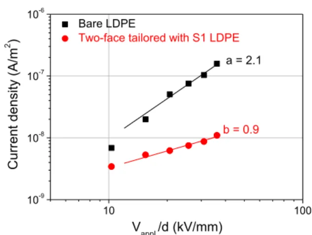
Figure 9. Current-field plot obtained for reference LDPE and LDPE with
tailored interfaces using SC electrodes. Data are relevant to charging current after 16 min of polarization.
10 100 10-9 10-8 10-7 10-6 b = 0.9 Bare LDPE
Two-face tailored with S1 LDPE
Curre nt de ns ity ( A/m 2 ) Vappl./d (kV/mm) a = 2.1 where, ε1, ε2 and γ1, γ2 are, respectively, the permittivity and
the conductivity of polymer layer 1 and 2 in sequence from the anode to the cathode. Jint is the current density at the polymer interface, which maintains continuity when the system reaches steady state, no matter the difference of effective E-field between the two polymer layers. The sign of charge density
σint can be deduced as
2 1 1 2 int 2 1 1 2 int 2 1 1 2 int 0 >0; 0 <0; 0 =0. - , - , - , (2)
The conductivity of the LDPE and the nanocomposite of 5 phr under 30 kV/mm is, respectively, γL=1.29×10⁻¹⁵ S/cm and
γN=4.43×10 -17
S/cm at room temperature. The relative permittivity of the LDPE and the nanocomposite at 0.1 Hz is
εL=2.37 and εN=2.85. In situation (-)NC/LDPE(+) in Figure 5c,
ε1=εL=2.37, ε2=εN=2.85 and γ1=γL=1.29×10⁻¹⁵ S/cm, γ2=γN=4.43×10 -17 S/cm, leading to ε2γ1-ε1γ2=3.57×10 -15 >0, so
σint>0, namely positive space charges should be accumulated at the polymer interface. With reversing the polarity of the voltage on the layers, Figure 5d, it can readily be anticipated that σint<0, namely negative space charges should be accumulated at the polymer interface. The sign of the space charge at the polymer interface calculated above is consistent with experimental results in Figures 5c and 5d. Combination of the two space charge profiles perfectly explains the space charge characteristics of the interface tailored LDPE in Figure 5b.
Therefore, it is believed that two charge dynamics happen in the nanoparticle interface tailored LDPE. On the one hand, TiO2-LDPE nanocomposite as an intercalated interface layer suppresses hole and electron injection from both electrodes due to its excellent charge suppressing ability shown in Figure 5a. The ability mainly originates from the increase of trap amount and trap level caused by TiO2 nanoparticle doping. However, this charge dynamics cannot be observed for the resolution restriction of the PEA facilities. On the other hand, the interface tailoring process introduces two dielectric/dielectric interfaces, on which heterocharges accumulate, owing mainly to a lower conductivity in the NC material than in LDPE. Definitely, the first charge dynamics has positive effects for limiting space charge accumulation whereas the second one has as consequence to increase the electric field near both electrodes and to enhance hole and electron injection, which goes against reducing charge accumulation in the LDPE substance. This should be avoided by choosing materials with proper conductivity and permittivity to reverse the sign of the interfacial charge and hence decrease the field at the electrodes.
4.1.3 PLASMA-PROCESSED NANOCOMPOSITES
Space charge measurements have shown that the AgNPs-containing nanocomposite layer acts as a very efficient barrier to injection for both electrons and holes for fields up to 50 kV/mm and considering polarity inversion. We have also shown that the effect is effective even for long time polarization. To further substantiate the results, we have plotted in Figure 9 the current-voltage characteristics obtained at room temperature for bare LDPE and for two-face tailored
LDPE. In both cases, the electrode in contact with the sample is a semiconducting material, i.e. the same configuration as for the space charge measurement results plotted in Figure 7. As can be observed, there is a substantial difference in the behavior of the two samples. First, a quantitative difference, with a drop of the apparent conductivity by about one decade in the sample with tailored interfaces, in the high field range. Second, there is a qualitative difference through a change in the slope of the current-voltage characteristic from 2 to almost 1, i.e. from what seems relevant to a space charge limited current to a behavior featuring ohmic conductivity. This appears consistent with a drastic reduction of charge injection.
4.2 PROCESS VIABILITY
We can conclude the following about the efficiency of the three modification routes:
-We confirmed that TiO2 dispersion into LDPE leads to substantial charge reduction, in line with many of literature reports using insulating inorganic particles in general and TiO2 in specific. However, at present, the association of nanocomposites of the form used and LDPE is not necessarily a reliable route as it will lead to field intensification into the LDPE layer due to charge build-up at dielectric/dielectric interface.
-Fluorination efficiently blocks negative space charge build-up but not positive one.
-AgNPs-containing nanocomposite layer efficiently prevents negative and positive charge build-up. This is the first report in the literature on this aspect.
Although charge injection control was investigated on simple laboratory structures, the work displays a panel of interface tailoring routes. Useful information is brought on process constrains, issues and merit for implementing interface modification in real systems. The process of changing the interface properties should of course be compatible with the production technology of the components. In the case of HVDC cable, surface chemical modification of the polymer could be implemented during the extrusion process, as well as incorporating NPs close to the interface. Interestingly, isolated carbon black (CB) particles near the SC
could play the role of NPs which would be compatible with available processing. The capability of isolated CB to trap efficiently both kinds of carriers is still to be demonstrated. Out of the cable application, tailoring interfacial electronic properties can be achieved by plasma deposition of thin nanostructured dielectrics. This could be particularly useful in Micro/Nano ElectroMechanical Systems (MEMS/NEMS) where insulation charging has deleterious consequences for the system operation [79].
5 CONCLUSION
Oxy-fluorination/fluorination interface tailoring markedly suppresses electron injection even under weak process conditions regardless of the introduction of oxygen atom. However, it cannot suppress hole injection and even increases net positive charge build up under strong process conditions, resulting in the increase of total space charge, presumably because the interface tailoring shallows hole traps. In addition, the introduction of O atoms hinders the fluorination reaction and enhances hole injection from anode. Interface tailoring by intercalating TiO2-LDPE nanocomposite interface layer suppresses hole and electron injection because the trap amount and trap level in amorphous region are increased by TiO2 nanoparticle doping. Furthermore, the interface tailoring process introduces two polymer interfaces, which accumulate heterocharges driven by the relative values of permittivity and conductivity in the intercalated layer and LDPE. Thin plasma deposited layers containing metallic NPs provide efficient barrier for electron and hole injection. The effect results from the trapping of charges on the particles and subsequent screening of the field at the interface with the electrode adjacent to the layer. The versatility of the plasma process makes this technique applicable to different electric components.
A
CKNOWLEDGMENTSThis work was jointly supported by Agence Nationale de la Recherche in France, project ANR-InTail under Contract No. ANR-AA-PBLI-II-2011 and China National Funds for International (regional) projects of cooperation and exchange (Grant No. 51161130524).
REFERENCES
[1] G. Chen, J. Zhao, S. Li and L. Zhong, "Origin of thickness dependent dc electrical breakdown in dielectrics," Appl. Phys. Lett., Vol. 100, p. 222904, 2012.
[2] Y. Zhang, J. Lewiner, C. Alquié and N. Hampton, "Evidence of strong correlation between space-charge buildup and breakdown in cable insulation", IEEE Trans. Dielectr. Electr. Insul, Vol. 3, pp. 778-783, 1996.
[3] L.A. Dissado, G. Mazzanti and G.C. Montanari, "The incorporation of space charge degradation in the life model for electrical insulating materials", IEEE Trans. Dielectr. Electr. Insul, Vol. 2, pp. 1147-1158, 1995.
[4] G.C. Montanari, "Bringing an insulation to failure: the role of space charge", IEEE Trans. Dielectr. Electr. Insul., Vol. 18, pp. 339-364, 2011.
[5] C. Laurent, G. Teyssèdre, S. Le Roy and F. Baudoin, "Charge dynamics and its energetic features in polymeric materials", IEEE Trans. Dielectr. Electr. Insul., Vol. 20, pp. 357-381, 2013. [6] T. Hjertberg, V. Englund, P.O. Hagstrand, W. Loyens, U.
Nilsson and A. Smedberg, "Materials for HVDC cables", Revue Electricité Electronique, No. 4, pp. XI-XV, 2014.
[7] S. Hole and J. Lewiner, "High-resolution multidimensional space charge measurement using elastic wave methods", Phys. Rev. B, Vol. 64, p. 104106, 2001.
[8] R.J. Fleming, "Space charge profile measurement techniques: recent advances and future directions", IEEE Trans. Dielectr. Electr. Insul., Vol. 12, pp. 967-978, 2005.
[9] M. Fukuma, G. Teyssedre, C. Laurent and K. Fukunaga, "Millisecond-time range analysis of space charge distribution and electroluminescence in insulating polymers under transient electric stress", J. Appl. Phys., Vol. 98, p. 093528, 2005. [10] M. Meunier, N. Quirke and A. Aslanides, "Molecular modeling
of electron traps in polymer insulators: chemical defects and impurities", J. Chem. Phys., Vol. 115, pp. 2876-2881, 2001. [11] A. Huzayyin, S. Boggs and R. Ramprasad, "Quantum
mechanical studies of carbonyl impurities in dielectric polyethylene", IEEE Trans. Dielectr. Electr. Insul., Vol. 17, pp. 926-930, 2010.
[12] G. Teyssedre, C. Laurent, G. Perrego and G.C. Montanari, "Charge recombination induced luminescence of chemically modified cross-linked polyethylene materials", IEEE Trans. Dielectr. Electr. Insul., vol. 16, pp. 232-240, 2009.
[13] Y. Murakami, M. Nemoto, S. Okuzumi, S. Masuda, M. Nagao, N. Hozumi, Y. Sekiguchi and Y. Murata, "DC conduction and electrical breakdown of MgO/LDPE nanocomposite", IEEE Trans. Dielectr. Electr. Insul., vol. 15, pp. 33-39, 2008. [14] J.K. Nelson, "Nanodielectrics – the first decade and beyond",
Proc. Int'l Symp. Electr. Insul. Mat. (ISEIM, Niigata City, Japan), pp. 1-11, 2014.
[15] I. Plesa, P.V. Notingher, S. Schlögl, C. Sumereder and M. Muhr, "Properties of polymer composites used in high-voltage applications", Polymers, vol. 8, p. 173 (pp. 1-63), 2016. [16] N.M. Burns, "Performance of supersmooth, extra-clean
semiconductive shields in XLPE insulated power cables", Proc. IEEE Int'l. Sympos. Electr. Insul. (ISEI, Toronto, Canada), pp. 272-276, 1990.
[17] G. Chen, Y. Tanaka, T. Takada and L. Zhong, "Effect of polyethylene interface on space charge formation," IEEE Trans. Dielectr. Electr. Insul., Vol. 11, pp. 113-121, 2004.
[18] M. Taleb, G. Teyssèdre and S. Le Roy, "Role of the Interface on Charge Build-up in a Low-Density Polyethylene: Surface Roughness and Nature of the Electrode", IEEE Conf. Electr. Insul. Dielectr. Phenom. (CEIDP), pp. 112-115, 2009.
[19] M. Jeroense, M. Saltzer and H. Ghorbani, "Technical challenges linked to HVDC cable development", Revue Electricité Electronique, No. 4, pp. III-X, 2014.
[20] U.H. Nilsson, J. Andersson, V. Englund, V. Eriksson, P.O. Hagstrand and A. Smedberg, "The role and measurement of dc conductivity for HVDC cable insulation materials", IEEE Conf. Electr. Insul. Dielectr. Phenom. (CEIDP), pp. 31-34, 2015. [21] Z. An, Q. Yang, C. Xie, Y. Jiang, F. Zheng and Y. Zhang,
"Suppression effect of surface fluorination on charge injection into linear low density polyethylene" J. Appl. Phys., Vol. 105, p. 064102, 2009.
[22] Y. Jiang, Z. An, C. Liu, F. Zheng and Y. Zhang, "Influence of oxyfluorination time on space charge behavior in polyethylene", IEEE Trans. Dielectr. Electr. Insul., Vol. 17, pp. 1814-1823, 2010.
[23] K. Takashima and T. Oda, "Space and Surface Charge Behavior Analysis of Plasma Pre-processed Dielectric Thin Films", IEEE Trans. Indust. Appl., vol. 35, pp. 1192-1197, 1999.