HAL Id: hal-02263545
https://hal-amu.archives-ouvertes.fr/hal-02263545
Submitted on 10 Nov 2020
HAL is a multi-disciplinary open access
archive for the deposit and dissemination of sci-entific research documents, whether they are pub-lished or not. The documents may come from teaching and research institutions in France or abroad, or from public or private research centers.
L’archive ouverte pluridisciplinaire HAL, est destinée au dépôt et à la diffusion de documents scientifiques de niveau recherche, publiés ou non, émanant des établissements d’enseignement et de recherche français ou étrangers, des laboratoires publics ou privés.
Binary Compound Semiconductors
Jean-Luc Autran, Daniela Munteanu
To cite this version:
Jean-Luc Autran, Daniela Munteanu. Atmospheric Neutron Radiation Response of III-V Binary Compound Semiconductors. European Workshop on Radiation and its Effects on Components and Systems (RADECS 2019), Sep 2019, Biarritz, France. �hal-02263545�
Abstract—This works examines the radiation response of III-V binary compound semiconductors subjected to high energy atmospheric neutrons. Production of neutron-induced secondary products and implications for single event effects are carefully analyzed and discussed.
Index Terms—atmospheric neutrons, binary compound semiconductors, III-V materials, neutron cross section, elastic scattering, noneleastic interactions, nuclear data library, Geant4, numerical simulation.
I. INTRODUCTION
Beyond optoelectronics, high-frequency or integrated power applications, III-V semiconductor materials are becoming attractive materials for advanced CMOS nanoelectronics; they are currently extensively investigated in the perspective of silicon replacement for both n-channel and p-channel materials in CMOS, due to higher carrier mobilities for both electrons (GaAs, InAs, InGaAs, InP) and holes (GaSb, InGaSb) with respect to Si and compatibility with high-k dielectric-based gate stacks [1-3]. A recent work demonstrated that nanowire n-type (InAs) and p-type (GaSb) transistors can be co-processed and co-integrated in a viable alternative to current CMOS silicon technology, offering increased drive-currents up to 1800 µA/µm for the n-MOS device [4].
From a radiation effect point-of-view, total ionizing dose (TID), heavy ion and laser responses of III-V MOS transistors in modern architectures have been recently studied [5-7]. III-V materials and related devices have been also extensively investigated from the perspective of the creation mechanisms of single event effects [8-10] but relatively little work concerns their response to atmospheric neutrons. The aim of this work is precisely to examine the radiation response of III-V binary compound semiconductors subjected to high energy atmospheric neutrons. The paper is organized as follows. Section II presents the different compound materials studied and summarizes their main properties. Section III details the direct and Geant4 calculation of the atmospheric neutron reaction rate in a layer of material; section IV presents a complete analysis of neutron-induced secondaries produced in these III-V materials using Geant4. Finally, implications for single event effects are discussed in the conclusion of this work.
J.L. Autran and D. Munteanu are with Aix-Marseille Univ, CNRS, Université de Toulon, IM2NP, UMR 7334, Faculté des Sciences, F-13397 Marseille Cedex 20, France (e-mail: [email protected]).
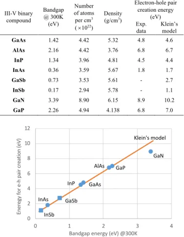
TABLE I.MAIN PROPERTIES OF THE III-V BINARY COMPOUNDS STUDIED IN THIS WORK. III-V binary compound Bandgap @ 300K (eV) Number of atoms per cm3 ( ´1022) Density (g/cm3) Electron-hole pair creation energy (eV) Exp. data Klein’s model GaAs 1.42 4.42 5.32 4.8 4.6 AlAs 2.16 4.42 3.76 6.8 6.7 InP 1.34 3.96 4.81 4.5 4.4 InAs 0.36 3.59 5.67 1.8 1.7 GaSb 0.73 3.53 5.61 - 2.7 InSb 0.17 2.94 5.78 - 1.1 GaN 3.39 8.90 6.15 8.9 10.2 GaP 2.26 4.94 4.138 6.8 7.0
Fig. 1. Energy for e-h pair creation as a function of the bandgap energy for the III-V binary compound materials studied in this work.
II. MATERIAL PROPERTIES AND NUCLEAR DATA LIBRARIES
In this work, the atmospheric neutron response of eight III-V binary compound materials have been studied: GaAs, AlAs, InP, InAs, GaSb, InSb, GaN and GaP (GaAs and GaN materials have been recently explored in [11]). Table I summarizes the main experimental values for these materials in terms of bandgap, density, and electron-hole pair creation energy. This last data is missing in literature for GaSb and InSb; we used values deduced from the Klein’s model [12] linking energy bandgap and energy for e-h pair creation in semiconductor materials (Fig. 1). 0 2 4 6 8 10 12 0 1 2 3 4 En er egy fo r e -h pa ir cr ea tion (e V)
Bandgap energy (eV) @300K
GaN GaP AlAs GaAs InP GaSb InAs InSb Klein's model
Atmospheric Neutron Radiation Response
of III-V Binary Compound Semiconductors
TABLE II. NATURAL ABUNDANCE OF NUCLIDES RELATED TO III-V BINARY COMPOUNDS MATERIALS STUDIED IN THIS WORK AND AVAILABILITY OF CROSS SECTION IN EDNFB-VII.1 AND TENDL-2017 NUCLEAR DATA LIBRARIES.
Symbol number Atomic Nuclide abundance Natural
ENDFB-VII.1. (20 MeV) TENDL-2017 (200 MeV) Al 13 13-Al-27 100.00% ✓* ✓ Ga 31 31-Ga-69 60.10% ✓ ✓ 31-Ga-71 39.90% ✓ ✓ In 49 49-In-115 95.70% ✓ ✓ 49-In-113 4.30% ✓ ✓ N 7 7-N-14 99.60% ✓ * ✓ 7-N-15 0.40% ✓ ✓ P 15 15-P-31 100.00% ✓* ✓ As 33 33-As-75 100.00% ✓ ✓ Sb 51 51-Sb-121 57.40% ✓ ✓ 51-Sb-123 42.60% ✓ ✓ Si 14 14-Si-28 92.20% ✓* ✓ 14-Si-29 4.70% ✓* ✓ 14-Si-30 3.10% ✓* ✓ *Extended to 120 MeV
Fig. 2. High energy (> 1 MeV) neutron cross sections for the main nuclides related to the III-V materials studied. Data from the TENDL-2017 nuclear data library.
The III-V binary compounds studied in the following are made from seven chemical elements from columns III (Al, Ga, In) and V (N, P, As, Sb) of the periodic table. We voluntary excluded boron-based compounds (BN, BP, BAs, BSb) from this study, due to the thermal neutron sensitivity of these materials (if not selective in isotopes) induced by the presence
of 10B. Table II indicates the isotope composition of these
elements and their natural abundance. The study of atmospheric neutron interactions with the compounds of Table I requires: i) the availability of neutron cross-sections for all nuclides listed in Table II and ii) if possible, an extended energy range above 1 MeV, due to the nature of the atmospheric neutron spectrum [13]. Even if the US standard evaluated nuclear data library ENDF/B (ENDFB-VII.1) [14] responds well to the first point (in particular for In and Sb that are not included in all nuclear
data libraries), however, the upper energy limit is only 20 MeV for Ga, In, Sb and As. After checking of several nuclear data libraries, we choose the new release of the TENDL library (TENDL-2017) [15] that offers availability of all neutron cross-sections up to 200 MeV. Fig. 2 shows the total cross cross-sections for the most abundant nuclides for the seven elements and also for 14-Si-28 for comparison. These data are used in the next section to evaluate the neutron reaction rate in a layer of the different compound materials.
III. NEUTRON REACTION RATES IN A LAYER OF MATERIAL
The susceptibility of the studied materials to atmospheric neutron has been roughly evaluated by a direct calculation of the reaction rate in a target representative of a microelectronic circuit, following a method introduced by Wrobel et al [16].
According to [16], we first calculated the number of nuclear
reactions Rn in a material layer with an area of S=1 mm2, a
thickness of e=1 µm and an atomic density equal to that of
silicon (N=5 ´1022 at./cm3). Rn is simply given by:
𝑅"= 𝑁𝑒 ∫-.1"-./0𝜎(𝐸)+,+-𝑑𝐸 (1)
where s(E) is the neutron cross section of the considered
element constituting the material, dj/dE is the differential neutron flux (measured by Goldhagen and modeled by Gordon
et al. [13]), Emin and Emax are the limits of the energy domain
considered (in the following, Emin = 1 MeV and Emax = 200
MeV).
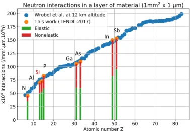
Fig. 3 shows the results of our calculations using Eq. (1) applied to “materials” constituted by a single element of Table II with an isotope composition mimicking the natural abundance. In order to compare with Wrobel’s data, nuclear
rates are expressed for a duration of 109 h and for a neutron flux
corresponding to 12 km altitude. Our results shown in Fig. 3 are in very good agreement with Wrobel’s data. For each element, we give in addition the number of elastic and nonelastic events directly evaluated from TENDL-2017 (MF=3, MT=2 for elastic cross section).
Fig. 3. Calculated number of nuclear interactions in 109 h induced by high
energy (>1 MeV) atmospheric neutrons in la layer of material of 1 mm2. Data
are compared to previous results published in [16].
N AlSi
P Ga
As
Fig. 4. Calculated number of nuclear interactions induced by atmospheric neutrons in different III-V binary compound materials (exact composition with natural abundance of nuclides) deduced from Eq. (1) for ENDFB-VII.1 and TENDL-2017 nuclear data libraries and from Monte Carlo simulations using Geant4.
From data of Fig. 3, the reaction rates for all the III-V materials of Table I can be deduced, taken into account the
exact number of atoms per cm3 and the binary nature of the
compounds. In order to compare with our previously published results on Si [17], Ge and SiC [11], we change in the following the normalization factors introduced for the expression of the
nuclear rates, choosing now: S = 1 cm2, e = 20 µm, duration of
5x10⁶ h and neutron flux at sea level. With respect to Wrobel’s
conditions previously used in Fig. 3, these differences result in new reaction rates equal to Wrobel’s ones exactly divided by a numerical factor of 50.
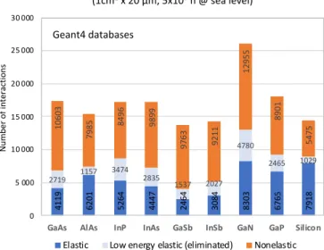
Fig. 4 shows the results of these calculations for nuclear interaction rates evaluated from ENDFB-VII.1 and TENDL-2017 nuclear data libraries and from Monte Carlo simulations using Geant4 (8 separate runs for each compound as the target material). Details for Geant4 simulations can be found in Ref. [11]. With respect to Fig. 3, the neutron reaction rates considering the exact number of atoms per volume unit leads to significantly narrow the range of values: almost all materials, GaN excepted, exhibit similar global reaction rates, between 13,000 and 18,000 for Geant4 simulations. Between all materials, GaSb and InSb show the number of interaction events the closest from the one of Si. Geant4 values are logically found greater to those derived from ENDFB-VII.1 (limited to 20 MeV in energy) but slightly lower to those obtained with TENDL-2017 (statistically considering, in this case, more events at high energies). In the next section, Geant4 databases are analyzed in order to examine in detail the production of secondaries for the different binary compounds.
IV. DETAILED ANALYSIS OF SECONDARY PRODUCTS
For standardization purposes [11,17], we eliminated in the following all secondary particles not able to deposit an electrical charge in the target material above a certain threshold quantity, fixed in previous studies equal to 1.8 fC [17]. This database post-treatment eliminates from the following analysis
the less energetic recoils and all g photons, p0, rare p+ and p-,
e+, e- and h particles, not able to induce a single event transient
susceptible to lead to an error in a given circuit. This
Fig. 5. Number of elastic and nonelastic interactions induced by atmospheric neutrons in the different III-V binary compound materials obtained from Geant4 simulations. The number of low energy elastic events eliminated from the different databases are also indicated.
Fig. 6. Distribution of products resulting from the interactions of atmospheric neutrons with the different III-V binary compound materials obtained from Geant4 simulations. The low energy elastic events eliminated from the different databases are also indicated.
mechanically decreases the number of elastic events (less energetic events).
Fig. 5 shows the distributions of elastic and nonelastic events for the different III-V compound materials. The number of low energy elastic events, eliminated from the different databases following the threshold criterion previously defined, are also indicated. Contrary to silicon (shown for comparison) which is known to produce 40% of nonelastic events under atmospheric neutrons, all materials exhibit more nonelastic than elastic events. This proportion of nonelastic events ranges from 56% for AlAs up to 80% for GaSb. GaN show the highest number of
0 5000 10000 15000 20000 25000 30000
GaAs AlAs InP InAs GaSb InSb GaN GaP Silicon
N umb er o f i nte racti on s
Atmospheric neutron interactions (1cm2x 20 µm, 5x10⁶h @ sea level)
ENDFB-VII.1 Geant4 TENDL-2017
4119 6201 5264 4447 2464 3084 8303 6765 7918 2719 1157 3474 2835 1537 2027 4780 2465 1029 10603 7985 8496 9899 9763 9211 12955 8901 5475 0 5 000 10 000 15 000 20 000 25 000 30 000
GaAs AlAs InP InAs GaSb InSb GaN GaP Silicon
N umb er o f i nte racti on s
Atmospheric neutron interactions (1cm2x 20 µm, 5x10⁶h @ sea level)
Elastic Low energy elastic (eliminated) Nonelastic
Geant4 databases 0 5000 10000 15000 20000 25000 30000 35000
GaAs AlAs InP InAs GaSb InSb GaN GaP Si
Nu m be r o f p ro du ct s
Secondaries produced in all interactions (1cm2x 20 µm, 5x10⁶h @ sea level)
protons alphas Recoils #1 Recoils #2 Others
Ga As Al As P In In In Sb Sb As Ga Ga N P Ga Si
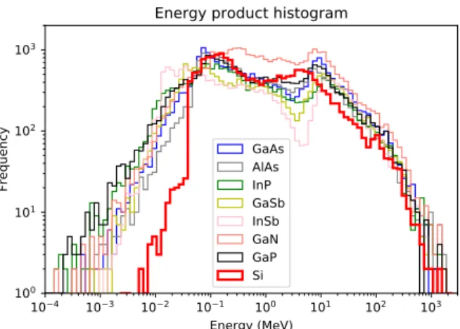
Fig. 7. Energy histograms of all secondary products induced by atmospheric neutron interactions in the different III-V material targets (also including silicon for comparison).
Fig. 8. Total number of e-h pairs induced by all secondaries in the different III-V material targets normalized with respect to the value obtained for silicon.
interactions in both categories, elastic and nonelastic, mainly due to the number of atoms per volume unit for this compound semiconductor which is almost double with respect to all other materials (see Table I).
Fig. 6 shows the distribution of all secondaries produced by atmospheric neutron interactions in the different targets of III-V binary compound materials; Fig. 7 gives their energy distribution. Four groups of particles have been defined in Fig. 6: protons, alpha particles, nuclei corresponding to target atoms (named recoils #1 and #2 indexed as a function of increasing Z) and other nuclei. Similar distributions of these particle groups are found for all materials, GaN excepted, with approximately 25% of protons+alphas, 60% of target nuclei and the remaining 15% of other nuclei. For GaN, a higher proportion of protons and alpha particles is observed (40%), due to significant cross
sections for 14N(n,p)14C and 14N(n,a)11B reactions. Additional
results and histograms per product category will be analyzed in the final paper, notably in terms of particle LET, range, angular distribution, shower multiplicities and reaction channels.
V. IMPLICATIONS FOR THE SEES
Concerning SEEs, one interesting global metric is the amount of electrical charge indirectly deposited by atmospheric neutrons in the different material targets. Fig. 8 shows this total number of e-h pairs induced by all secondaries for the different III-V compounds with respect to the value obtained for silicon.
Three groups of materials can be distinguished in Fig. 8: GaAs, AlAs, InP, GaN and GaP that are finally found very similar to Si in terms of e-h pair generation (relative factor close to 1), InAs and GaSb which exhibit a factor between 1.5 and 2.5 and, finally, InSb characterized by the highest factor, close to 4. This result suggests a susceptibility to atmospheric neutrons at material level more important for InSb, InAs and GaSb than the one observed in the other compounds and in silicon.
This preliminary exploration of III-V binary compound materials should be now completed by the evaluation of the impact of carrier mobilities and lifetimes on the formation of single-event transients in reversely biased junctions to conclude on their level of vulnerability to natural neutron radiation at ground level.
VI. REFERENCES
[1] H. Riel, L. Wernersson, M. Hong, J. Del Alamo, “III–V compound semiconductor transistors—from planar to nanowire structures”, MRS Bulletin, 39(8), 668-677, 2014.
[2] S. Oktyabrsky, P. Ye, Fundamentals of III-V Semiconductor MOSFETs, Springer Science & Business Media, 2010.
[3] T. Li, M. Mastro, A. Dadgar, III–V Compound Semiconductors: Integration with Silicon-Based Microelectronics, CRC Press, 2016. [4] A.A. Jönsson, J. Svensson and L. Wernersson, “A Self-Aligned Gate-Last Process Applied to All-III–V CMOS on Si,” IEEE Electron Device Letters, vol. 39, no. 7, pp. 935-938, July 2018. [5] K. Ni et al., “Single-Event Transient Response of InGaAs
MOSFETs,” in IEEE Transactions on Nuclear Science, vol. 61, no. 6, pp. 3550-3556, Dec. 2014.
[6] H. Gong et al., “Scaling Effects on Single-Event Transients in InGaAs FinFETs,” in IEEE Transactions on Nuclear Science, vol. 65, no. 1, pp. 296-303, Jan. 2018.
[7] H. Gong et al., “Pulsed-Laser Induced Single-Event Transients in InGaAs FinFETs on Bulk Silicon Substrates,” IEEE Transactions on Nuclear Science, vol. 66, no. 1, pp. 376-383, Jan. 2019. [8] C.H. Tsao, R. Silberberg and J.R. Letaw, “A comparison of
neutron-induced SEU rates in Si and GaAs devices,” IEEE Transactions on Nuclear Science, vol. 35, no. 6, pp. 1634-1637, Dec. 1988. [9] T.T. Vu, Compound Semiconductor Integrated Circuits, World
Scientific, 2003.
[10] D. McMorrow, J.S. Melinger, A.R. Knudson, “Single-event effects in III-V semiconductor electronics”, International Journal of High-Speed Electronics and Systems Vol. 14, No. 2, 311-325, 2004. [11] D. Munteanu D and J.L. Autran, “Susceptibility of Group-IV and
III-V Semiconductor-based Electronics to Atmospheric Neutrons Explored by Geant4 Numerical Simulations”. In: S. Rao (Ed.) Numerical Simulations, Intech, Vienna, pp. 117-134, 2018. [12] C.A. Klein, “Bandgap Dependence and Related Features of
Radiation Ionization Energies in Semiconductors”, Journal of Applied Physics. 39. 2029 – 2038, 1968.
[13] M.S. Gordon et al., “Measurement of the Flux and Energy Spectrum of Cosmic-Ray Induced Neutrons on the Ground,” IEEE Transactions on Nuclear Science, vol. 51, pp. 3427-3434, 2004. [14] M.B. Chadwick et al. “ENDF/B-VII.1 Nuclear Data for Science and
Technology: Cross Sections, Covariances, Fission Product Yields and Decay Data,” Nuclear Data Sheets, vol. 112, pp. 2887-2996, 2011.
[15] D. Rochman, A.J. Koning, J.Ch. Sublet, M. Fleming, et al., "The TENDL library: hope, reality and future", proceedings of the International Conference on Nuclear Data for Science and Technology, September 11-16, 2016, Bruges, Belgium.
[16] F. Wrobel, J. Gasiot, F. Saigné, and A.D. Touboul, “Effects of atmospheric neutrons and natural contamination on advanced microelectronic memories”, Appl. Phys. Lett. 93, 064105, 2008. [17] S. Serre, S. Semikh, S. Uznanski, J.L. Autran, D. Munteanu, G.
Gasiot, P. Roche, “Geant4 Analysis of n-Si Nuclear Reactions From Different Sources of Neutrons and Its Implication on Soft-Error Rate”, IEEE Transactions on Nuclear Science, Vol. 59, no. 4, pp. 714-722, 2012. 1.15 0.68 1.03 2.49 1.69 3.92 0.89 1.07 1.00 0 0.5 1 1.5 2 2.5 3 3.5 4 4.5
GaAs AlAs InP InAs GaSb InSb GaN GaP Si
Re
lati
ve
facto
r