OATAO is an open access repository that collects the work of Toulouse
researchers and makes it freely available over the web where possible
Any correspondence concerning this service should be sent
to the repository administrator:
[email protected]
This is an author’s version published in:
http://oatao.univ-toulouse.fr/20820
To cite this version:
Taghia, Bouazza and Billard, Thibaut and Carayon,
Jean-Pierre and Malec, David and Piquet, Hubert and Belinger,
Antoine Investigations on Partial Discharges risk in
aeronautical rotating machine fed by HVDC 540Vdc network.
(2018) In: 2018 IEEE Electrical Insulation Conference (EIC),
17-20 June 2018 (San Antonio, United States)
Official URL:
https://doi.org/10.1109/EIC.2018.8481115
Investigations on Partial Discharges risk in aeronautical
rotating machine fed by HVDC 540Vdc network
Bouazza TAGHIA, Thibaut BILLARD, Jean-Pierre CARAYON
IRT Saint Exupéry Toulouse, France
[email protected] [email protected] [email protected]
David MALEC, Hubert PIQUET, Antoine BELINGER
LAPLACE, Université de Toulouse, CNRS Toulouse, France
[email protected] [email protected] [email protected]
Abstract— The voltage level aboard new aircraft generations
has grown from 115VAC to 230VAC. This has given rise to a new HVDC +/- 270V instead of +270V. The Adjustable Speed Drives (ASD) aboard more electrical aircraft are currently fed by fast switching PWM IGBT converters which rise time and fall time are higher than 50ns. To improve the converters power density, the very fast Wide Bandgap semiconductor technologies (Silicon Carbide) are currently under evaluation; their switching rise time and fall time could be lower than 20ns. This paper, by using industrial ASD fed by 540Vdc, initially addresses an experimental investigations analysis of motor overvoltages according to: inverters technologies (IGBT and SiC), harness length and harness shielding. Then, investigations on the Partial Discharges Inception Voltage (PDIV) are carried out on primary components of Electrical Insulation System (EIS) type 1 at atmospheric and reduced pressures, according to several parameters: magnet wire (MW) diameter, MW grade, polyimide insulating paper thickness. The paper concludes with a discussion of the different results and thoughts about overvoltages and partial discharges challenges.
Keywords – Partial Discharges (PD), Overvoltage, Adjustable Speed Drives (ASD), More Electrical Aircraft (MEA).
I. INTRODUCTION
The use of IGBT in ASD ensures speed control with very good energy efficiency. Inverters based on SiC components allow even better performances. Reduced losses allow higher switching frequency than with IGBT, therefore offer a better controllability for high speed motors.
In this paper we analyze the impact of this new technology on transient overvoltages phenomena. These latter are able to deteriorate the ASD reliability by creating partial discharges (PD). The motor is the most vulnerable element in terms of PD risks, so in this paper we focus on overvoltages at its terminals and PDIV of its EIS.
II. OVERVOLTAGE IN AERONAUTICAL ADJUSTABLE SPEED DRIVE: EXPERIMENTAL INVESTIGATIONS
A. Test bench description
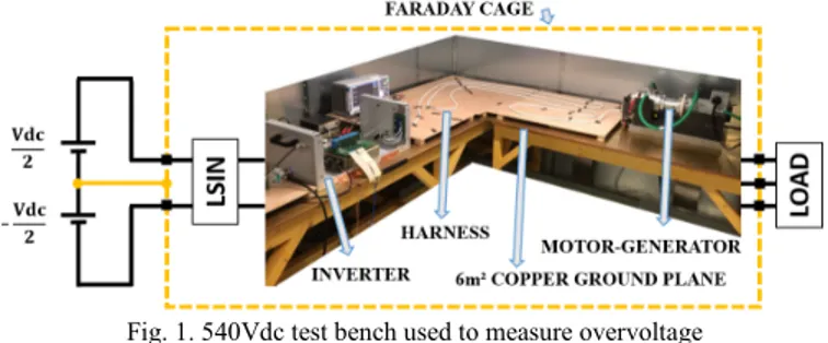
To perform experimental investigations on overvoltage phenomena, we use a 15kW three-phase ASD developed according to the aeronautic standard DO-160 (Fig. 1); it is composed mainly of : (1) DC +/- 270V power supply, which simulates the HVDC aircraft network. (2) LISN: the line impedance stabilization network ensures the return of the
common mode currents caused by the inverter switching and prevents the supply harmonics to enter in the ASD. (3) Inverter: It is a two-level converter, which provides DC/AC conversion. Two inverter technologies are used: Si-IGBT-20 kHz and SiC-MOSFET-30kHz. In this paper we use a natural PWM (sinus-triangle) for switching control. (4) Harness: Provides the power transmission between inverter and motor: three shielded and unshielded harness configurations are tested: DM-AWG8-2m, DR-AWG10-10m and DR-AWG10-20m. (5) Motor: It is a high speed aeronautical permanent magnet synchronous motor coupled to a generator machine. This one is connected to configurable test bench load.
The ASD is placed on a 6m² copper ground plane, the whole system is installed in a Faraday cage. The connections between the inside and outside of the cage passes through a filters. Note that the ASD doesn’t include dv/dt filters or EMI filters.
The voltages are measured using an oscilloscope and voltage probes with a bandwidth greater than 300 MHz.
Fig. 1. 540Vdc test bench used to measure overvoltage
B. Three phases inverter output voltage behavior: SiC-MOSFET technology vs. Si-IGBT technology
Among the advantages of using SiC-MOS components in power electronic converters is reduction of the energy losses. Converter with lower losses implies better efficiency, lower weight by reducing need of cooling. For aeronautical application, low weight is a crucial requirement. However, this technology could have a harmful impact on EMI issues in general, and on overvoltages across electrical insulation system in particular.
To evaluate the impact of SiC-MOS technology on motor overvoltage, we refer to an inverter with a Si-IGBT technology. The idea here is to measure the switching durations. Hence, for both technologies, we have measured: (1) the voltage across the bottom component of the inverter leg a (Ua-). (2) The current coming out of the same inverter leg (Ia).
fall time (tf) between 10% and 90% according to the IEEE
definition.
Fig. 2 and Fig. 3 show an example of a result for the operating point: (Vdc = 540V, Iinverter = 36Arms, ffond = 330Hz). We
emphasize that the switching time tr and tf are strongly
dependent on the switched instantaneous current.
Si-IGBT behavior: For Ia>0, tr is minimal and equal on average
to 50ns, while tf varies between 1500ns and 150ns depending
on Ia value. For Ia<0, tf has the same behavior of tr during Ia>0.
The tr has also the same behavior of tf during Ia>0 but with
average value of 70ns. This asymmetry causes negative overvoltage values higher than positive ones.
SiC-MOS behavior: For Ia>0, tr is minimal and equal on
average to 15ns, while tf varies between 1000ns and 50ns
depending on Ia value. For Ia<0, tr has the same behavior of tf
during Ia>0 and tf has the same behavior of tr during Ia>0. The
irregular peaks contained in the tr and tf curves are due to the
post-processing script.
In terms of speed performances, the SiC-MOS inverter is 3 times faster than the Si-IGBT inverter. In general term, tr and tf
trends generated by SiC-MOS are similar to those of Si-IGBT, except for low current values. As can be seen in Fig. 2 Si-IGBT switches slowly when the current passes through zero: tr
and tf are high at same time. In other words, at no-load or low
current operations, the IGBT switches slowly comparing to the rated operating conditions. While for SiC-MOS (Fig. 2), there is no time interval during which tr and tf are both high.
Fig. 2. Rise time tr and fall time tf of Si-IGBT inverter
Fig. 3. Rise time tr and fall time tf of SiC-MOS inverter
C. Overvoltage at motor terminals
We can distinguish two electrical constraints at motor terminals:
1) Phase to phase voltage (also called differential
mode voltage Vdm): As shown by measurements of Fig. 4, after
the inverter switching, the motor Vdm passes by a damped
sinusoidal transient regime before stabilizing around the DC voltage in steady state (Vdc = 540V in our case). These phenomena have been extensively studied for ASD based on IGBT converters. Their maximal value depends mainly on the inverter speed (tr and tf) and the harness propagation delay tp.
By using the transmission line theory[1][2], it is shown that Vdm overvoltage reaches its maximum value (2*Vdc) when (tr
or tf) <tp/2. Their resonance frequency varies from few MHz
to few 10 MHz; it is imposed mainly by the harness and equal to 1/(4*tp). Phase to phase voltage stresses the insulation between phases and potentially the inter-turns insulation by voltage propagation effect along winding[3].
2) Phase to ground voltage (also called common mode
voltage Vcm): In our experimental manipulation, all the
grounds of ASD equipments are connected to the copper ground plane (representing the aircraft structure), this latter is connected to the mid-point of the power supply (Fig. 1). This implies that the voltage Vcm is a bipolar voltage varying
between -VDC/2 and VDC/2. As shows by measurements of Fig. 4, after inverter switching, the motor phase to phase
voltage passes by a transient regime before stabilizing around -270V or 270V. The Vcm transient behavior is a result of
complex interaction between the differential mode electrical components (mainly: inductances and resistances) with all the ASD common mode capacitances. Unlike the Vdm, very few
studies have been dedicated to rigorous study of Vcm. Phases
to ground voltage stresses the ground insulation and contributes to the creation of the shaft voltage[4].
Fig. 4. Example of measured Vdm and Vcm motor voltage for Vdc=540V,
Iinverter=36Arms, Harness length=20m.
In what follows we present a parametric study of these two voltages Vdm and Vcm: according to the inverter technology
and to six different harness configurations.
D. Measured overvoltage at motor terminals: influence of inverter technology and harness length
The transmission line behavior of the harness plays a primary role in creating overvoltage. The harness length influences quasi-linearly the propagation time tp. This value determines the harness critical length Lc (corresponding to
tp=2*(tr or tf)). The harness can be shielded or unshielded. The
shield ensures the return of common mode noise currents, then the area of loops causing the radiation are smaller. Its effect on overvoltages is presented below.
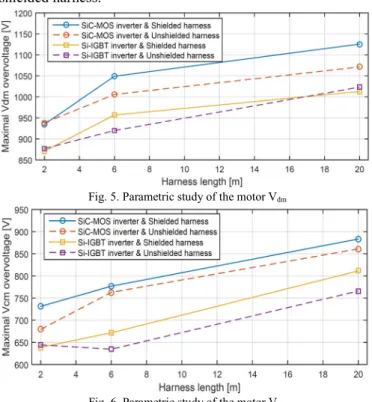
Twenty-four experimental setups were tested, using six harness configurations: DM-AWG8-2m, DR-AWG10-10m and DR-AWG10-20m cables, shielded and unshielded. The results are represented in Fig. 5 and Fig. 6; only the maximum overvoltages over two electrical periods are retained. The following points can be observed:
Harness length: Increasing the harness length from 2m to 20m
can involve increasing of Vdm and Vcm up to 180V.
Shielded harness vs. unshielded harness: Harness shielding can
provide an increase of Vdm and Vcm up to 50V.
SiC-MOS vs. Si-IGBT: Compared to a Si-IGBT inverter, the
use of a three times faster SiC-MOS inverter involves: (1) the Vdm increasing from 70V to 100V and (2) the Vcm increasing
of Vcm of 100V on average.
More generally, for a given length, a variation up to 150V of the overvoltages (Vdm and Vcm) at the terminals of the motor
can be observed, according to the following parameters: shielding or not and inverter technology (Si-IGBT-20kHz-50ns and SiC-MOS-30kHz-15ns). In terms of maximal overvoltage values, for the presented operating point, Vdm is
about 1125V and Vcm about 880V. They are obtained by using
an ASD with SiC-MOS inverter and DR-AWG10-20m shielded harness.
Fig. 5. Parametric study of the motor Vdm
Fig. 6. Parametric study of the motor Vcm
III. PARTIAL DISCHARGE ELECTRICAL INSULATION SYSTEM TYPE1
Currently, most aeronautical motors use a low voltage Electrical Insulation System (EIS) type 1 (<1000V). The EIS is
composed mainly of: (1) the enameled wire (generally with round form), which is also called Magnet Wire (MW), (2) the ground insulating papers and (3) phase to phase insulation. The EIS type 1 is based on polymers that are not intended to operate under partial discharges (PD) phenomena. The PD occur in the EIS when the voltage level across the insulation exceeds the partial discharge inception voltage (PDIV). The EIS type 1 lifetime under DP phenomena can be dramatically reduced from 20000 hours to a few hours, or even few minutes, depending on the difference between the voltage across the EIS and its PDIV.
The idea here is to investigate the PDIV values of the most commonly used EIS primary components. We are limited in this paper only to the worst case configurations. Indeed, the effect of the varnish on the increase of the PDIV is not presented.
A. Partial Discharges: Experimental setup
To evaluate worst cases of the turn to turn PDIV and the phase to phase PDIV, we realize measurements on twisted pair samples formed according to the recommendation of the IEC 60851-5 standard. The twisted pair PDIV can represent: (1) Stress between two turns in contact (case usually faced on random wound motors supplied by steep front voltage) (2) two phases in contact due to absence of end winding insulating paper.
It is usual to use a ‘motorette’ for ground insulation testing. Unfortunately, the parameters of this solution are not fixed by a standard. As part of our objectives presented above, in order to get PDIV with repeatable and reproducible measurements, we suggest to use the simple setup shown in Fig. 7.b: it consists of a superposition of a magnet wire, insulating paper and a ground plane; this assembly is held in contact with a small force applied by a mechanical spring.
To measure PDIV, we used the experimental test bench detailed in [5]. In case of twisted pairs, a 50Hz sinusoidal voltage is applied to one magnet wire and the other is grounded. In the case of the ground insulation test, the 50Hz sinusoidal voltage is applied to the magnet wire and the metal plane is grounded (Fig. 7). The voltage is gradually increased until the PDIV. To take into account the dispersion due to the measurement operating procedure and the materials dispersion, we measure the PDIV on 100 tests (10 samples and 10 tests on each sample); then a statistical interval is calculated with a 95% confidence coefficient.
B. MW PDIV vs. MW diameter and MW insulation thickness
The MW is studied according to its two characteristic parameters: diameter and grade. The latter represents the thickness of the enamel according to the IEC 60317-13 standard. The grade corresponds on average to the following radial thicknesses: grade1=43μm, grade2=60μm and grade3=80μm. Three MW diameters are tested: 0.5mm, 0.71mm and 1mm. The results are shown in Fig. 8.
Fig. 8. PDIV of MW vs. wire diameter and enamel thickness For the tested geometric intervals, doubling the MW diameter or its enamel thickness increases the PDIV about 30%. Indeed, a larger diameter allows more smooth contact curvature, therefore, lower electric fields. A higher enamel thickness reduces the electric field values too. Reducing the electric field intensity in the air gap surrounding MW reduces the PDIV.
C. Phase to ground insulation
Fig. 9 below presents the positive contribution of the polyimide paper thickness on the PDIV. The MW-0.71mm-Grade 2 with the polyimide paper thickness (from 25µm to 125µm) are tested according to the setup of fig.7.b. The PDIV result of the MW in direct contact with a ground plane is about 550V. Thanks to the use of the 125µm polyimide paper, the PDIV is increased to 1120V.
Fig. 9. PDIV vs. MW-G2-0.71mm&polyimide paper thickness
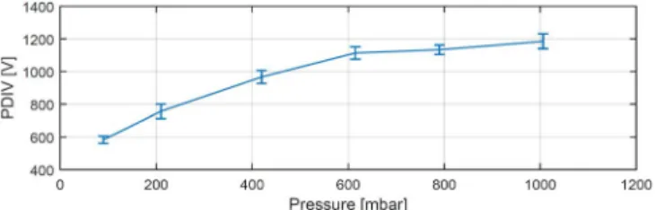
D. Aeronautic constraints: environmental pressure
Using the Paschen law, it is easy to prove that the PDIV of typical aeronautical EIS decreases drastically according to the pressure. Fig. 10 shows a measurements of PDIV versus pressure for the following setup: MW-0.71mm-G2 and 125μm polyimide paper.
Fig. 10. PDIV of MW-0.71mm-G2 & Polyimide paper 125µm vs. pressure The 100 mbar pressure reduces strongly the PDIV, to a 600V value, compared to 1150V at atmospheric pressure.
IV. CONCLUSION
In view of the different parametric studies presented in this paper: the new HVDC 540V aboard aircraft, combined with transient overvoltage along the harness and with low pressure aeronautical constraints can be fatal for the EIS type 1. Indeed, considering the overvoltages and insulation issues:
+ Overvoltages: The use of MOS-SiC technology increases
the mass density of ASD, but it also increases the motor overvoltages. The use of a shielded harness can generally avoid using the EMI filter at the output of the inverter, but our results show that shielding also contributes to the increase of motor overvoltages.
+ Type 1 EIS: When the motor PDIV is under overvoltages
level, in some cases, increasing the insulation thicknesses is potentially a simple solution which allows the ASD to become DP-free. In other specific cases, very low pressure for example, thicker insulation could not be sufficient and can impact the system from a thermal design point of view. So the reduction of overvoltages levels must be considered using adequate filter at inverter outputs or at motor terminals. The overvoltages and partial discharges are vital issues for the system’s lifetime and have to be considered from the early ASD design phases.
ACKNOWLEDGMENT
These works are conducted as a part of the FIABILITE project led by the Institute of Technological Research Saint Exupéry in collaboration with LAPLACE laboratory, AIRBUS Group, SAFRAN Group, ZODIAC AEROSPACE, LIEBHERR AEROSPACE and AEROCONSEIL. The authors would like to thank all the projects members for giving us permission to publish these works, their technical supports and discussions.
REFERENCES
[1] R. J. Kerkman, D. Leggate, and G. L. Skibinski, “Interaction of drive modulation and cable parameters on AC motor transients,”
IEEE Trans. Ind. Appl., vol. 33, no. 3, pp. 722–731, 1997.
[2] B. TAGHIA, B. COUGO, H. PIQUET, D. MALEC, A. BELINGER, and J. P. CARAYON, “Overvoltage at motor terminals in SiC-based PWM drives,” Elsevier Editor. Syst. Math.
Comput. Simul., 2018.
[3] P. Bidan, T. Lebey, G. Montseny, and J. Saint-Michel, “Transient voltage distribution in inverter fed motor windings: experimental study and modeling,” IEEE Trans. Power Electron., vol. 16, no. 1, pp. 92–100, 2001.
[4] J. . Bellomo, Lebey Thierry, F. Peltier, and J. . Oraison, “Conséquences des nouvelles formes de commande sur les matériaux de l’isolation statorique,” J.Phys. III Fr. 7, 1997. [5] T. Billard, C. Abadie, and B. Taghia, “Non-Intrusive Partial