HAL Id: hal-01214447
https://hal.archives-ouvertes.fr/hal-01214447
Submitted on 12 Oct 2015HAL is a multi-disciplinary open access
archive for the deposit and dissemination of sci-entific research documents, whether they are pub-lished or not. The documents may come from teaching and research institutions in France or abroad, or from public or private research centers.
L’archive ouverte pluridisciplinaire HAL, est destinée au dépôt et à la diffusion de documents scientifiques de niveau recherche, publiés ou non, émanant des établissements d’enseignement et de recherche français ou étrangers, des laboratoires publics ou privés.
Pb(Zr,Ti)03 ceramic thick films for optical device
applications
J. Cardin, D Leduc, C Boisrobert, H.W. Gundel
To cite this version:
J. Cardin, D Leduc, C Boisrobert, H.W. Gundel. Pb(Zr,Ti)03 ceramic thick films for optical device applications. SPIE Proceedings Series, 2003, 5122, pp.371-376. �10.1117/12.515798�. �hal-01214447�
Pb(Zr,Ti)03 ceramic thick films for optical device applications
J. Cardin, D. Leduc, C. Boisrobert, and H.W. Gundel*
Laboratoire de Physique des Isolants et d'Optronique EA 3254
(L.P.I.O.)
Université de Nantes, Nantes, France
ABSTRACT
Ferroelectric Pb,ZrTi1O3 (PZT) has been prepared by chemical solution deposition (CSD) and spin-coating technique, using acetate and alkoxide precursors. Rapid thermal annealing has been employed in order to obtain crystallization in the
perovskite phase. Aiming to study the optical properties of the films, PZT was deposited on different glass substrates.
Structural characterization ofthe films was done by X-ray diffraction, morphology was investigated by SEM micrography.
Using standard photography analysis, the films were qualified in terms of crack density, their appearance strongly
depending on the type of substrate. Using a visible to the near infrared spectrophotometer, the transmittance normal to the surface ofthe films was studied. Coupling oflaser light into the films by the M-lines technique allowed the determination of the refractive index and the thickness of the ferroelectric layer. A waveguiding interferometer structure of Mach-Zehnder type was realized by photolithography and wet chemical etching.
Keywords: PZT, thick films, glass substrate, transparency, M-lines, wet chemical etching, optical waveguide
1. INTRODUCTION
The improvement of optical networks for high bit rate telecommunication is mainly limited by the modulation and amplification stages of the light signal and hence new materials with improved properties are needed. An appropriate
material would have a high transparency in the visible and near infrared range, a strong refractive index, a high electro-optic response and a sufficient good long term stability.1'2 In order to realize a typical multi-layer waveguide structure, integration is necessary which also implies elaboration of the material by thin film techniques. Some ferroelectrics seem to meet this
criteria, like lithium niobate (LiNbO3) which is one of the most prominent member of this class of materials. Other
perovskite type ferroelectrics, like barium titanate (BaTiO3) or the large family ofPLZT solid solutions [(Pb,La)(Zr,Ti)03]
equally exhibit interesting properties for electro-optic applications.37 In the present study, we investigated the optical
properties oflead zirconate titanate (PZT) spin-coated on glass and the possibility to realize a Mach-Zehnder interferometer structure. The realization ofa PZT waveguide based on the use ofglass substrates would allow a future development of low cost devices which is ofhigh interest for telecommunication applications.
2. EXPERIMENTAL TECHNIQUE
The PZT thin films were elaborated by the Chemical Solution Deposition (C.S.D.) technique using a modified MOD Sol-gel process. The precursor solution was prepared at room atmosphere and temperature. In order to obtain PZT (36/64), lead acetate [Pb(CH3CO2)2,311201 was dissolved with an acetic acid solvent and an appropriate ratio between zirconium alkoxide [(Zr(C3H70)4)] and titanium n-propoxide [(Ti(C3H70)4)] adjusted. A 20 % lead excess was used in order to prevent losses during the annealing process, and ethylene glycol (HO-CH2-CH2-()H) was added to the solution in order to reduce cracking of the films.8 The final solution was filtered with a 200 nm seringe filter and was spin-coated onto the substrates at 2500 rpm duriig 20 seconds. Subsequently, the films were dried at 120°C and submitted to a rapid thermal annealing (RTA)
*
Correspondingauthors: Email: hartmut.gunde1physique.univ-nantes.fr; julien.cardinphysique.univ-nantes.fr;
httpi/www.sciences.univ-nantes.fr/physique/recherche/lpio;
Advanced Organic and Inorganic Optical Materials, Andris Krumins, Donats Millers, Inta Muzikante, Andris Sternbergs, Vismants Zauls, Editors, Proceedings of SPIE
Classical photolithography and wet chemical etching was employed for the realization of the waveguide structures,
using a mixture of 50 ml HC1 (37%), 50 ml HNO3 (69%) et
2 ml HF (48%) diluted to 50%. A detailed study on the
etching behavior of PZT ceramic thin films shall be
published elsewhere. 14The structural properties of the PZT films have
been determined by X-ray diffraction and
Scanning Electron Microscopy. MesOscopic
optical scanning ofthe films was performed with a
MINOLTA Dimage Dual Scan camera. The
optical transmittance, normal to the surface of the films, has been determined in a wavelength range
between 200 nm and 2 .tm with a CARY
spectrophotometer.40 45 50
20(°)
60 65 70
Figure 2: XRD pattern of PZT (36/64) films [, pyrochlore
phase, (xyz) perovskite phase)]
process during one minute. The crystallization behavior of the films was studied for different annealing temperatures,
ranging from 520°C to 620°C.
The PZT precursor solution was deposited on glass substrates of 25 x 25 mm2 area. Microscope slide glass was used in order to adjust the spin-coating parameters, and four types ofglass with different thermal properties were used in order to
study the filmability of the
material. Depending on the
spin-coating velocity, the thickness of one single layer ofPZT varied from 450 nm to
550 nm. Thicker films were
realized by multiple
spin-coating, including drying and
RTA heat treatment of each individual coating. The thermal properties ofthe substrates are shown in Table 1. As PZT has a linear thermal expansion coefficient of 5,5. 10, glass substrates with bigger and smaller coefficients were available.9
Table 1: Thermal properties ofthe glass substrates used for PZT thin film deposition
Substrate Schott D263T Schott AF45 Corning 7059 Corning 1737F
Coefficient oflinear
7,2.l0
4,5.10
4,6.l0
3,76.l0
thermal expansion (20°C-300°C) (20°C-300°C) (0°C-300°C) (0°C-300°C)
Strain point 529°C 627°C 565°C 666°C
Mirror
?J2 plate Beamsplitter Lense
Detector
He-Ne Laser
Motorized rotation stage
In order to determine the refractive index of the
PZT thin films, a M-lines measurement apparatus
was set up which applies the principle of
distributed coupling by evanescent fields to the
Figure 1: Schema ofthe rn-lines measurement set-up modes of the guiding structure.'° A ZnSe prism
having a refractive index higher than that of the ferroelectric, is pressed on the film (Figure 1) and is separated from it by a small air gap. The incident light is totally
reflected at the two sides ofthe prism, and leaves the prism parallel to the incident direction. For some angles of incidence, phase matching is obtained and coupling into the film due to
the evanescent field excited in the gap becomes possible.
Determination ofthese synchronous angles allows to find the
characteristic propagation constants of the film.'3 The
attenuated totally reflected light as a function ofthe angle of incidence constitutes a dark line spectrum. Variation of the
I
angle of incidence was performed by rotating the ensemblePZT/prism with a remote controlled motorized rotating
stage, synchronized to the detector (jthoto diode). The light
-sourcewas a He-Ne laser of 632.8 urn wavelength, and thepolarization of the incident beam was controlled by a half-wave plate associated to a polarizer.
20 25 30 35 55
3. EXPERIMENTAL RESULTS AND DISCUSSION
The development of the X-ray diffraction pattern of a 2 tm thick PZT (36/64) film deposited on a microscope slide glass substrate is shown in Figure 2 as a function ofthe annealing temperature. At 520°C, only a pyrochiore phase ofthe PZT can
be detected. With increasing annealing temperatures the respective peaks (at 20 29.5°, 34°, and 59°) decrease and are replaced by the perovskite pattern. At 580°C, the pyrochlore peaks become almost invisible. Starting from 600°C,
crystallization in the perovskite phase with a preferential (110) orientation ofthe film (20 31°) was obtained.
The microstructure ofthe PZT (36/64) films was studied by SEM technique in the normal secondary electron mode and the
backscattering mode. Figure 3 shows cross-sections of a 5-layer PZT film annealed at 620°C, resulting in an overall
thickness of approximately 2.7 tm. In the normal mode (Figure 3a), the typical PZT grain structure can be seen with the substrate on the right hand side of the photo. As the SEM picture was focussed to the PZT, the substrate does not appear clearly. Figure 3b was taken in the backscattering mode, where the brightness is proportional to the mass ofelements. At the
surface of the substrate, a brighter region of approximately 500 nm thickness is visible which should correspond to a
chemical element heavier than
glass. We suppose that
diffusion of lead from the
PZT to the substrate during
the thermal annealing process
causes this zone (diffusion
layer). 15
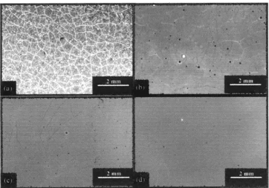
Themesoscopic structure of a
PZT mono-layer of
approxi-mately 450 nm thickness was
analyzed using optical
photography. In Figure 4,
deposition on four different glass substrates is compared. Figures 4a and 4b show the PZT films spin-coated on a Schott D263T and a Corning
7059 glass substrate,
presenting a high number of
cracks, respectively. In the
case of Figures 4c and 4d,
Schott AF45 and Corning
1737 glass substrates were
used, showing
a more
homogeneous surface with
considerably less cracks. Asthe cracks appear during
drying and annealing of the
films, we suppose that the
mismatch between the thermal properties of the glass and the
PZT film is at the origin of
this phenomenon. This maycause desiccation cracks during the drying process and strain cracks during annealing
and cooling of the films to
room temperature.
Figure 3: SEM micrographs of a PZT (36/64) film spin-coated on microscope slide glass. Cross-section (a) in the SEM normal mode and (b) in the backscattering mode
Figure 4: Optical photography of PZT films spin-coated on different glass substrates and annealed at 620°C, (a) Schott D 263, (b) Corning 7059, (c) Schott AF 45 and (d) Coming 1737F.
A!45
.
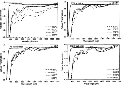
0,8 f -O,6 tO,4 IOptical transmission of a PZT mono-layer, deposited on the different glass substrates, is shown in Figure 5 for heat
treatment temperatures ranging from 560°C to 620°C. Transmission has been found to be between 30% and 80% in the visible wavelength range and up to 90% in the near infrared (2000 nm). In the case ofthe D263 glass substrate only, a lower transparency was observed for the films crystallized in the perovskite phase (600°C and 620°C). This is supposed to be due to light scattering, as in this case the PZT films show an overall inhomogeneous aspect with many mesoscopic cracks. The higher transparency of the same PZT film in the pyrochlore phase (560°C and 580°C)) where no cracks have been found,
confirms this assumption. The transmission spectra of the PZT films deposited on the 7059, AF45 and 1737F glass
substrates do not differ significantly. The UV cut offwavelength of the PZT is around 350 nm, respectively, corresponding to a band
750
gap energy of 3.5 eV, which is in accordance with the intrinsic
--. -..-..
limitoftransparency.'7 In the near infrared, and particularly at the
700 ••'••.-..•--.. -._•••\. ./_•••_•
"...-... "telecommunication
wavelength" (1 ,55 tim), transparency is almost
.. :
•-
that ofthe substrate.650
.
. .. 600 TE 550 d.k0.n12 (n sin 0m)2 arctan g12 sin93m2 2 _
aretang22
sinem 0:
m
=
0 (1)\
1 (n3 sm 03m) )\
1 (n3 sm 3m) )wherek0 is the wave vector and n0, n2, and n3 represent the refractive index of the substrate, the air gap, and the prism, respectively. The parameters gi and g2 are equal to one for TE polarization and equal to n1/n2 and n1/n0 for TM polarization.
D26 substrat 0,8 0 0,6 0 0,4 0. 0 0,2 0,0 I..' — —— Ii"
..
-I,. .,I
—— ——-580CC 560C 1,0 0,8 0 0,6 Co 04 00,2Unlike the case of metal
substrates,16 deposition on glass
resulted in more homogeneous
films with
less mesoscopic
cracks when the
thermalexpansion coefficient of the
substrate is smaller than that of
the PZT. This might be explained by the different thermal behavior
of the two types of substrate
during the annealing process.
Glass has a lower thermal
conductivity than metal, and theglass substrates used are thicker than the metal substrates
(0.7 mm and 0.2 mm). In the
case of the glasses investigated,homogeneous and crack-free
crystallization of the PZT filmswas favored by using the
substrate with the smallest
thermal expansion during the
RTA heat treatment process.
7059 substrat
- _—;
I,I
600CC I ..580*C 4 -..-. 560*C 400 600 800 1000 1200 1400 1600 1800 201 Wavelength(nm) 400 ' 600 ' 84;0 ' id®•ioo'1400 1600 1800 20 Wavetength(nm) DC 1,0 C0,8 0 0,6 Co 0,4 0 — — —620CC 600CC —. —- 580CC —"—. 560CC l737Fsubstrat . .r— ..
I i/'•.): ; I I ': I'
r I ———620CC 0,2 1 600CC . b —-—580C I-
"-. 560*C 0,0 -.--' 400 600 800 1000 1200 1400 1800 1800 200( Wavelength(nm) 400 600 800 10110 1200 14ó0 1600 1800 200C Wavelength (nm)Figure 5: Optical transmission ofPZT films prepared on different glass substrates and for different annealing temperature.
Co C 6) C 0) t a) a) -20 -19 -18 -17 -16 -15 -14 -13 Angle of incidence () Figure6: Typical TE dark line spectrum
A typical TE dark line spectrum from the PZT film obtained by the M-lines technique is presented in Figure 6. Two absorption lines
appears at an angle of approximately -16.7° and -13.9° and
correspond to the excitation oftwo guided modes in the film. -12 -11 -10 Therefractive index n1 and the thickness d ofthe ferroelectric film
are related to the synchronous angles O3andthe mode order m via the dispersion equation of a planar dielectric waveguide18
In order to determine n1 and d, equation (1) was solved numerically using a modified Newton-Raphson method.'9 In the case ofthe PZT film deposited on the 1737F glass substrate, a refractive index n1 =2.26 0.03 and a thickness d —2 0.2 Inn for a wavelength of 632 nm were obtained. The results are in good agreement with measurements at 1.3 jim and 1.55 iim wavelength (n1 =2.26and 2.20, respectively), obtained from the same film with a commercial measurement device.
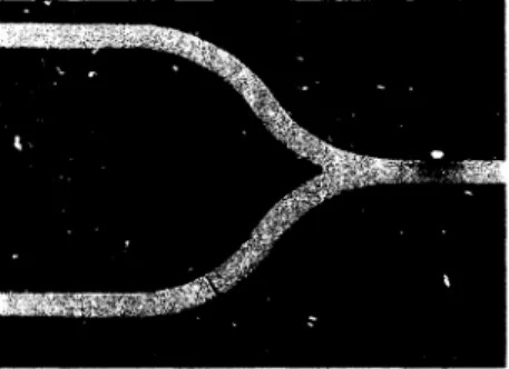
Figure 7: Optical photography ofa Mach-Zehnder interferometer structhre etched in a 2 jim thick PZT (36/64) film on glass substrate.
In order to study the possibility of using PZT films on glass substrates for waveguide applications, a Mach-Zehnder interferometer structure was realized by photolithography and wet chemical
etching, which is shown in Figure 7. A linear waveguide (left hand part of the structure) is split into two parallel branches (central part ofthe structure), one of which can be supplied with electrodes, in order to induce the electro-optic effects (linear Pockels effect or quadratic Kerr effect). Due to the resulting phase shift ofthe light with respect to the second branch, interference is obtained where the
branches are reunified (right hand part of the structure). The thickness of the PZT film is approximately 2 rim, the overall length of the interferometer structure is 14 mm. A SEM micrograph can be seen in Figure 8, showing the
right hand end ofthe two central branches ofthe interferometer. The width of the Figure 8: SEM micrograph of part of a
etched structure is approximately 30 j.tm. Light propagation within the
Mach-Zehnder interferometer. waveguide was observed qualitatively, but could not be recorded as yet.
4. CONCLUSIONS
PZT (36/64) films were realized by CSD, deposited by spin-coating on glass substrates, and a typical Mach-Zehnder
waveguide structure was obtained by wet chemical etching. While the grain structure ofthe ceramic type PZT thin film does not a priori hinder light propagation, up to now, macroscopic cracks in the ferroelectric layers did not allow a quantitative analysis ofthe attenuation in the guide. As could be shown, those cracks result from the different thermal behavior of the PZT and the glass substrate during the RTA heat treatment. For certain substrates, however, the PZT elaboration route
might be adapted in order to allow homogeneous and crack-free deposition of the films. The results from the optical
characterization ofthe films are encouraging for a future application in electro-optical devices. The transparency normal to
the surface is high at the telecommunication wavelength, and light propagation in the film over a few centimeters was
observed qualitatively. A M-lines measurement technique was set up which shall allow a more systematic study of the refractive index ofthe ferroelectric as a ftmction ofthe material composition and the preparation route parameters. A more profound knowledge on the related phenomena combined with the possibility of tailoring the refractive index of the films will be necessary to obtain monomode light propagation. Preliminary results on a wet chemical etched Mach-Zehnder type
interferometer structure show a sufficient good resolution in the micrometer region for a fimdamental investigation of light propagation in the PZT films and a future study ofthe electro-optic linear and non-linear effects.
ACKNOWLEDGMENT
The authors wish to thank Joel Charrier ofthe Laboratoire d'Optronique CNRS-UMR 6082 in Lannion, France, for helpful discussion and for the complementary M-lines measurements ofour PZT thin films.
REFERENCES
1. A. Carenco, "Composants actifs" in Systémes Optiques, G. Roblin (ed.), EDP Sciences, pp. 93-143, 1991.
2. J.P. Huignard, "Presentation de l'effet electro-optique", in Optoelectronique 1, P. Chavel, (ed.), EDP Sciences, pp. 289-294, 2002. 3. R.H. Kim, H.-H. Park, and G.-T. Joo, "The growth of LiNbO3 (006) on MgO (00&) and LiTaO3 (012) substrates by sol-gel
uoipmthd U!
UOOjqfl
'np
u
p"
U!pJ13 •f 61 6861'iZ68L6
-dd'sz
u'o
pa.ckI'SAM
POPPq
swjjj UqjO jo1dij,,'H
A'oji
j
'!1Id
i1 81 Z661'9Z1
dd',,z
.dOJcf dwa1'ao
•sa1wiv
'SWi!d U!q J2Nd PUiZid
'IZdJ°
SPd01d
'1U
WSP
'UID
-f
'Ud
HD L1 .ooo'soz-czo
dd'
•aowvjj
donj
f
'swiisqns
SSOJUS O1UO POIIPW jO-jOS icqsuijj
1°!fllZd
UflOO-tJflWJOuo!idJd,,
'PPUflD M'H'uq
j
j
'JJ1I4
'
f
'1.IoAyu
'u!Snmrid
'ouAs
a
91 666t'f-L
dd snippo.i.wj '<< SWIId u!uJIZd
J0 ws!tmt1oJAI UOiS1J&(I3 O14 uo sutdocjjo
oojjj
>>'is
NP
S)jOO49
)J 'IJflSS!IN UI
c1 ooug*Id 'pJtu!Q'oo
'8i-ct
iqop
'zoo
dDf SaflblJpa/aOJJdJ SadUZJ4 S'dljdflO3p
?UJflOJ JUOO 'UOtgO!1dd p!112AtM jRo!dooJ
swig u!qIZdJ°
U!qO
I0!Wl0
PM,, 'jpUflDMH
pu
'OUASI
'P°D
T
'U!pJRDf
'AIOAy cjL6J
'8O6iO6
dd'j
sipa-j pa.zckI'jdnoo
ws!JdqM
sioum.md wjguqjo
'OJOJ )J put qO.rjflJ
j
'uj
U!1,,
SAMu
uq
siujgiu
piu!
'so!do
pa!/dcIV'j
dd 'E1-c6Ez '1L61zi 0L61 'ocEL-LI dd