Science Arts & Métiers (SAM)
is an open access repository that collects the work of Arts et Métiers Institute of Technology researchers and makes it freely available over the web where possible.
This is an author-deposited version published in: https://sam.ensam.eu Handle ID: .http://hdl.handle.net/10985/7979
To cite this version :
Nesma NAFIE, Chedly BRAHAM, Mohamed BEN RABHA, Mongi BOUAICHA - Effect of the experimental parameters on the shape and formation kinetics of SiNWs formed by electroless chemical etching in aqueous AgNO3/HF/H2O2 solution - Physica Status Solidi C - Vol. 11, n°2, p.331-336 - 2014
Any correspondence concerning this service should be sent to the repository Administrator : archiveouverte@ensam.eu
on the shape and formation kinetics
of SiNWs formed by electroless chemical etching
in aqueous AgNO
3
/HF/H
2
O
2
solution
Nesma Nafie*,1, Chedly Braham2, Mohamed Ben Rabha1, and Mongi Bouaicha1
1 Laboratoire de Photovoltaïque, Centre de Recherches et des Technologies de l’Energie, Technopole de Borj-Cédria, BP 95,
Hammam-Lif, 2050 Tunis, Tunisia
2 Laboratoire Procédés et Ingénierie en Mécanique et Matériaux (Diffraction X) (UMR 8006), ENSAM, 151 BD de l’Hopital,
75013 Paris, France
Keywords silicon nanowires, etching parameters, formation kinetics
*Corresponding author: e-mail nesmanafie@yahoo.fr, Phone: (+216) 79 325 160, Fax: (+216) 79 325 825
The discovery at the beginning of 1990 of carbon nano-tubes awaked the interest for one-dimensional (1D) nanostructures. Currently, silicon nanowires (SiNWs) formed by electroless chemical etching in aqueous Ag-NO3/HF/H2O2 solution, arouse great interest due to their
physical properties and potential applications. The under-standing of physical-chemical phenomena that occur dur-ing the formation of SiNWs, the effect of etchdur-ing pa-rameters on their morphology, the formation mechanism and formation kinetic raise many questions. In this paper,
we investigate the effect of etching parameters; namely AgNO3 concentration, HF concentration, etching time
and the volume of H2O2 on the shape of obtained
nanos-tructures. The formation kinetic was investigated by studying the effect of the etching time on the morphology of obtained nanostructures. SiNWs studied in this work were formed on a P type and (100) oriented monocrystal-line silicon substrate. Characterization of formed SiNWs was performed using a scanning electron microscope (SEM).
1 Introduction
Metal-assisted electroless etching is one of top-down approaches that allow forming silicon nanostrures on sili-con wafer [1-3]. Depending on experimental parameters, porous Si with different morphologies, nanowires (SiNWs) as well as nanoholes of different shapes can be produced [1-4]. As a consequence of the geometrical dependence of physical and electrical properties of SiNWs based devices, it is very important to fabricate SiNWs in a well-controlled manner [5]. Hence, the study of the effect of electroless et-ching parameters on the shape of SiNWs becomes very in-teresting.
In this paper, we investigated the effect of the experi-mental parameters on the shape of silicon nanostructures fabricated by electroless chemical etching in aqueous
Ag-NO3/HF/H2O2 solution. The morphology of etched layers
formed on silicon was investigated by a scaning electron microscope (SEM).
2 Experimental process
SiNWs are prepared by silver assisted chemical etch-ing in HF aqueous solution [6-8]. We used boron-doped monocrystalline silicon, (100) oriented, with a thickness of 200 µm and a resistivity of 0.5-3.0 Ωcm. For the samples cleaning, we immerse them in a boiling acetone for 10 min and then in ethanol for 5 min to remove organic greases. After rinsing three times with de-ionized water (DIW), samples are etched in a 5% aqueous HF solution during 2 min to eliminate native silicon dioxides. After cleaning samples were immersed into the etching solution
contai-ning AgNO3 solution,10 ml aqueous HF solution and H2O2
at room temperature. After etching, to remove the silver
film, we immerse samples in HNO3 (44%) aqueous
332
3 Results: Effect of experimental parameters 3.1 Cleaning protocol
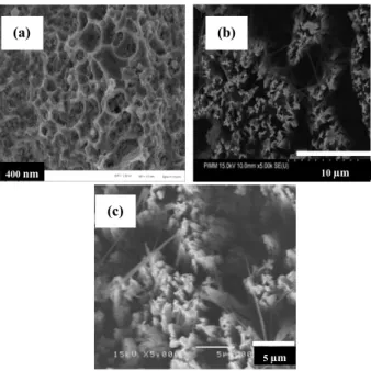
During etching, we remark that the cleaning step of Si samples influences the morphology of obtained nanostruc-tures. In Fig. 1, we give top SEM images performed on three samples. In Fig. 1(a), the sample was immersed in acetone during 5 min and in ethanol during 5 min. Then we immerse it in a sulfuric acid-hydrogen peroxide mixture
H2SO4 (97 %):H2O2 (30%) with a volume proportion 3:1
for 10 min. After that, the sample is rinsed with ultra-pure water, followed by a dipping in 5 % HF for 1 min and fi-nally rinsed with ultra-pure water. A second sample, which is imaged in Fig. 1(b), was immersed in a hydrochloric
ac-id- hydrogen peroxide mixture HCl (40%):H2O2 (30%)
with a volume proportion 1:1 for 8 min. Then, the sample was rinsed with ultra-pure water, and finally in acetone and isopropanol during 10 min each. The third sample (Fig. 1(c))) was immersed in a boiling acetone for 10 min then in ethanol for 5 min. After this step, the sample was rinsed three times with DIW. Finally, the sample was etched in a 5% aqueous HF solution for 2 min to eliminate native sili-con dioxide. All three samples were etched in a 40% HF
aqueous mixed with a 0.02 M AgNO3 aqueous solution for
60 minutes at ambient temperature. Regarding SEM im-ages of Fig. 1, one can notice that we obtain a porous like structure for sample corresponding to Fig. 1(a), however, for those of images (b) and (c), we obtain SiNWs. In addi-tion, we notice that SiNWs in Fig. 1(b) are homogeneous as compared to those obtained for the third sample (Fig. 1(c)). The latter difference in homogeneity is attributed to
the role of HCl:H2O2 in homogenizing the thickness of the
oxide layer, leading to a uniform etching of Si [9]. Ob-
tained results confirm the effect of the pre-surface treat-ment on the morphology of silicon nanostructures obtained by Shiu et al. [10].
3.2 Etching time
As compared to other etching processes, formation of SiNWs has a particular kinetic. The latter was investigated by studying the effect of the etching time on the morpho-logy of obtained silicon nanostructures. In Fig. 2, we give SEM images of formed SiNWs fabricated during 10, 20, 30, 40, 50 and 60 minutes in an etching solution mixed
with a 10 ml AgNO3 solution (0.050 M),10 ml aqueous HF
solution (40%) and 1 ml H2O2 (10.00 M). In each top
sur-face SEM image, we give in the upper right inset its cross-sectional SEM view. All top SEM images used in Fig. 2 were performed at the same magnification (x 10 000). We notice that SiNWs are formed uniformly. Cross-section images show that for short durations, SiNWs are not uni-form.
Using top SEM images of Fig. 2, we estimate values of the porosity by performing a fine mesh; Porosity is defined as the ratio of vacant cells by the total number of cells. In Fig. 3(a), we plot the shape of the porosity profile vs. etching time. Values of porosity vary in a relatively medium do-main: from 33 % to 68%. From cross-sectional SEM im-ages of Fig. 2, we measured the length of SiNWs, which we give in Fig. 3(b) as a function of the etching duration. As clearly seen in the cross-sectional SEM images of Fig. 2, the length of SiNWs is not homogeneous, for this reason we took three different values of length of nanowires, black dots correspond to the length of the shortest nano-wire, red dots correspond to the length of the average nanowire and green dots correspond to the length of the longest nanowires. Length of obtained SiNWs is plotted with error bars, where mean values vary from 11.5 µm to 25.8 µm. We notice that the length of SiNWs increases as the etching duration increases, according to the schemed curve shown with a blue line, which deviates slightly from the linear shape as obtained in references [5] and [11]. In Fig. 3(c), we plot the etching rate of Si vs. the etching time. We note that the etching rate decreases as the etching time increases. The etching rate was defined as the ratio of the SiNWs length by the etching time.
(a) 400 nm (b) 10 µm 5 µm (c)
Figure 1 Top surface of the SEM image of silicon
334 0 10 20 30 40 50 60 0 10 20 30 40 50 60 70 Po ro si ty ( % )
Etching time (min)
0 10 20 30 40 50 60 0 5 10 15 20 25 30 Si N W s a rr ay s L en g th ( μ m)
Etching time (min)
0 10 20 30 40 50 60 0,0 0,2 0,4 0,6 0,8 1,0 1,2 1,4 Et ch in g r at e ( μ m mi n -1)
E tching time (min)
Figure 3 Porosity (a), length (b) and etching rate (c) of SiNWs
vs. etching time. In (b) and (c), the blue lines were used to show the dependencies vs. etching time.
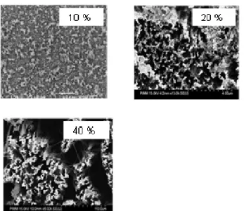
3.3 AgNO3 concentration
In this section, we discuss the effect of AgNO3
concentra-tion on the surface morphology of obtained SiNWs.
Sam-ples were etched in the AgNO3/HF (40%) solutions with 1
ml (10 M) H2O2, for 60 min. AgNO3 concentration was
va-ried from 0.010 to 0.050 mol/l.
After removing the silver films in nitric acid aqueous so-lution for several minutes, and rinsing samples with DIW, samples undergoe SEM investigation. In Fig. 4 we give the top SEM images of prepared samples, and, in Fig. 5, we give their cross-sectional SEM images. All top SEM views were performed at the same magnification (×2 000). Used
AgNO3 concentrations are M = 0.010, 0.015, 0.020, 0.025,
0.030, 0.035, 0.040, 0.045 and 0.050 mol/l.
Figure 4 Top surface SEM images of silicon nanostructures vs.
AgNO3 concentration.
(a)
(c) (b)
Figure 5 Cross-sectional SEM images of SiNWs vs. AgNO3
concentration.
According to the obtained SEM images, we obtain SiNWs for all concentrations. However, different shapes of the formed films can be observed. Hence, for samples
et-ched with AgNO3 concentrations; M=0.010; 0.025, 0.035,
0.040, 0.045 and 0.050 mol/l solutions, SiNWs are not homogenous. However, wires are well organized when
formed with an AgNO3 solution at concentrations 0.015,
0.020 and 0.030 mol/l.
Using SEM images of Fig. 5, we plot in Fig. 6 the
variation of the length of SiNWs vs. used AgNO3
concen-trations. Variation of the SiNWs length has an alternative behavior between formation and dissolution of wires.
Hen-ce, we obtain two intervals of AgNO3 concentrations for
which the SiNWs formation starts, and tow intervals for which the dissolution of wires begins. In addition, we
ob-tained values of the AgNO3 concentrations for which the
rate of SiNWs dissolution is very high.
0,005 0,010 0,015 0,020 0,025 0,030 0,035 0,040 0,045 0,050 0,055 10 15 20 25 30 Si N W s l en g th ( μ m)
AgNO3 concentration (mol/l)
Figure 6 Length of obtained SiNWs vs. AgNO3 concentration
(in mol/l).
3.4 HF concentration
To study the effect of the HF concentration on the morphology of obtained Si nanostructures, we etched Si samples in three HF aqueous solution; 10, 20 and 40%. Samples in this experiment were cleaned as follows: im-mersion in a hydrochloric acid- hydrogen peroxide mixture
HCl (40%): H2O2 (30%) at a volume proportion 1:1 for 8
min, then, they are rinsed with ultra-pure water, and finally immersed first in acetone and second in isopropanol during 10 min for each immersion.
After cleaning, silicon samples are immersed in a 10
ml aqueous AgNO3 solution (0.020 M) mixed with 10 ml
aqueous HF solution at different concentrations, for 60 min. After etching, the silver film was removed using a diluted
HNO3 (44%) aqueous solution for several minutes.
When the etching was processed in 10% HF solution, we obtain a pore formation on the Si sample as observed in Fig. 7. When HF concentration is increased to 20%, the density of the formed pores increases as observed in the middle image of Fig. 7. However, with a 40% HF etching solution, we obtained SiNWs.
Formation of SiNWs Dissolution of SiNWs starts High dis-solution of SiNWs New forma-tion of SiNWs Dissolu-tion of SiNWs starts
336
Figure 7 Top surface SEM images of Si nanostructures vs. HF
concentration.
3.5 H2O2 volume
In order to clarify the effect of the H2O2 oxidant agent
on the etching rate of silicon, two samples of (100) p-type Si of resistivity 1-2 Ω cm were etched in 10 ml aqueous
AgNO3 solution (0.02 M), 10 ml aqueous HF solution
(40%) and two different volumes of H2O2 (30%). The
et-ching duration is 30 minutes.
The left SEM image of Fig. 8 corresponds to a Si
sam-ple etched without additional oxidant (V(H2O2)=0 ml).
This image shows a formation of a superficial porous layer with an estimated thickness of about 1 µm at maximum.
When we add 10 ml of a H2O2 solution, we obtain a
mac-rospores structure as shown in the right SEM image. The thickness of the formed layer is about 11 µm. The latter va-lue was determined from the cross-section SEM view of this sample as given in the top right side of the correspon-ding image. Using these thicknesses, we assess that for
both cases; without and with H2O2, the etching rate is 0.05
and 0.36 µm min-1, respectively. Obtained values of the
et-ching rate are in accordance with the result obtained by au-thors of Ref. [12].
Figure 8 SEM images of silicon nanostructures vs. H2O2 volume.
4 Conclusion
In this work, we give results related to the effect of different experimental parameters influencing the shape and the kinetic formation of silicon nanostructures. Hence, we studied the effect of the cleaning protocol, the etching duration and the etchant concentration on the morphology of etched silicon layer. We pointed out that the morpholo-gy strongly depends on the etching parameters. We found that the pre-surface treatment influences the morphology of obtained silicon nanostructures. Under suitable experimen-tal conditions leading to the formation of SiNWs, we re-mark that the length of these wires increases when the time
etching was increaed. When we vary the AgNO3
con-centration, we obtain two intervals of AgNO3
concentrati-ons for which the SiNWs formation starts, and tow inter-vals for which the dissolution of wires begins. In addition,
we obtained values of the AgNO3 concentrations for which
the rate of SiNWs dissolution is very high. For the varia-tion of HF concentravaria-tion, no nanowires are formed at HF
concentration lower than 40%. For the effect of H2O2, we
found that when we add this oxidant agent to the etching solution, the etching rate of silicon increases considerably.
Acknowledgements Authors are grateful to the
Mitsubi-shi Corporation for the financial support in the form of a scholar-ship of 10 months, via a memorandum with the Ecopark of Sci-ence and Technology of Borj-Cedria, Tunisia.
References
[1] N. Megouda, T. Hadjersi, G. Piret, R. Boukherroub, and O. Elkechai, Appl. Surf. Sci. 255, 6210 (2009).
[2] N. Megouda, R. Douani, T. Hadjersi, and R. Boukherroub, J. Lumin. 129, 1750 (2009).
[3] K. Peng, J. Hu, Y. Yan, Y. Wu, H. Fang, Y. Xu, S.T. Lee, and J. Zhu, Adv. Funct. Mater. 16, 387 (2006).
[4] X. Li and P. W. Bohn, Appl. Phys. Lett. 77, 2572 (2000). [5] B. Ozdemir, M. Kulakci, R. Turan, and H. E. Unalan,
Nano-technology 22, 155606 (2011).
[6] N. Nafie, M. Abouda Lachiheb, and M. Bouaicha, Nanoscale Res. Lett. 7, 393 (2012).
[7] N. Nafie, M. Abouda Lachiheb, M. Ben Rabha, W Dimassi, and M. Bouaicha, Physica E 56, 427 (2014).
[8] M. Abouda Lachiheb, N. Nafie, and M. Bouaicha, Nanoscale Res. Lett. 7, 455 (2012).
[9] R. T. Tun, App. Phys. Lett. 68, 3461 (1996).
[10] S.-C. Shiu, S.-B. Lin, S.-C. Hung, and C.-F. Lin, Appl. Surf. Sci. 257, 1829 (2011).
[11] S.K. Srivastava, D. Kumar, P.K. Singh, M. Kar, V. Kumar, and M. Husain, Sol. Energy Mater. Sol. Cells 94, 1506 (2010).
[12] V. Lehmann (Wiley-VCH, 2002), p. 31.