INVESTIGATION OF THE ELECTRODEPOSITED ZnS NANOSTRUCTURES BY CHRONOAMPEROMETRY PROCESS: EFFECT OF THE ZINC SULFATE
CONCENTRATION
K. GHEZALI1,2,*, L. MENTAR 2, B. BOUDINE1 and A. AZIZI2
1
Laboratory of Crystallography, Department of Physics, University of Constantine, Road Ain El bey 25000, Algeria.
2
Laboratoire de Chimie, Ingénierie Moléculaire et Nanostructures, Université Ferhat Abbas-Sétif 1, 19000 Abbas-Sétif, Algeria.
ABSTRACT
Thin films semiconductor have widely been fabricated and improved to be used in photovoltaic application thanks to their special properties. Zinc sulfide (ZnS) present interesting properties, which give it place in solar cells application as window or buffer layer. ZnS thin films were prepared at room temperature by electrochemical deposition using zinc sulfate and sodium thiosulfate solution at pH 2.7. In this paper, we have investigated the influence of the zinc sulfate concentration on the structural, morphological and, optical properties for the electrodeposited ZnS thin films. SEM images demonstrated that the morphology of ZnS thin films depend greatly on the intial concentration of ZnSO4. XRD
studies confirmed the presence of zinc blende structure with the (200) orientation. The optical measurements (UV-Vis) show a large band gap between 3.4 –3.8 eV.
Keywords: XRD; thin films; nanostructures; carrier density.
Author Correspondence, e-mail: ghezali_khaoula1991@yahoo.com
1. INTRODUCTION
Photovoltaic is the direct conversion of light into electricity at the atomic level using semiconductor materials that exhibit the photovoltaic effect [1]. Semiconductors have widely been used in solar cells application such us Zinc sulfide .ZnS is used in junction with SnS[2], CuO [3] and CZTS[4],it is a potential candidate to replacing CdS in junction with CdTe and
CIGS [5], as buffer layer or as window layer in multilayer ZnS/CdS/CdTe solar cells [5]. ZnS present many interesting properties, essentially, high transparency, large band gap, n-type conductivity and high exciton binding energy (55meV) [3].
Zinc sulfide is a nontoxic, II–VI semiconductor, with a large direct band gap of about 3.7eV. ZnS has a refractive index (n) of 2.40 [3], which also make it suitbale for application as antireflective coatings in thin-film solar cells. ZnS has several advantages such as short-circuit current of the solar cell.
Different methods are used to elaborate ZnS thin films such as [6] Sol gel, spray pyrolysis, chemical vapor deposition, chemical bath deposition, pulsed laser and electrodeposition. The electrodeposition of thin films is considered as one of the promising ways due to possibility of controlling thickness, a deposition of large-area, a simple process, a low cost fabrication process and a good adhesion. There have been many work on the electrodeposition of ZnS, Most of the reported work on electrodeposition was done using the thiosulfate and zinc sulfate or zinc chloride as precursor for the electrodeposition of ZnS [5].
In the present work, we report the electrochemical synthesis of ZnS nanostructures on Indium tin oxide (ITO) conducting glass in acidic medium. Two different bath concentrations have been used. The electrochemical, structural, morphological and optical properties of ZnS nanostructures were studied to achieve ZnS nanostructures with High crystallinity quality.
2. RESULTS AND DISCUSSION
In our experiments, ZnS thin films were deposited cathodically on ITO glass substrate from zinc sulfate solutions. The general scheme of the electrodeposited ZnS thin films from sulfate bath are described in the previous study[7].
The reduction of thiosulfate ions generated the sulfur formation on the cathode as well as the acidic medium enhanced this reaction. Sulfur formation was presented in the following reaction [8]:
(1)
Also, Zinc ions are reduced on the ITO surface to the formation of ZnS nanostructure according to the following reactions [9];
(2)
The electrochemical mechanism of the electrodeposit ZnS from a sulfate solution was clearly described in the previous work [7].
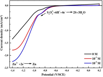
-1,4 -1,2 -1,0 -0,8 -0,6 -0,4 -0,2 0,0 0,2 -2,5 -2,0 -1,5 -1,0 -0,5 0,0 Zn2+ +2e- Zn S2O2-3+6H++4e- 2S+3H2O C u r r e n t d e n si ty ( m A /c m ²) 0 M 10-3 M 10-4 M Potential (V/SCE)
Fig. 1. Cyclic Voltammetry of aqueous solutions containing 10-3 M Na2S2O3 and a) 10-3 M, b)
10-4M of ZnSO4.
In order to study the electrochemical mechanism of ZnS thin films obtained on the ITO glass substrate at various ZnSO4 concentrations (0, 10-3 and 10-4 M), cyclic voltammetry
was used and the recorded voltammograms were presented in the figure.1. The potential range was varied between 0.2 and -1.4 V vs. SCE, bath temperature, pH and scan rate were fixed at 25 °C, 2.7 and 20 mV vs. SCE, respectively. Firstly, cyclic voltammetry of Na2S2O3 was
studied to give information about the cathodic reaction mechanism at the working electrode. In the absence of the Zn2+ ions, a small pic was observed at the range of -0.7 to -0.9 V attributed to the reduction of thiosulfate (Reaction 1), followed by a brutal drop in current due to the hydrogen evolution (H2) produced by the reduction of water according to the reaction.
In the presence of various Zn amount, the cathodic peak potential of the thiosulfate reduction shifted towards less negative values as the Zn concentration of the solution varied from 10-3 to 10-4 M. In addition, there is a simultaneously and relatively sharp increase of the cathodic current, this phenomenon implies catalytic role of Zn2+ to the reduction of thiosulfate. A second peak was observed in the range -1 to -1.4 V related to the reduction of
Zn2+ ions to the Zn metallic An increase of the cathodic current was observed when the ZnSO4 concentration was varies from 10-3 to 10-4 M. No major changes can be easily
observed in the voltammograms with varying zinc concentration.
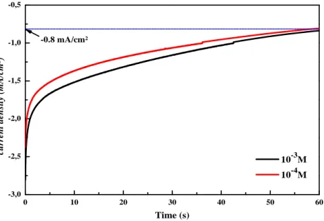
From the cyclic voltammetry experiments, we have chosen the cathodic potential for the formation of ZnS nanostructures. ZnS nanostructures was elaborated at different zinc concentration with potenstiostatic mod by imposing an applied potential of -1.2 V vs. SCE at the working electrode (which is our substrate ITO) for a duration of 5 min. A typical transient of an electrochemical process of three-dimensional nucleation-growth (3D) under diffusional control are characterized by a rapid decrease in current which corresponds to the charge of the double layer at the working electrode/electrolyte interface, and the time required for the formation of the first deposited nuclei on the surface [10]. Then, the current increases until reaching a maximum imax for a time equal to tmax. This is due to the growth of these nuclei and their recoveries [11]. Then the current decreases to a limit which is imposed by the diffusion of ions through the solution to the surface of the electrode
0 10 20 30 40 50 60 -3,0 -2,5 -2,0 -1,5 -1,0 -0,5 cu rr en t d en sit y (m A /c m ²) Time (s) 10-3M 10-4M -0.8 mA/cm²
Fig. 2. Experimental current transients of the electrodeposited ZnS on ITO at a) 10-3 and b) 10-4 M of ZnSO4.
Figure.2 presents the chronoamperometric curves of the ZnS thin films electrodeposited at various concentrations. A current value close to -2.75 mA was measured at the initial stage of the experiment corresponding to the current of the electrodeposition of the ZnS nanostructures on the ITO glass substrate. After a few seconds, the cathodic current start increasing to reach a maximum value at –0.8 mA, in those curves we didn't observe the
charge of the double layer at the beginning, because it’s very fast. Also, it is noted from this figure that the current density increases in proportional with the variation of zinc ions concentration from 10-3 to 10-4 M, due to the increase of the ionic conductivity.
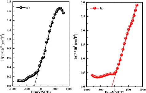
Mott-Schottky (M-S) analysis was employed for our thin films to study the effect of Zinc concentrations on the carrier density (ND) and flat band potential (Efb). Figure. 3 presents
M-S plots for the obtained ZnS thin films in 0.5 M of Na2SO4 as a supporting electrolyte, the
frequency was fixed at 800 Hz.
-1000 -500 0 500 1000 0,0 0,5 1,0 1,5 2,0 2,5 3,0 -1000 -500 0 500 1000 0,0 0,2 0,4 0,6 0,8 1,0 1,2 1,4 1,6 1,8 E(mV/SCE) b) 1 /C ² * 1 0 9 ( cm 4 F 2 ) 1 /C ² * 1 0 12 ( cm 4 F 2 ) E(mV/SCE) a)
Fig. 3. Mott-Schottky plots of the ZnS thin films deposited at a) 10-3M and b) 10-4M of ZnSO4 at 800 Hz.
All samples show positive slopes, indicating that those ZnS films are n-type semiconductors. The flat-band potential values obtained from the intercept at 1/C²= 0 at various Zn concentrations are reported to be -0.268 and -0.12 V vs. SCE. The donor carrier concentrations ND were calculated to be 1018 and 1021 cm-3 for the films deposited at 10-3 and
10-4 M of ZnSO4, respectively. We observe that ZnS thin films prepared at 10-4 M exhibited
higher donor density compared to ZnS prepared at 10-3 M. The presence of S-rich condition favor the formation of zinc antisites (ZnS) which leads an increase in the surface conductivity
[5],[12].
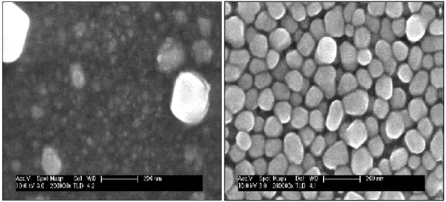
In order to study the effect of the Zn2+ ions concentrations on the morphological properties of the electrodeposited ZnS thin films on ITO-coated glass substrate at room temperature, the surface morphology of all samples was analyzed using SEM (Fig.4). From these figures, it is clearly that the film morphology is strongly influenced by changing the ZnSO4 concentration. The films deposited at high concentration 10-3 M show different size
and shape of grain and the polydispersed nature of the grain size could be due to an incomplete nucleation and particle growth rate. For the concentration 10-4 M, SEM image reveal uniform distribution of grains, the surface is partially covered by a coalescence of the crystallites to form relatively large aggregates with 3D growth (Fig 4).
Fig. 4. SEM images of the eclectrodeposited ZnS thin films from an aqueous solution
containing 10-3 M Na2S3O3 with various ZnSO4 concentrations: a) 10-3, b) 10-4 M.
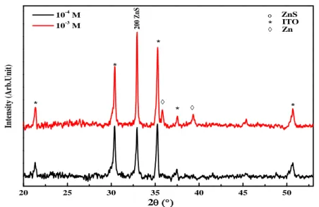
Figure. 5 shows the XRD spectra of samples prepared at two different concentration of ZnSO4. It can be seen that the deposited film shows a (200) preferred orientation for
zinc-blende phase of the obtained ZnS thin films, the intensity of the (200) peak increase inversely with the concentration, It is very strong and it width at half maximum (FWHM) is small, indicating a good crystallization state through a large crystallites size. Hence the apparition of Zinc impurity at 2θ= 35.74° and 39.39° correspond to (002) and (100) plan respectively is relative to low concentration of zinc sulfate [13]. While the samples deposited from aqueous solution containing 10-3 had no presence of impurity, these results confirm that obtained by MS measurements.
20 25 30 35 40 45 50 * * * * * o 2 10-4 M 10-3 M 200 Z nS ZnS * ITO Zn In te ns it y ( A rb .U ni t)
Fig. 5. XRD patterns of the ZnS thin films electrodeposited on ITO substrates at different Zn
concentration
The average crystallites sizes (D) has been calculated using the Scherrer’s equation and the corresponding values were given in table III.1.
Table 1. The effect of zinc sulfate concentration on the structural parameters of the
electrodeposited ZnS thin films.
samples 2ϴ(°) a(Å) D(nm)
10-4M 32.91 15.21 15.21
10-3M 32.93 18.58 18.58
It is quite clear that the average crystalline size of zinc sulfide increases with increased molar concentration of Zn2+ in the electrolyte. In addition, the lattice parameters of the cubic structure has been computed as 5.43 Å, which is very close to the values obtained in the literature [14]
Transmittance spectrums of ZnS films with two different concentrations of ZnSO4
recorded in the wavelength range from 250 to 800 nm was presented in the figure. 6-a. It is indicated that ZnS thin films exhibit a low transmittance values varied between 5 and 10 % in the visible range, which may be due to the presence of zinc in the films. These values are near to the values for ZnS derived from the electrochemical deposition process [15]. To improve the transparency of the obtained films several parameters is going to be discussed.
The optical band gap (Eg) for ZnS nanostructures was evaluated by using the Tauc
plot. The values of the optical band gap of ZnS layers is determined from the intercept of the straight-line portion at the horizontal axis when (αhυ)²= 0 (Fig. 6). the obtained Eg was 3.40
and 3.85 eV for the films deposited from solution containing 10-3 and 10-4 M ZnSO4
respectively. This augmentation in optical band gap is related to the defect presented in the obtained thin films.
1,5 2,0 2,5 3,0 3,5 4,0 300 400 500 600 700 800 0 2 4 6 8 10 12 h )² ( u a ) Eg(eV) a b b) T (% ) (nm) A B a)
Fig. 6. a) transmittance spectrum, b) (αhυ)2 vs. energy dependence for the determination of
the optical band gap energy of ZnS thin films on ITO-coated conducting glass surfaces obtained at different ZnSO4 concentrations.
3. EXPERIMENTAL
ZnS films was carried out in a glass three-electrode cell equipped with a saturated calomel electrode (SCE) placed as a reference electrode, platinum plate as a counter electrode and Indium tin oxide (ITO) coated glass substrates as the working electrode. The ITO substrates were ultrasonically cleaned with acetone, methanol and distillate water for 10 min, respectively and then dried in the air. ZnS thin films were electrodeposited potentiostatically from solution contained 10-4M of Na2S2O3, 10-3 and 10-4 M of ZnSO4. the pH was adjusted to
be 2.7 using diluted H2SO4. Films were deposited at potential -1.2vs.SCE using
Potentiostat/Galvanostat (PGZ301, Radiometer Analytical). After deposition, the films were rinsed with distillate water and dried in the air.
The surface morphology and microstructure of the ZnS nanostrutures were examined using scanning electron microscopy (SEM) JEOL 7800F. Phases identification and crystallographic structure determination were carried out using XRD Bruker AXS D8 Discover with CuKa1 radiation (k = 1.5418 Å) in a - 2 geometry. The optical properties were observed by UV-Visible spectroscopy JASCO V-670 UV-Vis.
4. CONCLUSION
In this work we have presented an electrochemical deposition and properties of ZnS thin films on ITO surfaces from aqueous zinc sulfate bath, we had investigated the effect of ZnSO4 concentration on electrodeposition process, morphological, structural and optical properties of ZnS. The SEM study shows that varying ZnSO4 concentration has a great influence on the morphological and grain size, XRD show a blend phase structure at room temperature, Mott-Schottky confirm the n type conductivity and the UV-Vis how a high band gap which makes it suitable to use as a widow layer in solar cell application.
5. REFERENCES
[1] D. Rekioua and E. Matagne, Optimization of photovoltaic power systems: Modelization, Simulation and Control, vol. 102. 2012.
[2] M. B. Dergacheva, K. A. Urazov, G. M. Khussurova, and K. A. Leontyeva, “New Method of Pulsed Electrodeposition of Nanostructure of ZnS Films,” Coatings, vol. 6, no. 2, p. 14, 2016.
[3] N. Lehraki, M. S. Aida, S. Abed, N. Attaf, A. Attaf, and M. Poulain, “ZnO thin films deposition by spray pyrolysis: Influence of precursor solution properties,” Curr. Appl. Phys., vol. 12, no. 5, pp. 1283–1287, 2012.
[4] A. I. Inamdar, K.-Y. Jeon, H. S. Woo, W. Jung, H. Im, and H. Kim, “Controlled growth of Cu2ZnSnS4 (CZTS) thin films for heterojunction solar-cell applications,” J. Korean Phys. Soc., vol. 60, no. 10, pp. 1730–1734, 2012.
[5] O. K. Echendu, A. R. Weerasinghe, D. G. Diso, and F. Fauzi, “Characterization of n -Type and p --Type ZnS Thin Layers Grown by an Electrochemical Method,” vol. 42, no. 4, pp. 692–700, 2013.
[6] J. Liu, A. Wei, and Y. Zhao, “Effect of different complexing agents on the properties of chemical-bath-deposited ZnS thin films,” J. Alloys Compd., vol. 588, pp. 228–234, 2014.
[7] K. Ghezali, L. Mentar, B. Boudine, and A. Azizi, “Electrochemical deposition of ZnS thin films and their structural, morphological and optical properties,” J. Electroanal. Chem., vol. 794, 2017.
[8] X. Xu, F. Wang, Z. Li, J. Liu, J. Ji, and J. Chen, “Effect of sulfosalicylic acid (C7H6O6S) on the electrodeposition of pure ZnS nanocrystal thin films from acidic solutions,” Electrochim. Acta, vol. 87, pp. 511–517, 2013.
[9] J. Y. Liao and K. C. Ho, “A photovoltaic cell incorporating a dye-sensitized ZnS/ZnO composite thin film and a hole-injecting PEDOT layer,” Sol. Energy Mater. Sol. Cells, vol. 86, no. 2, pp. 229–241, 2005.
[10] M. R. Khelladi, L. Mentar, A. Beniaiche, L. Makhloufi, and A. Azizi, “A study on electrodeposited zinc oxide nanostructures,” J. Mater. Sci. Mater. Electron., vol. 24, no. 1, pp. 153–159, 2013.
[11] L. Mentar et al., “Effect of nitrate concentration on the electrochemical growth and properties of ZnO nanostructures,” J. Mater. Sci. Mater. Electron., vol. 26, no. 2, pp. 1217– 1224, 2014.
[12] A. NICOARA, “Mott-Schottky analysis of electrodeposited ZnS thin films A,” Stud. Univ. babes-bolyai, Chem. LIII, 1, 2008.
[13] H. M. M. N. Hennayaka and H. S. Lee, “Structural and optical properties of ZnS thin film grown by pulsed electrodeposition,” Thin Solid Films, vol. 548, pp. 86–90, 2013.
[14] J. L. Birman, “Electronic energy bands in ZnS: Potential in zincblende and wurtzite,” Phys. Rev., vol. 109, no. 3, pp. 810–817, 1958.
[15] X. Xu, F. Wang, J. Liu, Z. Li, J. Ji, and J. Chen, “Structural and optical studies of ZnS nanocrystal films prepared by sulfosalicylic acid (C 7H 6O 6S)-assisted galvanostatic deposition with subsequent annealing,” Thin Solid Films, vol. 520, no. 23, pp. 6864–6868, 2012.