Publisher’s version / Version de l'éditeur:
Accounts of Chemical Research, 50, 10, pp. 2479-2486, 2017-09-13
READ THESE TERMS AND CONDITIONS CAREFULLY BEFORE USING THIS WEBSITE.
https://nrc-publications.canada.ca/eng/copyright
Vous avez des questions? Nous pouvons vous aider. Pour communiquer directement avec un auteur, consultez la première page de la revue dans laquelle son article a été publié afin de trouver ses coordonnées. Si vous n’arrivez pas à les repérer, communiquez avec nous à [email protected].
Questions? Contact the NRC Publications Archive team at
[email protected]. If you wish to email the authors directly, please see the first page of the publication for their contact information.
NRC Publications Archive
Archives des publications du CNRC
This publication could be one of several versions: author’s original, accepted manuscript or the publisher’s version. / La version de cette publication peut être l’une des suivantes : la version prépublication de l’auteur, la version acceptée du manuscrit ou la version de l’éditeur.
For the publisher’s version, please access the DOI link below./ Pour consulter la version de l’éditeur, utilisez le lien DOI ci-dessous.
https://doi.org/10.1021/acs.accounts.7b00234
Access and use of this website and the material on it are subject to the Terms and Conditions set forth at
High-purity semiconducting single-walled carbon nanotubes: a key
enabling material in emerging electronics
Lefebvre, Jacques; Ding, Jianfu; Li, Zhao; Finnie, Paul; Lopinski, Gregory;
Malenfant, Patrick R. L.
https://publications-cnrc.canada.ca/fra/droits
L’accès à ce site Web et l’utilisation de son contenu sont assujettis aux conditions présentées dans le site LISEZ CES CONDITIONS ATTENTIVEMENT AVANT D’UTILISER CE SITE WEB.
NRC Publications Record / Notice d'Archives des publications de CNRC:
https://nrc-publications.canada.ca/eng/view/object/?id=6c5e34f4-1e3e-4cc9-acbf-5f55aea064bd https://publications-cnrc.canada.ca/fra/voir/objet/?id=6c5e34f4-1e3e-4cc9-acbf-5f55aea064bd
High-Purity Semiconducting Single-Walled Carbon Nanotubes: A Key
Enabling Material in Emerging Electronics
Jacques Lefebvre,
*
Jianfu Ding, Zhao Li, Paul Finnie, Gregory Lopinski, and Patrick R. L. Malenfant
*
National Research Council of Canada, Ottawa, Ontario, Canada K1A 0R6
CONSPECTUS: Semiconducting single-walled carbon nanotubes (sc-SWCNTs) are emerging as a promising material for high-performance, high-density devices as well as low-cost, large-area macroelectronics produced via additive manufacturing methods such as roll-to-roll printing. Proof-of-concept demonstrations have indicated the potential of sc-SWCNTs for digital electronics, radiofrequency circuits, radiation hard memory, improved sensors, and flexible, stretchable, conformable electronics. Advances toward commercial applications bring numerous opportunities in SWCNT materials development and characterization as well as fabrication processes and printing technologies.
Commercialization in electronics will require large quantities of sc-SWCNTs, and the challenge for materials science is the development of scalable synthesis, purifi-cation, and enrichment methods. While a few synthesis routes have shown promising results in making near-monochiral SWCNTs, gram quantities are available only for
small-diameter sc-SWCNTs, which underperform in transistors. Most synthesis routes yield mixtures of SWCNTs, typically 30% metallic and 70% semiconducting, necessitating the extraction of sc-SWCNTs from their metallic counterparts in high purity using scalable postsynthetic methods. Numerous routes to obtain high-purity sc-SWCNTs from raw soot have been developed, including density-gradient ultracentrifugation, chromatography, aqueous two-phase extraction, and selective DNA or polymer wrapping. By these methods (termed sorting or enrichment), >99% sc-SWCNT content can be achieved. Currently, all of these approaches have drawbacks and limitations with respect to electronics applications, such as excessive dilution, expensive consumables, and high ionic impurity content. Excess amount of dispersant is a common challenge that hinders direct inclusion of sc-SWCNTs into electronic devices. At present, conjugated polymer extraction may represent the most practical route to
sc-SWCNTs. By the use of polymers with a π-conjugated backbone, sc-SWCNTs with >99.9% purity can be dispersed in organic
solvents via a simple sonication and centrifugation process. With 1000 times less excipient and the flexibility to accommodate a broad range of solvents via diverse polymer constructs, inks are readily deployable in solution-based fabrication processes such as aerosol spray, inkjet, and gravure. Further gains in sc-SWCNT purity, among other attributes, are possible with a better understanding of the structure−property relationships that govern conjugated polymer extraction.
This Account covers three interlinked topics in SWCNT electronics: metrology, enrichment, and SWCNT transistors fabricated via solution processes. First, we describe how spectroscopic techniques such as optical absorption, fluorescence, and Raman spectroscopy are applied for sc-SWCNT purity assessment. Stringent requirements for sc-SWCNTs in electronics are pushing the techniques to new levels while serving as an important driver toward the development of quantitative metrology. Next, we highlight recent progress in understanding the sc-SWCNT enrichment process using conjugated polymers, with special consideration given to the effect of doping on the mechanism. Finally, developments in sc-SWCNT-based electronics are described, with emphasis on the performance of transistors utilizing random networks of sc-SWCNTs as the semiconducting channel material. Challenges and advances associated with using polymer-based dielectrics in the unique context of sc-SWCNT transistors are presented. Such transistor packages have enabled the realization of fully printed transistors as well as transparent and even stretchable transistors as a result of the unique and excellent electrical and mechanical properties of sc-SWCNTs.
■
OPTICAL METROLOGY FORSEMICONDUCTOR-ENRICHED CARBON NANOTUBES
Applications in printable or high-end electronics will require bulk-scale synthesis of single-walled carbon nanotubes (SWCNTs). Currently, such methods produce a mixture of semiconducting (sc) and metallic (m) types, and for many devices,1−3
the presence of
m-SWCNTs severely degrades the electronic performance.
Although a number of lab-scale methods can efficiently remove
m-SWCNTs in devices, commercially viable approaches are
needed, especially in printable electronics, where low cost and high throughput are required. There, solution-phase processes are better-suited and can produce dispersions that are highly enriched with sc-SWCNTs. Progress on improving the m/sc purity to a target level, say 99% or 99.9999%, has become a metrological challenge, even at modest purity levels, and char-acterization tools and analysis methods are needed to support materials improvement. For R&D, optical tools are ideal, providing
Received: May 9, 2017
Published: September 13, 2017
pubs.acs.org/accounts
Published 2017 by the American Chemical
both rapid and accurate feedback. Although they are generally not quantitative, optical methods can discriminate between two samples of different m/sc purity. In addition to being efficient, they are nondestructive and can be used on macroscopic or microscopic length scales.
This section covers optical metrology tools that we routinely use to guide SWCNT enrichment using conjugated polymer extraction.4−8 Ultraviolet−visible−near-infrared (UV−vis− NIR) optical absorption, Raman scattering spectroscopy and imaging, and photoluminescence excitation spectroscopy will be described with an emphasis on their strengths and limitations with respect to today’s ultrahigh-purity sc-SWCNTs.
The power of optical metrology lies in the fact that SWCNTs have characteristic optical transitions in the UV, visible, and NIR ranges. For each SWCNT with a specific diameter and chirality, these transitions are unique and spectrally narrow. Metallic or quasi-metallic SWCNTs have a continuum of excitations with a prominent interband resonance (M11) in the visible region for the 0.9−1.5 nm diameter range. sc-SWNCTs have optical resonances (labeled S11, S22, S33, and S44) spanning a large spectral range from 400 to 2500 nm. At shorter wavelengths, optical transitions for both m- and sc-SWCNTs overlap strongly with a plasmon mode.
As shown in Figure 1, optical absorption captures these transitions well. The relative intensities of the assigned peaks
relative to background can serve to assess the purity.9 For SWCNT enrichment (0.9−1.5 nm diameter range) with conjugated polymers, a metric ϕ can be used to track the
sc purity. As highlighted inFigure 1a, ACNT and AB, the two
integrated areas extracted from a spectrum, are used to calculate the ratio ϕ = ACNT/(ACNT + AB). For SWCNTs inFigure 1a,
ϕranges between 0.06 for unprocessed material and 0.42 at high
sc purity. Values greater than 0.40 are expected when purity
beyond ∼99.5% is achieved. ϕ relates specifically to a given SWCNT population with its own diameter and chirality distri-bution. While similar figures of merit can be defined for smaller-diameter SWCNTs obtained from CoMoCat or HiPCO synthesis, comparison between different source materials is not trivial.
Nowadays sc purities in excess of 99.9% can be readily achieved, and optical absorption provides limited feedback on enrichment process improvements. Raman scattering, however,
has characteristic features that can be used to track sc purity. The radial breathing mode (RBM) region (∼100−300 cm−1) is
commonly used for qualitative m/sc purity assessment. As shown inFigure 1b, marked differences in RBM intensity are observed for unprocessed and enriched materials. It may be tempting to define an RBM figure of merit; however, the RBM intensity depends strongly on the choice of laser wavelength,10and only a small subset of the SWCNT population is sampled (four to six individual SWCNT species out of >20, typical of larger-diameter distributions). Proper metrological assessment using RBM intensities as a metric requires multiwavelength spectroscopy.11,12 In contrast, the G band is much less sensitive to the choice of laser wavelength, and with more species being sampled, a good representation of the SWCNT population is obtained.13,14 Although this Raman mode is common to all forms of sp2
-bonded carbons, the intensity in SWCNTs is enhanced by the resonant nature of the process (i.e., the laser matches an optical transition, typically S22 or M11). The G band in SWCNTs also carries a spectral signature unique to m-SWCNTs. Figure 1c shows the Raman signal obtained under resonant excitation with
M11. The G−
band is broad, asymmetric, and red-shifted away from the G+band in the unprocessed material. For material that is highly enriched in semiconductor nanotubes, the G−
band is still visible but is strongly suppressed. Similar to optical absorption, a figure of merit can be defined to track the sc purity beyond 99%.15 This could be conveniently used for process monitoring, even in situ and in real time by adapting techniques we have developed.16A limit of bulk spectroscopic methods such as this is set by the fact that the spectrum of the majority species (sc-SWCNTs) eventually overlaps significantly with that of the minority species (m-SWCNTs), even if the former is off-resonance. Thus, even though m-SWCNTs are resonant, the G−
band in Figure 1c (633 nm) has a primarily sc line shape. Moreover, the
m content is low enough that the wrapping polymer (e.g.,
poly(9,9-di-n-dodecylfluorene) (PFDD)) contributes signifi-cantly to the G+peak (the high-frequency shoulder).
Optical techniques are essential to qualify material at the semiquantitative level and could provide quantitative outputs if physical constants are known for every (n,m) species.17,18 Alternatively, Raman scattering can focus on individual nanotube detection and use counting and statistics to quantify the purity. Raman-based counting techniques can accurately build up statistics19and provide a sc purity for trace m-SWCNT content in thin films, such as in transistors.20Since nanotube adhesion is often selective, this method provides direct information from the layers in a device.21 With their specific G-band signature,
m-SWCNTs are spectrally and spatially identified in high-density
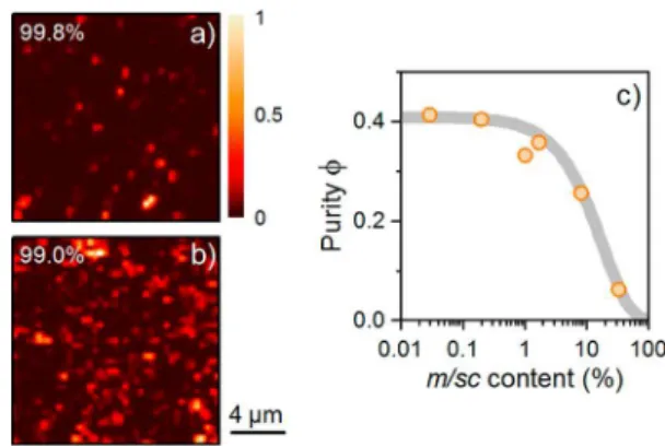
networks composed mainly of sc-SWCNTs. Under resonant excitation with m-SWCNTs, spatial maps are generated using G-band and RBM Raman spectra (Figure 2a,b), and pixels of high intensity are counted to obtain an absolute purity number (given a known SWCNT surface coverage). Purities in excess of 96% can be obtained with the method, and at the highest purity levels, meaningful statistics requires sampling large enough areas. Purity numbers from counting correlate well with absorption spectroscopy and transistor performance. Figure 2c shows a correlation between ϕ and Raman m/sc content. The observed saturation determines the limit of optical absorption in discrim-inating between materials with sc purities beyond ∼99.5%.
Along with m/sc purity, the need to determine the abundance and purity of specific SWCNT diameter/chirality is growing. Photoluminescence (PL) and Raman excitation mapping are useful methods because of their species selectivity.10,22The two Figure 1. Optical characterization of SWCNTs (unprocessed and
enriched using conjugated polymers) by (a) optical absorption and (b, c) Raman spectroscopy in the RBM and G-band ranges.
Accounts of Chemical Research Article
DOI:10.1021/acs.accounts.7b00234
Acc. Chem. Res. 2017, 50, 2479−2486
methods are broadly similar and provide complementary infor-mation with different strengths and weaknesses. With a tunable light source, a set of spectra is acquired for a range of excitation wavelengths, and the spectra are collated to produce an intensity map. As shown inFigure 3a, a PL map produces a pattern of spots
from S22 and S11 transitions, with each spot assigned to a given (n,m) species (Figure 3b). For a Raman map, a pattern of spots arises from S22 and RBMs or M11 and RBMs. Both PL and Raman methods can confirm the presence of specific (n,m) species in a sample. However, statements about the absence of a given species should be made with caution: m-SWCNTs that are always “dark” in PL, meaning they provide no signal, are an obvious example. Other SWCNT(n,m) may be dark as well for other considerations, intrinsic or extrinsic. As a general rule, the intensities for each (n,m) species in PL and Raman maps are different. Even if the species is the most abundant one in a sample, the corresponding peak may not always be the brightest. InFigure 3a, at least nine different peaks can be identified, and although the (10,9) chirality is seemingly the dominant one, an absolute cross section for individual SWCNT species is required to quantify the abundance.
For all three optical methods, population analysis can be affected by factors including length, defects, bundling, and doping. To some extent, all of these factors possess some degree of diameter/chirality dependence. The use of any figure of merit should constantly be validated with a critical assessment of
spectral changes that might occur following material processing. For example, bundling is understood to give rise to a featureless background in optical absorption, mode enhancement/suppres-sion in Raman,23and efficient energy transfer in luminescence.24 In a PL spectrum such as the one inFigure 3c, little difference is found compared to optical absorption, indicating that sc-SWCNTs obtained with conjugated polymer extraction contain few bundles.25
■
MUSINGS ON sc-SWCNT ENRICHMENT WITH CONJUGATED POLYMERSConjugated polymer extraction is a simple process in which conjugated polymers are used to selectively disperse sc-SWCNTs in organic solvents, after which m-SWCNTs are easily removed via centrifugation. The process is comparatively efficient, in which hundreds of milligrams can be isolated in hours using lab-scale dispersion and centrifugation equipment. High-sc-purity SWCNT dispersions are readily obtained with a variety of conju-gated polymers, including fluorene,4,5,26,27 thiophene,28 and carbazole29constructs.30When polymers comprising common conjugated building blocks such as those mentioned above are used, the economics of the process are favorable, with $5 per milligram feasible based on materials costs alone. The ability to cover ≫10 m2with 1 mg of nanotubes using digital printing
techniques makes this material very competitive compared with both organic and inorganic semiconductors. With the conjugated polymer in hand, the enrichment, spectroscopic characterization, and device printing can be accomplished in a day’s work, given that the final product is readily dispersed in common organic solvents, thus resulting in a printable ink directly from the enrichment process. As the topic of enrichment has recently been reviewed by others,6−8,30
we focus the present discussion on emerging trends and the effect of doping on the enrichment mechanism.
Our effort has focused mainly on “larger-diameter” SWCNTs (d > 1.0 nm, obtained using arc-, laser-, or plasma-based31 synthetic methods), with the expectation of superior electrical performance.32For a broad distribution (0.8−2.0 nm diameter, with all chirality and electronic types), selectivity is understood to originate from the proper combination of conjugated polymer backbone, side-chain length, solvent polarity, density, and viscosity,33−35
with supporting evidence that copolymers are very effective with larger-diameter SWCNTs.36,37Mistry et al.36 provided great insight into the extraction of large-diameter
sc-SWCNTs with >99% purity using
poly[(9,9-dioctylfluorenyl-2,7-diyl)-alt-co-(6,6′-{2,2′-bipyridine})](PFO-BPy), making a strong case for obtaining simultaneously higher yields and purities compared with aqueous-based techniques. Loi’s group demonstrated that the diameter selectivity of polyfluorene homopolymers can be tuned by varying the length of the alkyl side chain, and upon going from eight to 18 carbons, the larger-diameter nanotubes (from 0.75 to 1.51 nm) become more pronounced in the dispersion.6 Until this disclosure, it was believed that polyfluorene homopolymers were limited to dispersing smaller-diameter nanotubes. In either case, near-armchair sc-SWCNTs are mostly extracted using polyflurene-based polymers. Our own efforts with polyfluorene homopol-ymers are consistent with these reports: excellent purities and maximized yields (vide infra) are achieved when the polymer molecular weight is >10 000.25
On the basis of optical absorption and the ϕ purity metric, various trends as functions of process parameters can be found. Figure 4 summarizes some important observations that are Figure 2. Determination of sc purity using Raman spatial mapping
(633 nm excitation). (a, b) G−
intensity maps using SWCNTs with two sc purities. (c) Relationship between the ϕ value (from optical absorption) and Raman-based m-SWCNT content determined by nanotube counting.
Figure 3.(a) PL excitation map from sc-SWCNTs. (b) (n,m) species assignment for the data set in (a). (c) Comparison between luminescence and optical absorption.
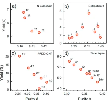
generally true for conjugated polymer extraction: Polymers with alkyl side chain lengths of C10 or greater are needed when
targeting larger-diameter species, yet we observe no discernible trend in the yield as a function of chain length; more careful studies on the effects of molecular weight and polydispersity are warranted (Figure 4a). Multiple extractions can be used to promote yields up to 20%, but the sc purity will be compromised, which may degrade the electronic performance. We use extraction number 4 among the eight depicted inFigure 4b to illustrate the fact that the yield may be improved simply by lowering the concentration and increasing the polymer/SWCNT ratio of the dispersion. Lower polymer/SWCNT ratios provide higher purities at the expense of yield (Figure 4c). m-SWCNT aggregation is also an important factor when balancing trade-offs between purity and efficiency (Figure 4d). It is a slow process spanning minutes to hours, a mechanism that was tested by
applying a second centrifugation step to the original supernatant while varying the time lapse between the two centrifugations. Additives such as silica gel can expedite sedimentation into
m-SWCNT-rich aggregates while further promoting sc purity
(>99.9%) and improving the yield.38 Incorporation of heterocyclic comonomers such as pyridines/bipyridines into polyfluorenes enables the use of shorter side chains while providing similarly high purities with improved yields and excellent colloidal stability, effectively mitigating SWCNT bundling in purified samples during device fabrication.30,39
The consensus regarding selectivity is that the mechanism is largely governed by the polymer structure, the solvent type, and the polarizability differences between m- and sc-SWCNTs, which result in different colloidal stabilities for the respective SWCNT−polymer complexes. Recent developments indicated that this effect is enhanced by nanotube doping,40 providing insight into the mechanism by demonstrating the effect of using water to improve the selectivity while also using vitamin E as a reducing agent to mitigate the selectivity. Redox effects are equally important in other enrichment methods, such as two-phase extraction.41
SWCNT doping occurs in the presence oxygen/water and affects the electronic and spectroscopic properties of SWCNTs. This redox process is also strongly pH-dependent as depicted in Figure 5.42−45
While developing our process, we observed variations in the yield and purity as functions of acid/base treatments prior to the enrichment steps. In a series of experiments, the influence of pH on conjugated polymer extraction and its effect on the m/sc selectivity were examined by treating raw SWCNTs with acid and subsequently titrating with base.46Figure 5a shows the correlation between sc purity and added hydroxide ions per nanotube carbon. Such treatment mitigates surface pH, significantly increasing the extraction yield and dramatically degrading the sc purity. This is attributed to reduced p doping at high pH, which results in reduced bundling interactions with m-SWCNTs, as illustrated in Figure 5b. The higher polarizability of m-SWCNTs and its effect on their selective assembly into unstable colloids is mitigated by eliminating the presence of doping (charged species) on the surface of sc-SWCNTs at higher pH. It is striking to see inFigure 5a how the transition from high to low sc purity is manifested as a function of reduced doping (a consequence of the tunable redox Figure 4.Plots of yield vs the sc purity metric ϕ for conjugated polymer
extraction in toluene with polyfluorene homopolymers, showing the effects of (a) fluorene polymer alkyl side chain length, (b) extraction number, (c) polymer to SWCNT weight ratio, and (d) time delay between the first and second centrifugations.
Figure 5.Effect of doping on sc purity and yield. (a) Effect of titration with sodium hydroxide on yield and selectivity. (b) Illustration of the effect of doping on the polar−polar interaction between SWCNTs and its influence on the colloidal stability. (c) Electronic spectra for (10,9) sc-SWCNTs compared with the O2/H2O redox couple in humid air at different pH values.
Accounts of Chemical Research Article
DOI:10.1021/acs.accounts.7b00234
Acc. Chem. Res. 2017, 50, 2479−2486
process, as shown in Figure 5c). The inset provides an even clearer picture of the relationship between extraction yield and
sc purity, suggesting a very subtle and delicate balance between
doping and colloidal stability.
An exciting trend in conjugated polymer enrichment, recently reviewed by Bao’s group, is the use of removable polymers, paving the way to pristine high-purity sc-SWCNTs.7Examples include the use of covalently linked polymers47,48 as well as dynamic supramolecular systems.49−52
Different stimuli such as protonation or complexation that lead to polymer decom-position or conformational changes may be used to trigger polymer release from the nanotube. In some cases the monomer units may be recycled to further improve the economics of the enrichment process. The conundrum that presents itself is that removal of the wrapping polymer leads to bundling in solution, and thus, for device fabrication it is important to demonstrate the ability to remove the polymer from SWCNT films without degrading the deposited SWCNT films, which was recently demonstrated.53,54
■
THE ERA OF CARBON-BASED ELECTRONICS WITH HIGH-PURITY sc-SWCNTSThe availability of highly enriched sc-SWCNT dispersions has enabled demonstration of the potential of these materials for a wide range of electronic applications, including both high-perfor-mance transistors and low-cost printable and flexible/stretchable devices.1−3,8 Carbon nanotubes are attractive semiconductor materials because of their exceptional transport properties, favorable electrostatics, and chemical robustness. Transistors based on an array of parallel sc-SWCNTs spanning submicron channels exhibit quasi-ballistic transport with current densities exceeding those of conventional semiconductors such as silicon and GaAs.55For channel lengths exceeding the length of individ-ual nanotubes, electron transport is limited by the junctions between nanotubes. Despite this apparent limitation, key perfor-mance metrics for transistors based on random networks of
sc-SCWNTs exceed those of other solution-processable
semi-conductors.56Advances in SWCNT transistors based on random networks have enabled several demonstrations of complex circuits for applications such as tactile sensors and radiation hard circuits.57,58 The following discussion focuses on challenges facing fully printed SWCNT transistors. Reviews providing broader scopes have been published recently,6,54−56so we hone in on two materials challenges currently limiting commercializa-tion, namely, dielectrics and hysteresis.
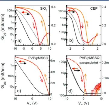
Fully printed transistors require not only optimization of processes for depositing the channel material but also selection of compatible materials for the dielectric as well as the source, drain, and gate electrodes.59 Selection of printable dielectrics com-patible with the channel material is particularly challenging. Figure 6illustrates the significant effect of the dielectric on device performance, comparing the transfer characteristics for three different dielectrics. Thermally grown SiO2, although not printable,
is commonly used to develop deposition processes, whereas cyanoethylated pullulan (CEP) and PVP-pMSSQ (a blend of poly(vinylphenol) and poly(methyl silsesquioxane)) are print-able polymer dielectrics. Transistors fabricated by inkjet printing of the SWCNT channel on SiO2provide an illustrative
example that exhibits a high on-state normalized conductance (∼0.4 mS/mm) and on/off ratio (>105). Switching to CEP, a
high dielectric constant polymer (κ ∼ 13), maintains the high on currents obtained on SiO2but at a reduced operating voltage of
<3 V. While use of this high-κ dielectric enables low-voltage
operation even for dielectric thicknesses that can be deposited reliably with printing methods (∼500 nm), driving these devices at even modest frequencies (>1 Hz) is found to significantly decrease the transconductance.60This behavior is a consequence of the slow polarization response of the dielectric, which leads to an enhancement of capacitance at low frequencies. Similar obser-vations have been reported for some elastomeric dielectrics.61 In selecting new dielectrics, particularly ones with high κ, testing the transistors’ frequency response is crucial to ensure that low-frequency polarization does not enhance transconductance in transfer characteristics. The high capacitance of CEP at low frequencies is reminiscent of the behavior of ion gels, consisting of ionic liquids incorporated into polymer networks. In these materials, very high capacitances (∼1−10 μF/cm2) arise from the
formation of a nanometer-thick electrical double layer, enabling high on currents at low operating voltages. Since their perfor-mance depends on ionic motion, these dielectrics exhibit signif-icant frequency and temperature dependence, but they have been shown to be useful in fabricating partially printed SWCNT-based ring oscillators operating at frequencies of >20 kHz at voltages of <3 V.62
For air-exposed SWCNT transistors, such as in gas sensors, hysteresis in gate voltage sweeps presents an important challenge and can be addressed with the use of hydrophobic polymer dielectrics. On CEP (water contact angle of ∼40−50°), the hysteresis is reduced to ∼1 V (Figure 6b). On PVP-pMSSQ, with contact angles of 80−100°, the hysteresis is essentially eliminated (Figure 6c). Although PFDD/SWCNTs do not adhere readily to hydrophobic dielectrics by soaking, a novel droplet electro-phoresis method was used to deposit dense SWCNT networks on these surfaces.63,64Elimination of hysteresis on hydrophobic dielectrics is consistent with the cause being a redox reaction involving oxygen and water.45 As can be seen in Figure 6d, deposition of an additional PVP-pMSSQ dielectric on top of the Figure 6.Normalized conductance as a function of gate voltage for bottom-gated SWCNT transistors on different dielectric materials: (a) on SiO2(L = 20 μm, W = 2000 μm, by inkjet printing); (b) on CEP
(L = 25 μm, W = 100 μm, by soaking); (c) on PVP-pMSSQ (L = 100 μm, W = 600 μm, by droplet electrophoresis); (d) same as (c) with an encapsulation layer of PVP-pMSSQ. VD= −1 V except in the case of
SWCNT channel shifts the threshold voltage to negative values so that the device is off at 0 V, which is important for digital logic applications. These results have also been observed in fully printed transistors using PVP-pMSSQ in the top-gated configuration.65
Realizing the full potential of printable electronics requires the development of high-throughput roll-to roll (R2R) processes to fabricate transistors on flexible substrates. While earlier demon-strations did not incorporate highly enriched sc-SWCNT dispersions,66,67we recently demonstrated the use of a hybrid process combining R2R gravure and inkjet printing to fabricate arrays of transistors.68As shown inFigure 7, this process leads to good electrical performance combined with excellent uniformity across rows of 20 transistors. Moreover, encapsulation acts positively to stabilize the transfer characteristics for up to 90 days while providing mobilities of >1 cm2V−1s−1. The variability of key device parameters, including threshold voltage and on current, is <10%, which is sufficient to drive e-paper display backplanes, an important practical step toward low-cost transistor arrays on flexible substrates. Demonstrations of truly fully printed transis-tors with mobility values of >1 cm2V−1s−1using commercially
relevant printing processes remain rare. Claims of fully printed devices may be made where steps not amenable to high-throughput printing have been used and immediately bring into question the viability from a low cost/commercial relevance standpoint.
■
SUMMARY AND FUTURE OUTLOOKRealizing some of the expected potential of sc-SWCNTs in electronic applications is within reach. Bulk enrichment of SWCNTs using conjugated polymers to produce high-purity semiconducting inks enables a variety of device demonstrations, from high-performance transistors to large-area, flexible, and stretchable R2R-printed transistors and sensors. Rapid optical-spectroscopy-based metrology techniques and relevant standards that keep pace with purity are necessary to support both process optimization and device production. Further research on SWCNT enrichment using novel dispersants, dopants, and unique solvent combinations should lead to better inks with application-specific attributes. Advantages realized with decom-posable dispersants are beginning to be exploited, with expected benefits in applications requiring pristine SWCNT surfaces,
such as sensors. An important opportunity exists with theory and modeling to provide a better description of enrichment mechanisms and support process optimization. As an integral part of a materials package, SWCNTs also need to find fit with other materials in a transistor. Mainly, proper selection of the gate dielectric and encapsulation layers is crucial, and few solutions are provided for hysteresis-free low-voltage operation. Improved strategies are needed to obtain stable n-channel TFTs that enable complimentary circuits with operating voltages < 1.5 V. While additive printing technologies continue to adapt to provide high uniformity, resolution, registration accuracy, etc. on large scales, transistors with mobilities of >20 cm2V−1s−1and low off
currents will provide a path to flexible OLED backplanes,69,70 while self-assembly and alignment techniques will enable mobilities of >100 cm2V−1s−1. As sc purity continues to improve toward
6N, bulk sc-SWCNTs are expected to continue on the path toward a viable Si replacement in high-end electronics, even if at first fulfilling the role of a complementary technology. The era of carbon-based electronics is finally in our sights, and high-purity
sc-SWCNTs are a key enabler to make it a reality.
■
AUTHOR INFORMATION Corresponding Authors *E-mail:[email protected]. *E-mail:[email protected]. ORCID Patrick R. L. Malenfant:0000-0001-5391-2300 NotesThe authors declare no competing financial interest.
Biographies
Jacques Lefebvreholds a Ph.D. from the University of Sherbrooke. He has over 15 years of exposure to various aspects of carbon nanotube electronics and photophysics.
Jianfu Dingreceived a Ph.D. from Nanjing University in 1992. He has over 25 years of experience in polymer science and is currently working on the development SWCNT enrichment.
Zhao Lireceived a Ph.D from the Chinese Academy of Sciences in 2000. He has 20 years of experience in polymer synthesis and application and Figure 7.Fully printed carbon nanotube transistors on a flexible substrate. (a) Overall view of a 20 × 20 array with source, drain, and gate electrodes visible. (b) Image of a single printed transistor. (c) SEM image of the nanotube network in the channel. (d) Transfer curves for 20 transistors along a row in the array. The inset shows a histogram of the threshold voltage.
Accounts of Chemical Research Article
DOI:10.1021/acs.accounts.7b00234
Acc. Chem. Res. 2017, 50, 2479−2486
is currently working on enrichment of SWCNTs and their application as sensors.
Paul Finniereceived a Ph.D. from the University of Ottawa in 1999. His current interests include the application of optical spectroscopy to the development of SWCNT technology.
Gregory Lopinskireceived a Ph.D. in 1993 from Brown University. He is currently working on characterization of solution-processable nanocarbon materials and devices.
Patrick R. L. Malenfantreceived a Ph.D. from UC Berkeley in 2000. He is currently a group leader working on the development of conductive inks and SWCNT-based electronics.
■
REFERENCES(1) Cao, Y.; Cong, S.; Cao, X.; Wu, F.; Liu, Q.; Amer, M. R.; Zhou, C. Review of Electronics Based on Single-Walled Carbon Nanotubes. Top Curr. Chem. (Z) 2017, 375, 75.
(2) Zhu, J.; Hersam, M. C. Assembly and electronic applications of colloidal nanomaterials. Adv. Mater. 2017, 29, 1603895.
(3) Islam, A. E.; Rogers, J. A.; Alam, M. A. Recent Progress in Obtaining Semiconducting Single-Walled Carbon Nanotubes for Transistor Applications. Adv. Mater. 2015, 27, 7908−7937.
(4) Nish, A.; Hwang, J.-Y.; Doig, J.; Nicholas, R. J. Highly Selective Dispersion of Single-walled Carbon Nanotubes Using Aromatic Polymers. Nat. Nanotechnol. 2007, 2, 640−646.
(5) Chen, F.; Wang, B.; Chen, Y.; Li, L.-J. Toward the Extraction of Single Species of Single-Walled Carbon Nanotubes Using Fluorene-Based Polymers. Nano Lett. 2007, 7, 3013−3017.
(6) Samanta, S. K.; Fritsch, M.; Scherf, U.; Gomulya, W. S.; Bisri, Z.; Loi, M. A. Conjugated Polymer-Assisted Dispersion of Single-Wall Carbon Nanotubes: The Power of Polymer Wrapping. Acc. Chem. Res. 2014, 47, 2446−2456.
(7) Lei, T.; Pochorovski, I.; Bao, Z. Separation of Semiconducting Carbon Nanotubes for Flexible and Stretchable Electronics Using Polymer Removable Method. Acc. Chem. Res. 2017, 50, 1096−1104.
(8) Zaumseil, J. Single-walled carbon nanotube networks for flexible and printed electronics. Semicond. Sci. Technol. 2015, 30, 074001−1−20. (9) Itkis, M. E.; Perea, D. E.; Jung, R.; Niyogi, S.; Haddon, R. C. Comparison of Analytical Techniques for Purity Evaluation of Single-Walled Carbon Nanotubes. J. Am. Chem. Soc. 2005, 127, 3439−3448.
(10) Jorio, A.; Dresselhaus, M.; Saito, R.; Dresselhaus, G. F. Raman Spectroscopy in Graphene Related Systems; Wiley-VCH: Weinheim, Germany, 2011.
(11) Fábián, G.; Kramberger, C.; Friedrich, A.; Simon, F.; Pichler, T. A broadband and high throughput single-monochromator Raman spectrometer: Application for single-wall carbon nanotubes. Rev. Sci. Instrum. 2011, 82, 023905.
(12) Finnie, P. Tunable filter Raman spectroscopy of purified semiconducting and metallic carbon nanotubes. Nano Res. 2016, 9, 2715−2728.
(13) Moura, L. G.; Moutinho, M. V. O.; Venezuela, P.; Fantini, C.; Righi, A.; Strano, M. S.; Pimenta, M. A. Raman excitation profile of the G band in single-chirality carbon nanotubes. Phys. Rev. B: Condens. Matter Mater. Phys. 2014, 89, 035402.
(14) Hároz, E. H.; Duque, J. G.; Barros, E. B.; Telg, H.; Simpson, J. R.; Hight Walker, A. R.; Khripin, C. Y.; Fagan, J. A.; Tu, X. M.; Zheng, M.; Kono, J.; Doorn, S. K. Asymmetric excitation profiles in the resonance Raman response of armchair carbon nanotubes. Phys. Rev. B: Condens. Matter Mater. Phys. 2015, 91, 205446.
(15) Finnie, P.; Ding, J.; Li, Z.; Kingston, C. T. Assessment of the Metallicity of Single-Wall Carbon Nanotube Ensembles at High Purities. J. Phys. Chem. C 2014, 118, 30127−30138.
(16) Li-Pook-Than, A.; Finnie, P. Observation of the metallic-type selective etching of single walled carbon nanotubes by real-time in situ two-laser Raman spectroscopy. Carbon 2015, 89, 232−241.
(17) Gontijo, R. N.; Sáfar, G. A. M.; Righi, A.; Jain, R. M.; Strano, M. S.; Fantini, C. Quantifying (n,m) species in single-wall carbon nanotubes
dispersions by combining Raman and optical absorption spectroscopies. Carbon 2017, 115, 681−687.
(18) Streit, J. K.; Bachilo, S. M.; Ghosh, S.; Lin, C.-W.; Weisman, R. B. Directly Measured Optical Absorption Cross Sections for Structure-Selected Single-Walled Carbon Nanotubes. Nano Lett. 2014, 14, 1530− 1536.
(19) Zhang, D.; Yang, J.; Yang, F.; Li, R.; Li, M.; Ji, D.; Li, Y. (n,m) Assignments and Quantification for Single-Walled Carbon Nanotubes on SiO2/Si Substrates by Resonant Raman Spectroscopy. Nanoscale
2015, 7, 10719−10727.
(20) Li, Z.; Ding, J.; Finnie, P.; Lefebvre, J.; Cheng, F.; Kingston, C. T.; Malenfant, P. R. L. Raman microscopy mapping for the purity assessment of chirality enriched carbon nanotube networks in thin film transistors. Nano Res. 2015, 8, 2179−2187.
(21) Li, Z.; Ding, J.; Lefebvre, J.; Malenfant, P. R. L. Surface effects on network formation of conjugated polymer wrapped semiconducting single walled carbon nanotubes and thin film transistor performance. Org. Electron. 2015, 26, 15−19.
(22) Bachilo, S. M.; Strano, M. S.; Kittrell, C.; Hauge, R. H.; Smalley, R. E.; Weisman, R. B. Structure-assigned optical spectra of single-walled carbon nanotubes. Science 2002, 298, 2361−2366.
(23) Luo, Z.; Papadimitrakopoulos, F.; Doorn, S. K. Bundling Effects on the Intensities of Second-order Raman Modes in Semiconducting Single-walled Carbon Nanotubes. Phys. Rev. B: Condens. Matter Mater. Phys. 2008, 77, 035421.
(24) Lefebvre, J.; Finnie, P. Photoluminescence and Förster Resonance Energy Transfer in Elemental Bundles of Single-Walled Carbon Nanotubes. J. Phys. Chem. C 2009, 113, 7536−7540.
(25) Ding, J.; Li, Z.; Lefebvre, J.; Cheng, F.; Dubey, G.; Zou, S.; Finnie, P.; Hrdina, A.; Scoles, L.; Lopinski, G. P.; Kingston, C. T.; Simard, B.; Malenfant, P. R. L. Enrichment of Large-diameter Semiconducting SWCNTs by Polyfluorene Extraction for High Network Density Thin Film Transistors. Nanoscale 2014, 6, 2328−2339.
(26) Gomulya, W.; Costanzo, G. D.; de Carvalho, E. J. F.; Bisri, S. Z.; Derenskyi, V.; Fritsch, M.; Fröhlich, N.; Allard, S.; Gordiichuk, P.; Herrmann, A.; Marrink, S. J.; dos Santos, M. C.; Scherf, U.; Loi, M. A. Semiconducting Single-Walled Carbon Nanotubes on Demand by Polymer Wrapping. Adv. Mater. 2013, 25, 2948−2956.
(27) Berton, N.; Lemasson, F.; Poschlad, A.; Meded, V.; Tristram, F.; Wenzel, W.; Hennrich, F.; Kappes, M. M.; Mayor, M. Selective Dispersion of Large-Diameter Semiconducting Single-Walled Carbon Nanotubes with Pyridine-Containing Copolymers. Small 2014, 10, 360−367.
(28) Lee, H. W.; Yoon, Y.; Park, S.; Oh, J. H.; Hong, S.; Liyanage, L. S.; Wang, H.; Morishita, S.; Patil, N.; Park, Y. J.; Park, J. J.; Spakowitz, A.; Galli, G.; Gygi, F.; Wong, P. H.-S.; Tok, J. B.-H.; Kim, J. M.; Bao, Z. Selective dispersion of high purity semiconducting single-walled carbon nanotubes with regioregular poly(3-alkylthiophene)s. Nat. Commun. 2011, 2, 541.
(29) Lemasson, F. A.; Strunk, T.; Gerstel, P.; Hennrich, F.; Lebedkin, S.; Barner-Kowollik, C.; Wenzel, W.; Kappes, M. M.; Mayor, M. Selective Dispersion of Single-Walled Carbon Nanotubes with Specific Chiral Indices by Poly(N-decyl-2,7-carbazole). J. Am. Chem. Soc. 2011, 133, 652−655.
(30) Fong, D.; Adronov, A. Recent Developments in the Selective Dispersion of Single-Walled Carbon Nanotubes Using Conjugated Polymers. Chem. Sci. 2017,DOI: 10.1039/C7SC02942J.
(31) Kim, K. S.; Cota-Sanchez, G.; Kingston, C. T.; Imris, M.; Simard, B.; Soucy, G. Large-Scale Production of Single Walled Carbon Nanotubes by Induction Thermal Plasma. J. Phys. D: Appl. Phys. 2007, 40, 2375−2387.
(32) Brady, G. J.; Way, A. J.; Safron, N. S.; Evensen, H. T.; Gopalan, P.; Arnold, M. S. Quasi-Ballistic Carbon Nanotube Array Transistors with Current Density Exceeding Si and GaAs. Sci. Adv. 2016, 2, e1601240.
(33) Jakubka, F.; Schießl, S. P.; Martin, S.; Englert, J. M.; Hauke, F.; Hirsch, A.; Zaumseil, J. ACS Macro Lett. 2012, 1, 815−819.
(34) Gerstel, P.; Klumpp, S.; Hennrich, F.; Poschlad, A.; Meded, V.; Blasco, E.; Wenzel, W.; Kappes, M. M.; Barner-Kowollik, C. ACS Macro Lett. 2014, 3, 10−15.
(35) Hwang, J.-Y.; Nish, A.; Doig, J.; Douven, S.; Chen, C.-W.; Chen, L.-C.; Nicholas, R. J. Polymer structure and solvent effects on the selective dispersion of single-walled carbon nanotubes. J. Am. Chem. Soc. 2008, 130, 3543−3553.
(36) Mistry, K. S.; Larsen, B. A.; Blackburn, J. L. High-Yield Dispersions of Large-Diameter Semiconducting Single-Walled Carbon Nanotubes with Tunable Narrow Chirality Distributions. ACS Nano 2013, 7, 2231−2239.
(37) Lei, T.; Lai, Y.-C.; Hong, G.; Wang, H.; Hayoz, P.; Weitz, R. T.; Chen, C.; Dai, H.; Bao, Z. Diketopyrrolopyrrole (DPP)-Based Donor− Acceptor Polymers for Selective Dispersion of Large-Diameter Semiconducting Carbon Nanotubes. Small 2015, 11, 2946−2954.
(38) Ding, J.; Li, Z.; Lefebvre, J.; Cheng, F.; Dunford, J. L.; Malenfant, P. R. L.; Humes, J.; Kroeger, J. A hybrid enrichment process combining conjugated polymer extraction and silica gel adsorption for high purity semiconducting single-walled carbon nanotubes (SWCNT). Nanoscale 2015, 7, 15741−15747.
(39) Fong, D.; Bodnaryk, W. J.; Rice, N. A.; Saem, S.; Moran-Mirabal, J. M.; Adronov, A. Influence of Polymer Electronics on Selective Dispersion of Single-Walled Carbon Nanotubes. Chem. - Eur. J. 2016, 22, 14413.
(40) Gui, H.; Streit, J. K.; Fagan, J. A.; Hight Walker, A. R.; Zhou, C.; Zheng, M. Redox Sorting of Carbon Nanotubes. Nano Lett. 2015, 15, 1642−1646.
(41) Khripin, C. Y.; Fagan, J. A.; Zheng, M. Spontaneous Partition of Carbon Nanotubes in Polymer-Modified Aqueous Phases. J. Am. Chem. Soc. 2013, 135, 6822−6825.
(42) Collins, P. G.; Bradley, K.; Ishigami, M.; Zettl, A. Extreme Oxygen Sensitivity of Electronic Properties of Carbon Nanotubes. Science 2000, 287, 1801−1804.
(43) O’Connell, M. J.; Eibergen, E. E.; Doorn, S. K. Chiral Selectivity in the Charge-Transfer Bleaching of Single-Walled Carbon Nanotube Spectra. Nat. Mater. 2005, 4, 412−418.
(44) Moonoosawmy, K. R.; Kruse, P. Cause and Consequence of Carbon Nanotube Doping in Water and Aqueous Media. J. Am. Chem. Soc. 2010, 132, 1572−1577.
(45) Aguirre, C. M.; Levesque, P. L.; Paillet, M.; Lapointe, F.; St-Antoine, B. C.; Desjardins, P.; Martel, R. The Role of the Oxygen/Water Redox Couple in Suppressing Electron Conduction in Field-Effect Transistors. Adv. Mater. 2009, 21, 3087−3091.
(46) Ding, J.; Li, Z.; Lefebvre, J.; Du, X.; Malenfant, P. R. L. Mechanistic Consideration of pH Effect on the Enrichment of Semiconducting SWCNTs by Conjugated Polymer Extraction. J. Phys. Chem. C 2016, 120, 21946−21954.
(47) Joo, Y.; Brady, G. J.; Shea, M. J.; Oviedo, M. B.; Kanimozhi, C.; Schmitt, S. K.; Wong, B. M.; Arnold, M. S.; Gopalan, P. Isolation of Pristine Electronics Grade Semiconducting Carbon Nanotubes by Switching the Rigidity of the Wrapping Polymer Backbone on Demand. ACS Nano 2015, 9, 10203−10213.
(48) Liang, S.; Zhao, Y.; Adronov, A. Selective and Reversible Noncovalent Functionalization of Single-Walled Carbon Nanotubes by a pH-Responsive Vinylogous Tetrathiafulvalene−Fluorene Copolymer. J. Am. Chem. Soc. 2014, 136, 970−977.
(49) Toshimitsu, F.; Nakashima, N. Semiconducting Single-Walled Carbon Nanotubes Sorting with a Removable Solubilizer Based on Dynamic Supramolecular Coordination Chemistry. Nat. Commun. 2014, 5, 5041.
(50) Toshimitsu, F.; Nakashima, N. Facile Isolation of Adsorbent-Free Long and Highly-Pure Chirality-Selected Semiconducting Single-Walled Carbon Nanotubes Using A Hydrogen-bonding Supramolecular Polymer. Sci. Rep. 2016, 5, 18066.
(51) Lei, T.; Chen, X.; Pitner, G.; Wong, H. S. P.; Bao, Z. Removable and Recyclable Conjugated Polymers for Highly Selective and High Yield Dispersion and Release of Low-Cost Carbon Nanotubes. J. Am. Chem. Soc. 2016, 138, 802−805.
(52) Pochorovski, I.; Wang, H.; Feldblyum, J. I.; Zhang, X.; Antaris, A. L.; Bao, Z. H-bonded Supramolecular Polymer for the Selective Dispersion and Subsequent Release of Large-Diameter Semiconducting Single-Walled Carbon Nanotubes. J. Am. Chem. Soc. 2015, 137, 4328−4331.
(53) Chortos, A.; Pochorovski, I.; Lin, P.; Pitner, G.; Yan, X.; Gao, T. Z.; To, J. W. F.; Lei, T.; Will, J. W.; Wong, H.-S. P.; Bao, Z. Universal Selective Dispersion of Semiconducting Carbon Nanotubes from Commercial Sources Using a Supramolecular Polymer. ACS Nano 2017, 11, 5660−5669.
(54) Joo, Y.; Brady, G. J.; Kanimozhi, C.; Ko, J.; Shea, M. J.; Strand, M. T.; Arnold, M. S.; Gopalan, P. Polymer Free Electronic Grade Aligned Semiconducting Carbon Nanotube Array. ACS Appl. Mater. Interfaces 2017, 9, 28859.
(55) Brady, G. J.; Way, A. J.; Safron, N. S.; Evensen, H. T.; Gopalan, P.; Arnold, M. S. Quasi-Ballistic Carbon Nanotube Array Transistors with Current Density Exceeding Si and GaAs. Sci. Adv. 2016, 2, e1601240.
(56) Sangwan, V. K.; Ortiz, R. P.; Alaboson, J. M. P.; Emery, J. D.; Bedzyk, M. J.; Lauhon, L. J.; Marks, T. J.; Hersam, M. C. Fundamental Performance Limits of Carbon Nanotube Thin-Film Transistors Achieved Using Hybrid Molecular Dielectrics. ACS Nano 2012, 6, 7480−7488.
(57) McMorrow, J. J.; Cress, C. D.; Gaviria Rojas, W. A.; Geier, M. L.; Marks, T. J.; Hersam, M. C. Radiation-Hard Complementary Integrated Circuits Based on Semiconducting Single-Walled Carbon Nanotubes. ACS Nano 2017, 11, 2992−3000.
(58) Yeom, C.; Chen, K.; Kiriya, D.; Yu, Z.; Cho, G.; Javey, A. Large-Area Compliant Tactile Sensors Using Printed Carbon Nanotube Active-Matrix Backplanes. Adv. Mater. 2015, 27, 1561−1566.
(59) Noh, J.; Jung, M.; Jung, Y.; Yeom, C.; Pyo, M.; Cho, G. Key Issues With Printed Flexible Thin Film Transistors and Their Application in Disposable RF Sensors. Proc. IEEE 2015, 103, 554−566.
(60) Lopinski, G.; Du, N.; Dubey, G.; Lefebvre, J.; Li, Z.; Zou, S.; Malenfant, P. R.L. Cyanoethylated Pullulan as a High-K Solution Processable Polymer Gate Dielectric for SWCNT TFTs. Org. Electron. 2017, 42, 329−336.
(61) Kong, D.; Pfattner, R.; Chortos, A.; Lu, C.; Hinckley, A. C.; Wang, C.; Lee, W. Y.; Chung, J. W.; Bao, Z. Capacitance Characterization of Elastomeric Dielectrics for Applications in Intrinsically Stretchable Thin Film Transistors. Adv. Funct. Mater. 2016, 26, 4680−4686.
(62) Ha, M.; Seo, J.-W. T.; Prabhumirashi, P. L.; Zhang, W.; Geier, M. L.; Renn, M. J.; Kim, C. H.; Hersam, M. C.; Frisbie, C. D. Aerosol Jet Printed, Low Voltage, Electrolyte Gated Carbon Nanotube Ring Oscillators with Sub-5 μs Stage Delays. Nano Lett. 2013, 13, 954−960. (63) Lefebvre, J.; Ding, J. Carbon Nanotube Thin Film Transistors by Droplet Electrophoresis. Mater. Today Commun. 2017, 10, 72−79.
(64) Lefebvre, J.; Ding, J.; Li, Z.; Cheng, F.; Du, N.; Malenfant, P. R. L. Hysteresis Free Carbon Nanotube Thin Film Transistors Comprising Hydrophobic Dielectrics. Appl. Phys. Lett. 2015, 107, 243301.
(65) Cao, C.; Andrews, J. B.; Franklin, A. D. Completely Printed, Flexible, Stable, and Hysteresis-Free Carbon Nanotube Thin-Film Transistors via Aerosol Jet Printing. Adv. Electron. Mater. 2017, 3, 1700057.
(66) Lee, W.; Koo, H.; Sun, J.; Noh, J.; Kwon, K.-S.; Yeom, C.; Choi, Y.; Chen, K.; Javey, A.; Cho, G. A Fully Roll-to-Roll Gravure-Printed Carbon Nanotube-Based Active Matrix for Multi-Touch Sensors. Sci. Rep. 2016, 5, 17707.
(67) Noh, J.; Jung, M.; Jung, K.; Lee, G.; Kim, J.; Lim, S.; Kim, D.; Choi, Y.; Kim, Y.; Subramanian, V.; Cho, G. Fully Gravure-Printed D Flip-Flop on Plastic Foils Using Single-Walled Carbon-Nanotube-Based TFTs. IEEE Electron Device Lett. 2011, 32, 638−640.
(68) Homenick, C. M.; James, R.; Lopinski, G. P.; Dunford, J. L.; Sun, J.; Park, H.; Jung, Y.; Cho, G.; Malenfant, P. R. L. Fully Printed and Encapsulated SWCNT-Based Thin Film Transistors via a Combination of R2R Gravure and Inkjet Printing. ACS Appl. Mater. Interfaces 2016, 8, 27900−27910.
(69) Chen, P.; Fu, Y.; Aminirad, R.; Wang, C.; Zhang, J.; Wang, K.; Galatsis, K.; Zhou, C. Fully Printed Separated Carbon Nanotube Thin Film Transistor Circuits and Its Application in Organic Light Emitting Diode Control. Nano Lett. 2011, 11, 5301−5308.
(70) Xu, W.; Zhao, J.; Qian, L.; Han, X.; Wu, L.; Wu, W.; Song, M.; Zhou, L.; Su, W.; Wang, C.; Nie, S.; Cui, Z. Sorting of large-diameter semiconducting carbon nanotube and printed flexible driving circuit for organic light emitting diode (OLED). Nanoscale 2014, 6, 1589−1595.
Accounts of Chemical Research Article
DOI:10.1021/acs.accounts.7b00234
Acc. Chem. Res. 2017, 50, 2479−2486