HAL Id: hal-01508981
https://hal.sorbonne-universite.fr/hal-01508981
Submitted on 12 Feb 2018HAL is a multi-disciplinary open access archive for the deposit and dissemination of sci-entific research documents, whether they are pub-lished or not. The documents may come from teaching and research institutions in France or abroad, or from public or private research centers.
L’archive ouverte pluridisciplinaire HAL, est destinée au dépôt et à la diffusion de documents scientifiques de niveau recherche, publiés ou non, émanant des établissements d’enseignement et de recherche français ou étrangers, des laboratoires publics ou privés.
In Depth Spatially Inhomogeneous Phase Transition in
Epitaxial MnAs Film on GaAs(001)
Christophe Gatel, Xiaoxiao Fu, Virginie Serin, M. Eddrief, Victor H. Etgens,
Bénédicte Warot-Fonrose
To cite this version:
Christophe Gatel, Xiaoxiao Fu, Virginie Serin, M. Eddrief, Victor H. Etgens, et al.. In Depth Spatially Inhomogeneous Phase Transition in Epitaxial MnAs Film on GaAs(001). Nano Letters, American Chemical Society, 2017, 17 (4), pp.2460-2466. �10.1021/acs.nanolett.7b00144�. �hal-01508981�
In depth spatially inhomogeneous phase transition in epitaxial MnAs film
on GaAs(001)
C. Gatel1*, X. Fu1, V. Serin1, M. Eddrief2, V. Etgens3 and B. Warot-Fonrose1*
1
CEMES CNRS-UPR 8011, Université de Toulouse, 31055 Toulouse, France
2
INSP CNRS-UMR 7588, Sorbonne Universités-UPMC 75252 Paris, France
3
LISV, Université Versailles St-Quentin, 78140 Vélizy, France
* Corresponding authors: gatel@cemes.fr
warot@cemes.fr
Keywords: Electron holography, in situ TEM, magnetic materials, phase transition, thin film, MnAs,
Abstract. Most studies on MnAs material in its bulk form have been focused on its temperature dependent structural phase transition accompanied by a magnetic one. Magnetostructural phase transition parameters in thin MnAs films grown on GaAs substrate present however some differences from the bulk behavior, and local studies become mandatory for a deeper understanding of the mechanisms involved within the transition. Up to now, only surface techniques have been carried on, while the transition is a three dimensional phenomenon. We therefore developed an original nanometer scale methodology using electron holography to investigate the phase transition in an epitaxial MnAs thin film on GaAs(001) from the cross-section view. Using quantitative magnetic maps recorded at the nanometer scale as function of the temperature, our work provides a direct in situ observation
of the inhomogeneous spatial distribution of the transition in the layer depth and brings new insights on the fundamental transition mechanisms.
Introduction. Epitaxial MnAs thin films on GaAs substrate have been attracting much interest for their potential applications in spintronic devices,1–3 especially for spin injection. A thorough understanding of their magnetic domain configurations is therefore crucial for developing efficient devices. MnAs presents a remarkable magnetostructural phase transition from the ferromagnetic (FM) hexagonal α phase (NiAs type symmetry, B81) to
non-ferromagnetic (N-FM) orthorhombic β phase (MnP type symmetry, B31) around 40°C with
temperature rising.4,5 Most interestingly, the parameters of this first order transition are different in MnAs thin films grown on GaAs substrate compared to bulk MnAs.5 The temperature range where α and β domains coexist broadens and varies with the film thickness, orientation and deposition conditions. The phase coexistence is explained by the constrained lateral size and constant mean lattice spacing in the MnAs layer:6,7 the thermal dilatation and crystalline transformation give rise to elastic strain that can be relaxed through the coexistence of α and β domains.
The investigation of the transition mechanisms has been proposed using many different methods studying the transition either from a purely structural point of view,5,7–9 or from the corresponding magnetic states.5,8,10,11 Local techniques as high resolution transmission electron microscopy (TEM) can hardly bring accurate structural information as the lattice parameter difference between the two phases is too small and the crystal domain boundaries do not exhibit any singular features.5,8 Local magnetic techniques have therefore been used, such as magnetic force microscopy (MFM),11–13 and X-ray magnetic circular dichroism photoemission electron microscopy (XMCD-PEEM).10,14 Viewed from the film surface plane, the FM α-MnAs and N-FM β-MnAs phases coexist in a form of self-aligned array of stripes between around 20 and 50°C,7,15 and the width of α-MnAs stripes is continuously tunable by varying the temperature.10,11,14
The knowledge of the in-plane magnetic configuration is not sufficient to offer a full understanding of the structural local transition mechanisms in MnAs thin films for future applications. The cross-section in-depth information with quantitative values of the magnetization at the nanometer scale is mandatory for a deeper analysis of the transition. So far, simulations have been performed on the cross-section views of magnetic configurations, or three-dimensional configurations, as complements to the in-plane experimental findings.13,16,17 An experimental MFM study of the MnAs/GaAs sample cleaved in the
cross-section configuration has been once reported, showing the coexistence of α and β domains. The α submicron-wide domains have a constant magnetization along the easy axis direction from the top surface to the interface with the substrate.18 However, this conclusion is open to doubt: the probed area may be altered by the surface effects and consequently the measured properties will not correspond to the ones of the inner layer. Possible effects of surface and interface as well as inevitable defects on the magnetization of the film19–21 may also not be resolved due to the spatial resolution limited to a few tens of nanometers with the MFM technique.
We consequently chose to apply off-axis electron holography (EH), which combines a high spatial resolution and high sensitivity toward local magnetic induction but also the capability of quantifying the magnetization in the inner part of samples.22–26 We have thus in
situ investigated the magnetostructural phase transition in a cross-sectional 180 nm thick
MnAs film by studying the evolution of its magnetic configurations. Our results provide a direct and quantified observation of the inhomogeneous spatial distribution of the transition in the layer depth, and bring new insights on the transition mechanisms.
Experiments. A 180 nm MnAs layer was grown using solid-source Molecular Beam Epitaxy (MBE) on a semi-insulating GaAs(001) substrate.8,15 The epitaxial relationship of this α-MnAs thin film and the GaAs (001) substrate as well as the α and β crystallographic structures have been clearly identified in a previous TEM study.27 A cross-section lamella was prepared by Focused Ion beam (FIB) to ensure a uniform thickness crossed by the electron beam for the EH experiment. To avoid ion beam damages on the MnAs layer top surface, a 400nm thick Pt was deposited on it before any thinning process. The lamella was then thinned down to 80 nm along the MnAs[0001] axis. The MnAs easy axis10,28 was therefore kept in the lamella plane. The details of the conventional TEM images and diffraction pattern are summarized in Supporting Information (SI). For the sake of clarity, the interfaces of MnAs with GaAs and Pt will be respectively named “interface” and “surface” in the following text.
EH experiments were performed on a 300kV Hitachi HF3300C TEM equipped with two electron biprism stages. The TEM was operated in a specific corrected Lorentz mode, allowing a spatial resolution down to 0.5 nm in a magnetic field-free sample environment. A Gatan HC3500 single-tilt sample-holder was used to control the temperature of the lamella inside the TEM. The cross-section lamella was in situ magnetically saturated along the easy
axis , and then slightly tilted away from the zone axis to avoid dynamical diffraction effects before being observed at the remnant state. Two different areas, namely area A and B, in the lamella were investigated (see SI). For area A, holograms were acquired with a temperature step of 2°C in both heating and cooling processes between 23°C (RT) and 50°C. For area B, the hologram acquisition was performed down to 1°C step, but only in the cooling process and repeated twice. All the holograms were acquired with an interference fringe spacing set to 1.3 nm after temperature stabilization to perform a static study of the transition. In total, a little less than 1000 holograms were recorded throughout the experiment. Magnetic phase shift maps were extracted from holograms by applying a numerical cosine mask on one of the side-band after calculating the fast Fourier transform (see SI). The mask size has been chosen to get the best compromise between the final spatial resolution (here equal to 3 nm) and the signal over noise ratio. We checked between the beginning and the end of the full EH experiment that the MnAs layer has not been modified by the irradiation of the electron beam by comparing the amplitude images. We also compared the magnetic phase images obtained at the same temperatures after several heating/cooling cycles. Finally, three sets of temperature-dependent magnetic phase shift maps of the cross-section MnAs film were obtained.
The full quantification procedure of the magnetic induction from the phase shift maps is detailed in SI. In the following, x and y axis correspond to the and
[ ]
1100 MnAs directions respectively. z axis is thus parallel to the direction (hard magnetic axis) and to the electron beam path. Using the Aharonov-Bohm equations,29,30 the x component of the magnetic induction, noted Bx, can be obtained from a defined area within the MnAs layer byanalyzing the mean slope of the magnetic phase shift along the y direction:
(eq. 1)
e being the elementary charge, and the reduced Planck constant. Measuring the lamella width w crossed by the electron beam and assuming that the magnetization is equivalent to the induction inside the MnAs layer, it is then possible to attain the x component of the mean magnetization, noted µOMx: (eq. 2)
[ ]
1120[
0001]
[ ]
1120[
0001]
M φ(
)
( )
y y x e dz z y x B M x ∂ ∂ =∫
, , η φ , η(
)
w dz z y x B Mx x∫
= , , 0 µRepeating this analysis as a function of the applied temperature T, the is plotted on a localized area of the field of view. The resulting graph is therefore strictly equivalent to the classical M(T) curve obtained by magnetometry (Vibrating sample magnetometry,…).
Results. Figure 1 presents the amplitude image and the magnetic phase images of the area A for two temperatures, 23°C and 50°C.
Figure 1. (a) Amplitude image of area A (2200 nm x 380 nm); (b) Magnetic phase shift map of area A obtained at 23°C and (c) at 50°C. Enlarged sub-area “1” (150x300 nm²) extracted from (b) for (d) amplitude image, (e) magnetic phase shift at 23°C, (f) magnetic phase shift at 23°C without phase jumps (unwrapping process), of the amplitude image, g) magnetic phase shift at 50°C; (h) Magnetic phase shift profiles along the y direction at 23°C and 50°C, averaged over 150 nm along the x direction in the sub-area “1”; (i) Evolution of the x component of the magnetization as a function of temperature T for both the heating (red) and cooling (blue) processes, measured in the sub-areas “1” and “2” shown in (b).
( )
T f Mx =The MnAs layer presents some contrast variations in the amplitude image that are attributed to the presence of defects as observed in previous works.5,31,32 Phase images of Figure 1(b-c) display the magnetic phase shift as color contrasts at extreme temperatures. At RT (23°C), the FM state corresponding to the α-MnAs phase is clearly identified by the appearance of a variation of the phase shift inside the MnAs layer. The difference between phase values in Pt and GaAs is linked to the presence of a magnetic induction within the MnAs layer. The projected induction in the xy plane being parallel to the isophase lines, i.e. to the color stripes and phase jumps between –π and +π, the induction direction is along the direction (x axis) as denoted by the white arrow. Quantitative information is then extracted using the phase shift profile from the rectangular sub-area noted 1 and displayed in Figure 1(h) after removing phase jumps. In this profile, the plateau in the Pt and GaAs sections indicates no induction outside the MnAs layer, while the linear variation in the MnAs section proves that the induction spreads homogeneously along the y axis inside the MnAs layer. As detailed in SI, 4 nm thick layers of MnAs close to the bottom interface and the top surface were affected by artifacts due to data processing and consequently excluded from the analysis. The phase shift profile is the same on the whole field of view, indicating that the MnAs layer at 23°C presents also an homogeneous magnetization along the x axis without effect from lamella preparation that could have broken the FM order. The constant slope of 0.086±0.006 rad.nm-1 in the MnAs layer gives an integrated induction of 57±4 T.nm (eq. 1) distributed homogeneously in the film thickness. With w measured to 80±5nm during the lamella preparation, the mean magnetization µ0Mx is equal to 0.7±0.1 T (557±80 emu.cm-3).
This value is in agreement with others saturation magnetization values obtained at the FM state in the literature.5,33,34 At 50°C (Figure 1(c)), no phase shift variation is observed, the phase values are the same between Pt and GaAs substrate. Therefore the constant phase term (set at 0) in the phase profile obtained on the same sub-area 1 of Figure 1(h) corresponds to a zero magnetization in the xy plane. This evidences that the FM α-MnAs detected at RT has been completely transformed to N-FM β-MnAs at 50°C.
Through intermediate magnetic phase shift maps obtained every 2°C in both cooling and heating process, complete loops for 23°C < T <50°C were calculated by repeating the previous analysis on the sub-areas 1 and 2 (Figure 1(i)). Error bars are absent for clarity but they are between ±0.02 and ±0.1 T at each point. The sub-area 2 has the same width as sub-area 1 but is located in a different position along the x axis as denoted in Figure 1(b). The loops are similar for both sub-areas: the magnetization is decreasing during heating
[ ]
1120( )
T f Mx = 0µ
and the trend is inverse during cooling. The heating curve and the cooling one are almost superimposed with a slight loop opening of 2°C, demonstrating a local quasi-reversible phase transition. However the loops between sub-areas are shifted by approximately 4°C indicating a non-homogeneous transition along the x axis. Defining the transition temperature TT as the
one at which the magnetization is the mid-value of those at RT and 50°C (0.35 T), the heating and cooling curves have very close TT values of 41±2°C and 37±2°C for sub-areas 1 and 2
respectively. These values are in agreement with previous works.5
The intermediate magnetic phase shift maps obtained between 23°C and 50°C were analyzed to study the inhomogeneity of the magnetostructural transition along the x axis, but also the transition process in the depth of the MnAs layer (y axis). Figure 2 presents some magnetic phase images recorded during the heating and cooling process of area A. It is worth noticing that the incident electron beam is parallel to the MnAs magnetic hard axis, which is parallel to the length direction of α and β stripes and perpendicular to the
magnetic easy axis,28 so that the cross sections of both α and β stripes are visible. As already illustrated in Figure 1(b), FM contrasts corresponding to α domains present phase shift variations inside the MnAs layer giving isophase lines parallel to the magnetic induction while β domains correspond to area without such lines, i.e. where there is no magnetization. On the contrary to the extreme case of pure N-FM state of Figure 1(c), phase variations can still be visible in some β domains in Figure 2 during the transition, especially at low temperatures. The corresponding magnetic induction in the positions of β domains come from the leakage field between two adjacent FM α domains. In addition, as the measured phase shift corresponds to a two dimensional projection of a three dimensional field, a non-zero value of the phase shift can be obtained if α and β domains coexists in the width of the lamella. Even so, the presence of β domains can be identified by the leakage field around, and a decrease of the phase shift slope corresponding to a reduced magnetization compared to the adjacent α ones. At higher temperatures, the α domains are more separated with weaker intercoupling, and the β domains present more obvious leakage field and less visible color variation. The results of the phase identification are displayed on the different maps of Figure 2 in the GaAs part for better clarity. The appearance of a slight phase variation in Pt and GaAs at the right part of the phase images in the ferromagnetic state is due to a magnetic leak field related to the thin lamella geometry (See SI for details). From those maps we perceive that the β domains nucleate either from the surface/interface or from localized zones in the core of the layer, and expand both in x and y directions during heating.
[
0001]
Figure 2. Magnetic phase shift maps of the area A at various temperatures in the heating (left hand side column) and cooling (right hand side column) processes. In those images presenting the phase coexistence, the MnAs layer is between horitonzal dashed line at left of each image. Positions and width of the α and β domains are denoted in the GaAs layer (black and white legends are for contrast purpose only). Two different types of α domains are noted. The bold white or black arrows in the MnAs layer indicate the direction of the local magnetic induction.
A very interesting point is the identification of two different types of α domains if our analysis is focused on the phase images obtained between 44°C and 48°C. The first one, referred as “Type-I”, presents a magnetization along the magnetic easy axis. Type-I domains initially appear in the core of the MnAs layer at approximatively 75 nm from the interface with GaAs, and then expand preferentially along the x direction during cooling.
These Type-I domains correspond to the α-MnAs stripes previously observed by the surface-based methods.5,10,11 The other type, denoted as “Type-II”, is smaller and shows a magnetization direction along the growth axis i.e. the
[ ]
1100 . Remarkably, α Type-II domains always appear close to the GaAs interface and experience no spatial expansion. During the cooling process and the spatial extension of α Type-I domains, the α Type-II domains become less visible but still coexist with α Type-I domains down to RT.Comparing the heating and cooling series, the evolution is perfectly reversible. It is worth noting that phase images are very similar between both series for a neighbouring temperature. The only difference between cooling and heating series occurs down to 42°C for one α Type-I domain in the cooling series: its magnetization, opposite to the one of the adjacent α Type-I domains (black and white arrows), experiences a 180 degrees rotation when the increasing dipolar energy with the adjacent α Type-I domains becomes too large. Nevertheless, following the locations of α and β domains, it is easy to find that the positions where the phase transition initially occurs are not random but fixed. The areas in MnAs where β domains appear first during the heating process correspond to areas where the β domains disappear last during cooling. The same remark is still valuable for α domains: the first α domains appearing during the cooling process are localized in the same areas and present the same features (Type I or II) than the last α domains disappearing during heating. The fixed positions of α and β domains demonstrate an obvious correlation between structural inhomogeneities and preferential nucleation sites of α and β domains.
In a structure-dependent magnetic phase transition, the defects are likely to play important roles. For the studied sample, some defects, e.g. the grain boundaries and possibly edge dislocations,31 are visible in the amplitude image of Figure 1 (a), but it is difficult to establish a clear correspondance between contrasts in the amplitude image and the appearance of magnetic domains in the phase images. The α Type II domains located at the interface and presenting a local change of the magnetocristalline anisotropy are certainly favored by the defects. The temperature hysterisis of magnetization revealed by SQUID in literature31 was experimentally verified to be related with the crystal defects. Moreover, an array of misfit dislocations was observed in high resolution TEM images when the incident beam is parallel to MnAs[0001]//GaAs[1-10].5,27,34 It relieves the strain introduced by the 7% misfit between the MnAs and GaAs lattice along the MnAs axis.34 As the distance between these misfit dislocations is generally about 4.5 nm34 while the interval spacing of β domains is
hundreds of nanometers, a direct correlation between the misfit dislocations and the locations of domain nucleation could not be supported yet, but worth to be explored.
It is interesting to note that α Type II domains can interact with magnetic domain walls as seen on the phase images in Figure 2 during cooling when the α Type-I domain in the centre of the image presents an opposite magnetization with the others (see phase images at 42°C, 44°C and 46°C of the cooling series). This effect is clearly highlighted by the EH experiments performed on the other area named B. Figure 3 displays the amplitude and magnetic phase images for one of the cooling series recorded on the area B. Two repeated experiments on this area provided exactly the same locations of α and β domains, confirming that the magnetic phase transition of MnAs thin films is closely dependent on the crystal structure. At 50°C, the constant phase shift indicates no magnetization is present and therefore the whole MnAs layer is in the β phase. The two types of α domains appears at 45°C with the same characteristics previously described. A large β domain remains in the centre of the area B with a reducing lateral extension when decreasing the temperature, while the smallest β domains disappear progressivly with the lateral extension of the α Type-I domains. From 43°C, we clearly observe α Type-I domains with opposite magnetizations between the central part of the images and both extremities (horizontal white arrows). As a consequence, two 180-degree domain walls appear, as spotted by vertical arrows in the Pt part in the phase image recorded at 41°C. The left one is for instance located at about 150 nm on the left of a α Type-II domains. At 40°C, the domain walls shift towards the specific positions of α Type-II domains and are finally stabilized in these positions (vertical arrows in the Pt part). This leads to the conclusion that the α Type-II domains probably due to structural defects help to stabilize the magnetic walls of adjacent α Type-I domains if their respective magnetizations remain unchanged. They play a definite role on the final magnetic configuration.
Figure 3. On the top is the amplitude image of the area B (2900 nm x 380 nm); below are displayed the magnetic phase shift maps of the same area at various temperatures in the cooling process. The MnAs layer is between horitonzal dashed line at left of each image. Positions and width of the α and β domains are denoted. The horizontal white arrows indicate the magnetic induction directions of
α
Type- I domains in the MnAs layer.In addition to the defect influence, Figures 2 and 3 also demonstrate significant surface and interface effects. The magnetic contrasts corresponding to α Type-I domains always initially appear in a well defined position at about 75 nm from the interface as previously mentioned, grow laterally along the x direction, and then gradually expand in the y direction towards the surface and interface. A quantitative analysis of the transition along the
y axis is thus of interest. We performed this analysis on the sub-area enclosed by the white
rectangle displayed in Figure 3 on the 50°C phase image. This sub-area corresponds to the entire thickness of the MnAs layer with a lateral extension of 300 nm along the x direction. A rectangular mask with dimensions x = 300 nm and y = 9 nm was used to extract a portion of the sub-area and to calculate the corresponding curve
µ
0Mx = f( )
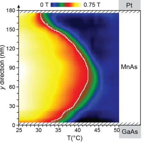
T . This mask was shifted by2 nm along the y direction from the interface with GaAs to the surface. A three-dimensional map is then depicted in Figure 4 where both the temperature and thickness dependences of magnetization are mapped. The white curve representing the transition temperature TT as a
function of the position y within the layer clearly displays how the phase transition is inhomogeneous along the growth direction. The transition temperatures in the areas closer to surface and interface are slightly different by 2°C. In the areas further away from the surface and interface, the transition temperatures are obviously higher. The maximum difference reaches 11°C at 75 nm from the interface corresponding to the position where the α Type-I domains appear. Interestingly, the temperature range of the transition (width between yellow and blue parts) decreases strongly for the area close to the surface.
Figure 4. Map of the magnetization as a function of the temperature and the position in the layer depth. It corresponds to the evolution of the transition in the film thickness during cooling for the sub-area enclosed by a white rectangle displayed in Figure 3 on the 50°C magnetic phase image. The color scale corresponds to the magnitude of the magnetization and the transition temperature is displayed by the white profile corresponding to a magnetization of 0.35 T.
A previous study35 demonstrated a decrease of TT when increasing the pressure
Indeed the β phase cell volume being smaller than the α phase cell volume, the α to β phase transition is favored for high pressure. In a similar way, TT is lowered for strained regions if a
compressive epitaxial strain is applied on MnAs thin films.33,36,37 The epitaxial strain generated from the interface and decreasing when going to the surface37,38 explains the low values of TT for area close to the interface followed by a gradual increase. However, if this
effect was the only one, TT should increase on the whole thickness of the layer. The analysis
of the Figure 4 however indicates that the temperature reaches a maximum at 75 nm from the GaAs interface before diminishing towards the surface. An effect of the surface has thus to be taken into account. Assuming that the interface with Pt deposited by FIB for the lamella preparation is equivalent to a free surface, TT is lowered as the crystal is free to make its
volume changes. This effect observed in nanoparticles and in thin films38,39 would also explain the decrease of the temperature range for the transition as revealed in Figure 4. However this assumption needs to be discussed as Pt could exert strain on the MnAs/Pt interface. In this case, the strain would be a compressive strain for generating a decrease of TT
from the surface. Nevertheless the free surface effect appears certainly on the surfaces on each side of the TEM lamella created by the FIB preparation and parallel to the image plane.
These effects of interface and surface have been highlighted and discussed from Figure 4 which was calculated from a homogeneous area along the x axis for the transition. However, inhomogeneities of TT along the direction were evidenced on Figures 1, 2
and 3. Local variation of the strain due to defects or others structural inhomogeneities could modulate the transition temperature along the x axis and would explain why α and β phases preferentially appear or disappear in different regions. It is nevertheless interesting to underline that for a “homogeneous” region parallel to the direction, the transition is inhomogeneous along the growth direction because of the surface and interface effects.
Successive schemes of the MnAs temperature-dependent magnetostructural transition have therefore been determined by EH. The transition being reversible, we can use the cooling process (N-FM state to FM state) as an example: two types of α domains nucleate, Type-I at about 75 nm from the interface and Type-II at the interface with an unnormal magnetic anisotropy. Type-I domains quickly extend laterally (x direction) while Type-II domains can help for stabilizing the magnetic walls of adjacent α Type-I domains. The transition is almost achieved in the inner part when the induction starts to increase in areas close to surface and interface. The surface and interface do not seem to show the appearance
[ ]
1120of nuclei (apart α Type-II domains at the interface which do not experience lateral extension) but a more homogeneous and difficult transition which finish the complete transition of the MnAs layer.
Conclusion. An in situ observation of the magnetostructural phase transition in a MnAs thin film is presented on a cross-section view using electron holography (EH). From a series of high-resolution temperature-dependent magnetic phase shift maps, the spatially inhomogeneous phase transition along the MnAs magnetic easy axis as well as the
[ ]
1100 growth direction is unambiguously evidenced and quantitatively analyzed. Our original EH nanometer scale methodology highlights also the existence of two type of α domains.During the β to α cooling phase transition, magnetic local α-Type I FM domains appear within the N-FM β phase close to the middle of the film thickness (about 75 nm from the interface with the substrate) before experiencing a lateral extension. We demonstrated that the β to α transition is favoured for areas close to surface and interface and this induces a 10°C amplitude of the transition temperature within the layer. Additionally, the presence of crystal defects and/or constraints in both interfaces delays the magnetic arrangement and modulates the transition along the axis of MnAs film. More singularly α Type-II domains localized at the bottom interface with a different magnetic anisotropy play an important role in stabilizing the magnetic walls of adjacent α Type-I domains. The interplay between structural inhomogeneities, strain, and preferential nucleation sites of α and β domains is thus demonstrated. Our experiment provides new information on the phase transition of MnAs thin film, which may enhance the fundamental understanding of this material and benefit its real application in spintronic devices. The three-dimensional mapping of the temperature-dependent magnetization and strains as well as the investigation of atomic scale mechanism in the transition process will be of high values to further reveal the ultimate principle of spatially inhomogeneous phase transition in MnAs/GaAs.
Acknowledgement.
The authors acknowledge the French National Research Agency under the "Investissement d'Avenir" program reference No. ANR-10-EQPX-38-01" the "Conseil Regional Midi-Pyrénées" and the European FEDER for financial support within the CPER program. This work was supported by the French national project EMMA (ANR12 BS10 013 01).
[ ]
1120Supporting information:
Contents: Description of the sample and thin lamella preparation, transmission electron microscope and heating-cooling sample holder, methods and hologram series, principle of electron holography, data treatment.
Note: The authors declare no competing financial interest.
Reference
(1) Ramsteiner, M.; Hao, H. Y.; Kawarahazuka, A.; Zhu, H. J.; Kästner, M.; Hey, R.; Däweritz, L.; Grahn, H. T.; Ploog, K. H. Phys. Rev. B Solid State 2002, 66, 081304(R). (2) Garcia, V.; Jaffrès, H.; George, J.-M.; Marangolo, M.; Eddrief, M.; Etgens, V. H. Phys.
Rev. Lett. 2006, 97, 246802.
(3) Pampuch, C.; Das, A. K.; Ney, A.; Däweritz, L.; Koch, R.; Ploog, K. H. Phys. Rev. Lett. 2003, 91, 147203.
(4) Okamoto, H. Bull. Alloy Phase Diagr. 1989, 10, 549–554. (5) Däweritz, L. Rep. Prog. Phys. 2006, 69, 2581.
(6) Das, A. K.; Pampuch, C.; Ney, A.; Hesjedal, T.; Däweritz, L.; Koch, R.; Ploog, K. H.
Phys. Rev. Lett. 2003, 91, 087203.
(7) Kaganer, V. M.; Jenichen, B.; Schippan, F.; Braun, W.; Däweritz, L.; Ploog, K. H.
Phys. Rev. B 2002, 66, 045305.
(8) Fu, X.; Warot-Fonrose, B.; Arras, R.; Demaille, D.; Eddrief, M.; Etgens, V.; Serin, V.
Appl. Phys. Lett. 2015, 107, 062402.
(9) Mohanty, J.; Hesjedal, T.; Plake, T.; Kästner, M.; Däweritz, L.; Ploog, K. H. Appl.
Phys. A 2003, 77, 739–742.
(10) Engel-Herbert, R.; Locatelli, A.; Cherifi, S.; Schaadt, D. M.; Mohanty, J.; Ploog, K. H.; Bauer, E.; Belkhou, R.; Heun, S.; Pavlovska, A.; Leo, T.; Hesjedal, T. Appl. Phys. A 2006, 84, 231–236.
(11) Kim, J.; Akinaga, H.; Kim, J. Appl. Phys. Lett. 2011, 98, 102511.
(12) Manago, T.; Kuramochi, H.; Akinaga, H. Surf. Sci. 2006, 600, 4155–4159. (13) Engel-Herbert, R.; Hesjedal, T.; Schaadt, D. M. Phys. Rev. B 2007, 75, 094430. (14) Engel-Herbert, R.; Schaadt, D. M.; Cherifi, S.; Bauer, E.; Belkhou, R.; Locatelli, A.;
Heun, S.; Pavlovska, A.; Mohanty, J.; Ploog, K. H.; Hesjedal, T. J. Magn. Magn. Mater. 2006, 305, 457–463.
(15) Breitwieser, R.; Vidal, F.; Graff, I. L.; Marangolo, M.; Eddrief, M.; Boulliard, J.-C.; Etgens, V. H. Phys. Rev. B 2009, 80, 045403.
(16) Engel-Herbert, R.; Hesjedal, T.; Schaadt, D. M. J. Appl. Phys. 2007, 101, 09K103. (17) Engel-Herbert, R.; Hesjedal, T.; Mohanty, J.; Schaadt, D. M.; Ploog, K. H. Phys. Rev.
(18) Salles, B. R.; Marangolo, M.; David, C.; Girard, J. C. Appl. Phys. Lett. 2010, 96, 052510.
(19) Li, Y. L.; Hu, S. Y.; Liu, Z. K.; Chen, L. Q. Appl. Phys. Lett. 2001, 78, 3878–3880. (20) Bratkovsky, A. M.; Levanyuk, A. P. Phys. Rev. Lett. 2005, 94, 107601.
(21) Hong, N. H.; Sakai, J.; Poirot, N.; Brizé, V. Phys. Rev. B 2006, 73, 132404. (22) McCartney, M. R.; Smith, D. J. Annu. Rev. Mater. Res. 2007, 37, 729–767. (23) Gatel, C.; Bonilla, F. J.; Meffre, A.; Snoeck, E.; Warot-Fonrose, B.; Chaudret, B.;
Lacroix, L.-M.; Blon, T. Nano Lett. 2015, 15, 6952–6957.
(24) Reyes, D.; Biziere, N.; Warot-Fonrose, B.; Wade, T.; Gatel, C. Nano Lett. 2016, 16, 1230–1236.
(25) Harrison, R. J.; Dunin-Borkowski, R. E.; Putnis, A. Proc. Natl. Acad. Sci. 2002, 99, 16556–16561.
(26) Masseboeuf, A.; Marty, A.; Bayle-Guillemaud, P.; Gatel, C.; Snoeck, E. Nanoletters 2009, 9, 2803–2806.
(27) Fu, X.; Warot-Fonrose, B.; Arras, R.; Seine, G.; Demaille, D.; Eddrief, M.; Etgens, V.; Serin, V. Phys. Rev. B 2016, 93, 104410.
(28) Ryu, K.-S.; Kim, J.; Lee, Y.; Akinaga, H.; Manago, T.; Viswan, R.; Shin, S.-C. Appl.
Phys. Lett. 2006, 89, 232506.
(29) Aharonov, Y.; Bohm, D. Phys. Rev. 1959, 115, 485–491. (30) Aharonov, Y.; Bohm, D. Phys. Rev. 1961, 123, 1511–1524.
(31) Däweritz, L.; Kästner, M.; Hesjedal, T.; Plake, T.; Jenichen, B.; Ploog, K. H. J. Cryst.
Growth 2003, 251, 297–302.
(32) Trampert, A.; Schippan, F.; Däweritz, L.; Ploog, K. H. Appl. Phys. Lett. 2001, 78, 2461–2463.
(33) Däweritz, L.; Herrmann, C.; Mohanty, J.; Hesjedal, T.; Ploog, K. H.; Bauer, E.; Locatelli, A.; Cherifi, S.; Belkhou, R.; Pavlovska, A.; Heun, S. J. Vac. Sci. Technol. B 2005, 23, 1759–1768.
(34) Ploog, K. H.; Däweritz, L.; Engel-Herbert, R.; Hesjedal, T. Phys. Status Solidi A 2006,
203, 3574–3580.
(35) Menyuk, N.; Kafalas, J. A.; Dwight, K.; Goodenough, J. B. Phys. Rev. 1969, 177, 942– 951.
(36) Xu, P.; Lu, J.; Chen, L.; Yan, S.; Meng, H.; Pan, G.; Zhao, J. Nanoscale Res. Lett. 2011,
6, 125.
(37) Garcia, V.; Sidis, Y.; Marangolo, M.; Vidal, F.; Eddrief, M.; Bourges, P.; Maccherozzi, F.; Ott, F.; Panaccione, G.; Etgens, V. H. Phys. Rev. Lett. 2007, 99, 117205.
(38) Iikawa, F.; Santos, P. V.; Kästner, M.; Schippan, F.; Däweritz, L. Phys. Rev. B 2002, 65, 205328.
(39) Tian, P.; Zhang, Y.; Senevirathne, K.; Brock, S. L.; Dixit, A.; Lawes, G.; Billinge, S. J. L. ACS Nano 2011, 5, 2970–2978.