HAL Id: hal-03026188
https://hal.archives-ouvertes.fr/hal-03026188
Submitted on 26 Nov 2020HAL is a multi-disciplinary open access archive for the deposit and dissemination of sci-entific research documents, whether they are pub-lished or not. The documents may come from teaching and research institutions in France or abroad, or from public or private research centers.
L’archive ouverte pluridisciplinaire HAL, est destinée au dépôt et à la diffusion de documents scientifiques de niveau recherche, publiés ou non, émanant des établissements d’enseignement et de recherche français ou étrangers, des laboratoires publics ou privés.
Measurement of the Spin-Forbidden Dark Excitons in
MoS2 and MoSe2 monolayers
Cédric Robert, B. Han, P. Kapuscinski, A. Delhomme, Clément Faugeras,
Thierry Amand, M. R. Molas, M. Bartos, K. Watanabe, T. Taniguchi, et al.
To cite this version:
Cédric Robert, B. Han, P. Kapuscinski, A. Delhomme, Clément Faugeras, et al.. Measurement of the Spin-Forbidden Dark Excitons in MoS2 and MoSe2 monolayers. Nature Communications, Nature Publishing Group, 2020, 11, pp.4037. �10.1038/s41467-020-17608-4�. �hal-03026188�
Measurement of the Spin-Forbidden Dark Excitons in MoS
2and MoSe
2monolayers
C. Robert1*†, B. Han1*†, P. Kapuscinski2,3†, A. Delhomme2,C. Faugeras2*, T. Amand1, M.R. Molas4, M. Bartos2,5, K. Watanabe6, T. Taniguchi6, B. Urbaszek1, M. Potemski2,4 & X. Marie11University of Toulouse, INSA-CNRS-UPS, LPCNO, 135 Av. Rangueil, 31077 Toulouse, France
2Laboratoire National des Champs Magnétiques Intenses, CNRS-UGA-UPS-INSA-EMFL, 38042 Grenoble,
France
Institute of Experimental Physics, Faculty of Physics, University of Warsaw, ul. Pasteura 5, 02-093 Warsaw, Poland
3 Wrocław University of Science and Technology, 50-370 Wrocław, Poland
4Institute of Experimental Physics, Faculty of Physics, University of Warsaw, 02-093 Warsaw, Poland 5 Central European Institute of Technology, Brno University of Technology, Purkynova 656/123, 61200 Brno, Czech Republic
6National Institute for Materials Science, Tsukuba, Ibaraki 305-0044, Japan
Excitons with binding energies of a few hundreds of meV control the optical properties of transition metal dichalcogenide monolayers. Knowledge of the fine structure of these excitons is therefore essential to understand the optoelectronic properties of these 2D materials. Here we measure the exciton fine structure of MoS2 and MoSe2 monolayers encapsulated in boron nitride by magneto-photoluminescence spectroscopy in magnetic fields up to 30 T. The experiments performed in transverse magnetic field reveal a brightening of the spin-forbidden dark excitons in MoS2 monolayer: we find that the dark excitons appear at 14 meV below the bright ones. Measurements performed in tilted magnetic field provide a conceivable description of the neutral exciton fine structure. The experimental results are in agreement with a model taking into account the effect of the exchange interaction on both the bright and dark exciton states as well as the interaction with the magnetic field.
Introduction. - Transition Metal Dichalcogenide (TMD) monolayers such as MoS2, MoSe2, WS2 or WSe2 are 2D semiconductors characterized by very strong interaction with light due to robust excitons with large oscillator strengths1,2,3,4,5. As for all semiconductor nanostructures the exciton fine structure dictates the efficiency of the coupling to light. One can expect that the optoelectronic properties will change drastically whether the spin-forbidden dark excitons lie below or above the bright excitons6,7,8,9. Exciton spin relaxation is also expected to be affected by the bright-dark exciton ordering10,11.
The main difficulty to experimentally determine the energy of spin-forbidden dark excitons is their extremely small oscillator strength compared to the bright exciton one. The exciton fine structure splitting was accurately determined for WS2 and WSe2 monolayers (ML) using various experimental techniques12,13,14,15. These measurements were successful only in WSe2 and WS2 materials as the dark exciton lie several tens of meV below the bright one so that the small oscillator strength is compensated by a very large population of dark excitons making them observable in photoluminescence experiments. In contrast the respective alignment of bright and dark excitons in MoS2 ML remains controversial though this material is the most studied among the 2D semiconductors and this was the first member of the TMD family to be established as a direct gap in the monolayer form.
Numerous ab-initio calculations have been proposed to predict the exciton bright-dark splitting but the results are highly dispersed with values in the range 10-40 meV and more importantly with different signs: depending on the methods applied, dark excitons lie above or below the dark ones16,17,18,19. It is therefore crucial to have a clear experimental determination.
Unfortunately, all attempts to measure the bright-dark splitting in MoS2 ML were not conclusive so far. The main reasons given were related to (i) the low optical quality of samples (without hBN encapsulation)13, (ii) the small value of the expected splitting compared to the luminescence/absorption linewidth or (iii) the low thermal population of the dark states if they lie above the bright ones12 .
In this letter, we present the first unambiguous optical emission spectrum of the dark exciton in MoS2 ML. In contrast to most predictions our measurements demonstrate that the spin-forbidden dark exciton lies below the bright exciton with a bright-dark splitting of +14 meV.
To this end, we performed magneto-photoluminescence experiments up to 30 T on MoS2 monolayers encapsulated in hexagonal Boron Nitride (hBN) with a magnetic field oriented along the monolayer plane (Voigt geometry). The high quality of the investigated samples allowed us to determine accurately the bright-dark energy splitting. We performed similar measurements in MoSe2 MLs encapsulated in hBN where a bright-dark splitting of -1.3 meV is determined in agreement with a recent report20 . Measurements performed in a tilted magnetic field (45° with respect to the ML plane) confirm the spin-forbidden nature of the observed transitions and allow us to provide a conceivable description of the neutral exciton fine structure. The in-plane field component yields a brightening of the dark states and the out-of plane component induces a Zeeman spitting of these states yielding the first measurements of the dark exciton g factor in MoS2 and MoSe2 monolayers. Remarkably we find that the energy splitting between the bright and dark excitons in MoSe2 ML is very similar to the short range exchange energy which splits the two dark exciton states, a very original and unique situation for semiconductor nanostructures.
Mixing of exciton states in magnetic field. - First, let us recall that the point symmetry group of a TMD monolayer is D3h. The direct band gap is located at the edges of hexagonal Brillouin zone, at the non-equivalent valleys K±. Because of the large spin-orbit splitting in the valence band, we restrict here our description to A excitons composed of an electron from one of the two conduction bands split by the spin-orbit interaction SO and a hole from the upper valence band A. We also consider only direct excitons (with a center of mass wave-vector K=0). Then the exciton fine structure includes the two optically active (bright) excitons XB with parallel spin ↑↑, ↓↓ (symmetry 6) and the two spin-forbidden dark states XG(↑↓ +↑↓) and XD(↑↓ −↑↓) (symmetry and respectively). The inset of Fig. 1c shows the bright-dark splitting and the grey-dark splitting due to exciton exchange energy. It was shown that these dark states are optically forbidden for in-plane polarized light but that the XG ( ) state can couple to out-of plane polarized light (Oz direction) 12,21,22 and because of this is called here “grey” exciton.
An in-plane magnetic field B// (Voigt geometry) mixes the spin components of the 2D exciton states23,24. For a TMD monolayer, this field interacts with the conduction band electron within the exciton and we can neglect its interaction with the hole because of the very large valence band spin-orbit splitting13,14. As a consequence the in-plane magnetic field brightens both XG and XD dark exciton states; the mixed bright-dark exciton states couple to in-plane polarized light allowing a straightforward determination of the energy of the dark states13,14. On the other hand, an out-of plane magnetic field Bz (Faraday geometry) leads to the Zeeman splitting of both bright and dark states and to the mixing between XG and XD21. Thus, in tilted magnetic field, the four excitons are mixed and split so that it becomes possible to extract the g-factor of dark excitons. The (4x4) Hamiltonian describing the mixing between the four states under a given field with an angle θ with respect to the normal of the ML plane (θ=90° for Voigt and θ=0° for Faraday geometries) is described in the SI7.
Magneto-photoluminescence for in-plane magnetic field. - First we have investigated the effect of an in-plane magnetic field (Voigt configuration) on the low temperature photoluminescence spectra in MoS2 monolayer. The 2D color map of PL intensity as a function of magnetic field from 0 T to 30 T is plotted in Fig. 1a. In zero field, the emission is composed of a unique line corresponding to the radiative recombination of the bright exciton XB at 1.931 eV in agreement with previous reports25.
Remarkably we observe at low energy, typically 14 meV below XB, an additional peak which shows up above ~12 T. This feature, interpreted as the brightened spin-forbidden dark exciton, has been reproduced on several samples and spot positions (see data in SI2). In principle, this line should correspond to both brightened grey and dark excitons, but the inhomogeneous linewidth in our samples is too broad (the linewidth of XD is 5 meV) to enable us to distinguish the expected small
splitting between grey and dark states. In a simple two-level system where the in-plane magnetic field couples the bright and dark states, one expects that the ratio between the PL intensity of the bright and the dark PL lines follows a simple quadratic law : ID /IB ~ (B//)2 , where B// is the in-plane magnetic field14 . In Fig. 1c we present the magnetic field dependence of the ratio between the PL intensity of the low energy and the high energy lines (corresponding to exciton states dominated by dark and bright components respectively). The measured quadratic behavior is a strong indication that the low energy line corresponds to the recombination of the dark excitons which have been brightened by the application of the magnetic field. An additional evidence for assigning the low-energy line observed for large in-plane magnetic field to spin forbidden dark excitons is the measurements of its g factor in an external field perpendicular to the monolayer. The measurements in the tilted field geometry presented below yield =-6.5 ; this large value is in good agreement with the predicted one in a simple model26 and the measured one in WSe2 MLs21,27 (see table I). To the best of our knowledge this is the first direct experimental evidence of the spin-forbidden dark exciton in MoS2 monolayer.
We have also evidenced the energy of the spin-forbidden dark exciton in MoSe2 MLs encapsulated in hBN using the same experimental approach. As shown in the 2D color map of the PL spectra in Voigt configuration presented in Fig. 2a, the brightened dark exciton line (labelled for simplicity XD) lies above the bright exciton one (XB) in contrast to MoS2 (compare with Fig. 1a). Moreover, the brightened dark exciton starts to be visible at much lower field (~8 T) and the energy of the two lines vary much strongly with B// as a consequence of the much smaller bright-dark splitting . Again, the linewidth of the transitions (1.4 meV for XB and 2.4 meV for XD) does not allow us to observe the splitting between
grey and dark excitons. Using the general Hamiltonian presented in the SI7., including the effect of the exciton exchange interaction and the external magnetic field (with arbitrary orientation with respect to the ML plane), we can easily calculate the B// field dependence of the bright, grey and dark exciton energies. Taking 90°(Voigt geometry) and =0.6 meV, we can fit our data (black solid lines in fig.2b) with =-1.4 ±0.1meV and g//=2.0 ±0.2 . These values are in good agreement with very similar measurements published very recently20. Note that the fit is very weakly sensitive to the value of for <1 meV.
In MoTe2 ML encapsulated with hBN, our measurements did not reveal any new PL line at high magnetic field that could have been attributed to spin-forbidden dark excitons. Our interpretation is that these excitons have a higher energy compared to the bright ones. Thus a very small thermal population of dark states is expected and a much larger magnetic field is required to mix them with bright excitons. This is consistent with the fact that the calculated CB spin-orbit splitting is twice as large as for MoTe2 as for MoSe2 19.
Magneto-photoluminescence in tilted magnetic field
In order to have a full description of the exciton fine structure, we have measured the PL spectra of MoS2 and MoSe2 monolayers in a tilted magnetic field configuration (the field is oriented 45° with respect to the 2D layer plane). These experiments allow the determination of several key parameters, such as the dark exciton g factors. In an oversimplified description, one can consider separately the effect of the two field components on the exciton spectra. The in-plane component of the field yields the mixing of the bright and dark exciton as already observed in the Voigt configuration and the out-of plane component leads to a Zeeman splitting out-of the states. While the energy splitting between the two spin/valley states for the bright exciton depends linearly with this z-component field (the slope
given by effective g factor), the field dependence of the dark states is more complicated since the two dark states at zero field are split by the exchange energy of the order of a few hundreds of µeV21,27 (inset of Fig. 1c).
First we present the dependence of the PL spectra of MoSe2 monolayer in tilted magnetic field. At high magnetic field (above ~ 12 T), the color map of the PL intensity in Fig. 3a and the PL spectra in Fig. 3b clearly evidence 4 lines corresponding to the 4 exciton states whose energy vary almost linearly with the field in the range 15-30 T (i.e. the out-of plane component varying from ~10 to 21 T). For lower magnetic field values, the energy splitting between the states is comparable to the PL linewidth preventing an accurate determination of the energy of the 4 states. However, we observe a clear non-linear dependence of the energy of the main PL line (which corresponds at B=0 to the bright exciton) (see Fig. 3c). This is a consequence of both the effect of the zero-field bright-dark splitting and the zero-field splitting between the grey and dark states .
Thus the rigorous description requires to consider both the exciton interaction with the tilted magnetic field B=B//+Bz and the exciton exchange interaction; B//=Bsin and Bz=Bcos are the magnetic field components parallel and perpendicular to the monolayer plane (in the experiments of Fig. 3, =45°). The interaction with the magnetic field is driven by and , which are respectively the exciton g factor of bright and dark excitons and g//, which is the in-plane electron g factor. The eigenstates for each magnetic field value have been obtained numerically (see SI7). On the basis of this model and using the values =-1.4 meV and g// =2 obtained from the Voigt experiments (Fig. 2), one can fit simultaneously the field dependence of the energy of the 4 lines presented in Fig. 3c (see the solid line for the calculated curves). The agreement between the experiment and theory is very good. Interestingly, a clear anti-crossing is evidenced in the low field region as a consequence of the interplay of the transverse and longitudinal field components. This fitting procedure yields the g-factor of both the bright and dark states: we find =-4.0 and =-8.63. The value of the dark exciton g factor around -9 is very similar to WSe2 ML21,27 ; it is an additional proof of the highlighting of the spin-forbidden dark states. As we cannot extract the energy of the 4 lines at weak magnetic field due to their linewidths, the fit is not very sensitive to the zero field splitting between the grey and dark states (the curves have been calculated for 0.6meV, the value measured in WSe2 ML 21,27). Note that the labeling of the 4 lines (XB, XB, XD, XG) in Fig.3 is only valid at zero field. When B≠0, the 4 states are
mixed. In Fig. 3d, we show the mixing of each state as a function of B. In SI8 we show the calculation of the weight of the 4 components at 30 T.
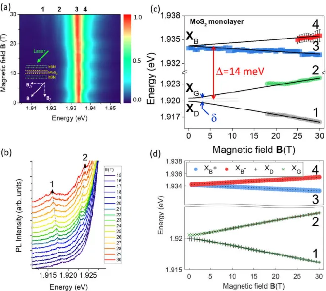
Finally we have measured the excitons spectra of MoS2 ML in tilted magnetic field. Due to the larger PL linewidth compared to the one of MoSe2 ML, it is more difficult to evidence the 4 excitons states as in Fig. 3a. However the energy of the two Zeeman split dark states can be extracted above 15 T as shown in Fig. 4(a) and 4(b). Fig. 4(c) displays the measured magnetic field dependence of the energies of the four states together with the fit based on the same model as MoSe2. Using =+14.0 meV and g// =2 (determined previously in the Voigt geometry), the best fit is obtained for =-1.8 and =-6.5. The bright exciton g-factor of about -2 was already measured in high quality MoS2 monolayer28 . However this is here the first measurement of the dark exciton g factor. Interestingly, we note that the g factors of both bright and dark excitons are significantly smaller in MoS2 than in other TMD materials. We can speculate that this is due to the very small conduction band spin-orbit splitting. Similarly, to MoSe2, the fit is not sensitive to the value of the dark-grey splitting due to the lack of experimental data at low field (the calculation has been done for meV). Table I summarizes the parameters of the exciton fine structure of MoS2 and MoSe2 monolayers presented in this Letter, together with the ones of WS2 and WSe2 MLs from previous work.
Discussion
The measured value of 14 meV in MoS2 ML generates several remarks and interrogations.
(i) First it demonstrates the key role played by the exciton exchange energy contribution to the bright-dark energy splitting. The bright-bright-dark exciton splitting includes three contributions18,19,17 :
=SO +bind +exch. , where SO is the conduction band spin-orbit splitting,bind is the difference between the binding energies of bright and dark excitons due to the slightly different masses of spin ↑ and spin ↓ conduction bands andexch is the short range exciton exchange energy. Although the actual value of the spin-orbit splitting is not yet known, the most widely used calculated value in the literature is SO = -3 meV29. In a first approximation, the binding energy is proportional to the reduced mass of the exciton. Taking the calculated effective masses from Ref29and the experimental value of the bright exciton binding energy from Ref 30 we infer bind = +8 meV. As a consequence our measurement of
=+14 meV demonstrates that the exciton exchange energy is crucial to determine the amplitude and the sign of the bright-dark energy splitting. Thus we deduce exch ~ +9 meV (if indeed SO =-3 meV and bind = +8 meV). Note that the CB spin-orbit splitting in MoS2 monolayer has been recently estimated from transport measurements31 ; a splitting of about 15 meV was measured for an electron density of a few 1012 cm-2. This value 5 times larger than the calculated one includes significant band renormalization induced by many body effects.
(ii) Importantly our measurements show that the splitting between spin-forbidden bright and dark excitons in MoS2 ML has an opposite sign compared to the calculated spin-orbit splitting in the conduction band. This could have important consequences for the trion fine structure32 .
(iii) Our measurements raise the question of the simple interpretation of MoS2 as a “bright” material. Indeed the TMD monolayers are usually divided into two categories: the so-called “dark” materials such as WS2 and WSe2 MLs where the spin-forbidden dark excitons lie at lower energy compared to the bright ones. As a consequence these monolayers are characterized by a rather weak luminescence yield at low temperature while the intensity increases with temperature due to thermal activation of bright states6,7,8,9. In contrast MoX2 monolayer (X=S, Se or Te) are often considered as “bright” materials as they exhibit stronger PL intensity at low temperature than their W-based counterparts but their intensity drops with temperature. This difference was assumed to vouch for dark excitons lying above the bright ones in MoX2. This bright-dark ordering has indeed been observed very recently for MoSe2 ML20 and confirmed by our results presented above. The measurements displayed in Fig. 1 show that the ordering is surprisingly opposite in MoS2 ML although the temperature dependence of the PL intensity in MoS2 ML is very similar to MoSe2 (strong at low temperature and decrease when temperature increases). Thus we cannot use this simple argument to distinguish between a “bright” and a “dark” material as our results prove that the dependence of PL intensity with temperature in MoS2 may be the result of a complex relaxation scheme between bright and dark states as well as its
interplay with non-radiative channels.
In addition, one can wonder why the grey exciton cannot be detected at zero magnetic field using high numerical aperture objective like in WS2 and WSe212 (see SI5). Remarkably we note in Fig. 1 that the PL intensity of the mixed dark-bright state in transverse magnetic field is very weak (compared to similar experiments performed in WS2 or WSe2 MLs12,13) and that very high field are required to sizably observe it (larger than 14 T). We can speculate that either the oscillator strength of grey exciton is much smaller than in WX2 and/or that their population remains weak despite lying at lower energy than the bright state. We can tentatively explain the small oscillator strength by noticing that the smaller spin-obit interaction in MoS2 compared to WS2 or WSe2 may yield a weaker oscillator strength of the grey exciton since it is related to the spin-orbit mixing with higher energy bands12,19. For the population issue, we can notice that contrary to WX2, the bright-dark exciton splitting in MoS2 ML is smaller than the optical phonon energies which can lead to inefficient relaxation between bright and dark excitons (the Γ5
phonon that permit relaxation from bright to dark exciton is 36 meV)3, 33.
Another striking difference between TMD materials is the amplitude of spin/valley polarization for excitons. While strong valley polarization and valley coherence have been measured in WSe2, WS2 and MoS2 MLs, the polarization in MoSe2 and MoTe2 MLs is very weak 34,35except under quasi-resonant excitation where significant polarization has been measured for the trion in MoSe236. Recently, it was
proposed that a crossing of bright and dark exciton dispersion curves combined with a Rashba effect associated with local fluctuations of electric field can lead to very fast spin relaxation11 . Our measurements of bright dark splitting in MoS2 and MoSe2 are perfectly consistent with this scenario:
the small negative splitting =-1.4 meV in MoSe2 combined with a larger effective mass for dark excitons should lead to a crossing between bright and dark dispersions while the positive splitting =+14 meV in MoS2 guarantees no crossing and as a consequence significant spin/valley exciton polarization measured in MoS2 MLs under CW optical orientation experiments 37,38,39.
In conclusion we have performed magneto-photoluminescence experiments in transverse and tilted magnetic fields up to 30 T in high quality MoS2 and MoSe2 monolayers. These investigations yield the unambiguous determination of the bright-dark exciton splitting and the dark exciton g-factor. Such fundamental parameters are key elements to understand the optoelectronic and spin/valley properties of these 2D semiconductors as well as their associated van der Waals heterostructures. Methods.
We fabricated high-quality samples by encapsulating MoS2 and MoSe2 MLs in hexagonal boron nitride
(hBN). The heterostructures are fabricated onto SiO2 (80 nm)/Si substrates. Details on sample
fabrication can be found in the Supplementary Information (SI) and in Refs12,40 .
Magneto-PL experiments at 4.2 K are performed in the Voigt configuration (magnetic field parallel to the layer plane) or tilted configuration (field oriented 45° with respect to the ML plane) using an optical-fiber-based insert placed in a high static magnetic field resistive magnet producing fields up to 30 T (see SI1).
Acknowledgements.
We acknowledge funding from ANR 2D-vdW-Spin, ANR VallEx, ANR MagicValley, ANR Graskop (ANR-19-CE09-0026) projects, Labex NEXT projects VWspin and MILO, EU Graphene Flagship project (no.785219), ATOMOPTO project (TEAM programme of the Foundation for Polish Science, co-financed by the EU within the ERD Fund), National Science Centre, Poland (grant no.UMO-2018/31/B/ST3/02111), and ME-YS-Czech Republic CEITEC 2020 (LQ1601) project. K.W. and T.T. acknowledge support from the Elemental Strategy Initiative conducted by the MEXT,Japan and and the CREST (JPMJCR15F3), JST. X. M. also acknowledges the Institut Universitaire de France. * CR, BH and PK contributed equally to this work.
† Corresponding Authors : cerobert@insa-toulouse.fr, bhan@insa-toulouse.fr, clement.faugeras@lncmi.cnrs.fr,
MoS2 MoSe2 WSe2 WS2
Splitting between bright and dark exciton (meV)
+14 -1.4 +4012,15 +5512
Splitting between grey and dark excitons (meV) < 2 < 1 0.621,27 - Bright exciton g factor -1.8 -4.0 -4.2541 -4.030 Dark exciton g factor -6.5 -8.6 -9.421,27 - Transverse electron g factor 2 2 2 -
Figure 1 -In-plane magnetic field B// – Spin-forbidden dark exciton in MoS2 monolayer encapsulated in hBN revealed by photoluminescence. (a) Color map of the variation of the PL intensity as a function of B// (the PL intensity of the bright exciton has been normalized at each field); (b) PL spectra for magnetic fields from 0 to 30 T showing the emergence of the brightened dark exciton at low energy. (c) Ratio of the PL intensity of dark (XD) and bright (XB) excitons as a function of magnetic field. Inset: sketch of the excitonic fine structure. The arrows ↑ and ↓ represent the main spin contribution of conduction and valence electrons involved in the exciton states (see Ref. 21 for more details).
Figure 2 -In-plane magnetic field B// – Spin-forbidden dark exciton in MoSe2 monolayer encapsulated in hBN revealed by photoluminescence. (a) Color map of the variation of the PL intensity as a function of B// (the PL intensity of the bright exciton has been normalized at each field); (b) Energy of dark and bright excitons as a function of B//. The solid lines correspond to the fit described in the text.
Figure 3 – Tilted (45°) magnetic field – The four mixed excitons states (labelled 1, 2, 3, 4) in MoSe2
monolayer revealed by magneto-photoluminescence. (a) Color map of the variation of the PL intensity as a function of B; (b) PL spectra for magnetic fields from 0 to 30 T showing the emergence of the four mixed states (the intensity is normalized to the main exciton line (state 2)). (c) Magnetic field dependence of the energy of the four mixed exciton states. The full lines are fits to the model described in the text. The notations dark exciton (XD), grey exciton (XG) and bright excitons (XB) are only strictly
valid at 0 T. (d) Same fitting results than in (c). The size of each symbol is proportional to the weight of each component (the two bright component XB+ and XB- and the two dark component XG and XD) (See
Figure 4 – Tilted (45°) magnetic field – The four mixed excitons states (labelled 1, 2, 3, 4) in MoS2
monolayer revealed by magneto-photoluminescence. (a) Color map of the variation of the PL intensity as a function of B; (b) PL spectra for magnetic fields from 15 to 30 T showing the emergence of the two lowest energy states 1 and 2 (mainly with grey and dark components). (c) Magnetic field dependence of the energy of the four mixed exciton states. The full lines are fits to the model described in the text. The notations dark exciton (XD), grey exciton (XG) and bright excitons (XB) are only strictly valid at 0 T.
(d) Same fitting results than in (c). The size of each symbol is proportional to the weight of each component (the two bright component XB+ and XB- and the two dark component XG and XD) (See SI8
References :
1 G. Wang, A. Chernikov, M. Glazov, T. Heinz, X. Marie, T. Amand, B. Urbaszek, Review of Modern Physics 90, 21001 (2018)
2 A. Jones, H. Yu, N. J. Ghimire, S. Wu, G. Aivazian, J.S. Ross, B. Zhao, J. Yan, D. G. Mandrus, D. Xiao, W. Yao, X. Xu, Nature Nano. 8, 634 (2013)
3 H. Dery, Y. Song, Phys. Rev. B 92, 125431 (2015)
4 P. Back, S. Zeytinoglu, A. Ijaz, M. Kroner, A. Imamoglu, Phys. Rev. Lett. 120, 37401 (2018)
5 M. Koperski, M. R. Molas, A. Arora, K. Nogajewski, A. O. Slobodeniuk, C. Faugeras, M. Potemski
Nanophotonics 6, 1289 (2017)
6 G. Wang, C. Robert, A. Suslu, B. Chen, S. Yang, S. Alamdari, I. Gerber, T. Amand, X. Marie, S. Tongay, B. Urbaszek, Nat. Commun. 6, 10110 (2015).
7 X-X. Zhang, Y. Yumeng, S. Zhao, F. Yang, T. Heinz, Phys. Rev. Lett. 115, 257403 (2015)
8 F. Withers O. Del Pozo-Zamudio, S. Schwarz, S. Dufferwiel, P.M. Walker, T. Godde, A. Rooney, A. Gholinia, C.R. Woods, P. Blake, S.J. Haigh, K. Watanabe, T. Taniguchi, I.L. Aleiner, A.K. Geim, V.I. Falko, A.I. Tartakovskii, K.S. Novoselov, Nano Lett. 15, 8223 (2015).
9 A. Arora, M. Koperski, K. Nogajewski, J. Marcus, C. Faugeras, M. Potemski, Nanoscale 7, 10421 (2015).
10 A. Vinattieri, J. Shah, T. C. Damen, D. S. Kim, L. N. Pfeiffer, M. Z. Maialle, L. J. Sham et al, Phys. Rev. B 50, 10868 (1993)
11 M. Yang, M. Yang, C. Robert, Z. Lu, D. Van Tuan, D. Smirnov, X. Marie, H. Dery et al, Arxiv 1909.03134 (2019)
12 G. Wang, C. Robert, M. M. Glazov, F. Cadiz, E. Courtade, T. Amand, D. Lagarde, T. Taniguchi, K.
Watanabe, B. Urbaszek and X. Marie, PRL 119, 047401 (2017)
13 M.R. Molas, C.Faugeras, A.O. Slobodeniuk, K. Nogajewski, M. Bartos, D.M. Basko, M. Potemski, 2D Mater. 4, 021003 (2017)
14 X. Zhang, T. Cao, Z. Lu, Y. Lin, F. Zhang, Y. Wang, Z. Li, J. C. Hone, J. A. Robinson, D. Smirnov, S. G. Louie & T.F. Heinz, Nature Nano 12, 883 (2017)
15 Y. Zhou, G. Scuri, D. S. Wild, A. A. High, A. Dibos, L. A. Jauregui, C. Shu, K. De Greve, K. Pistunova, A. Y. Joe, T. Taniguchi, K. Watanabe, P. Kim, M. D. Lukin & H. Park, Nature Nano 12, 856 (2017) | 16 E. Malic, M. Selig, M. Feierabend, S. Brem, D. Christiansen, F. Wendler, A. Knorr, G. Berghäuser, Phys. Rev. Mat 2, 014002 (2018)
17 T. Deilmann, K.Thygesen Phys. Rev. B 96, 201113(R) (2017) 18 D.Y. Qiu,T. Cao, S.G. Louie, Phys. Rev. Lett 115, 176801 (2015) )
19 J. P. Echeverry, B.Urbaszek, T. Amand, X. Marie, I.C. Gerber, Phys. Rev. B 93, 121107(R) (2016) 20 Z. Lu,D. Rhodes, Z. Li, D.V. Tuan, Z. Jiang , Z. Lian , S.F. Shi , J. Hone , H. Dery,D. Smirnov, 2D Mater. 7, 015017 (2020)
21 C. Robert, T. Amand, F. Cadiz, D. Lagarde, E. Courtade, M. Manca, T. Taniguchi, K. Watanabe, B. Urbaszek, X. Marie, Phys. Rev. B 96, 155423 (2017)
22 A O Slobodeniuk and D M Basko, 2D Materials 3, 035009 (2016)
23 T. Amand, X. Marie, P. Le Jeune, M. Brousseau, D. Robart, J. Barrau, R. Planel, Phys. Rev. Lett. 78, 1355 (1997)
24 I. V. Mashkov, C. Gourdon, P. Lavallard, and D. Yu Roditchev, Phys. Rev. B 55, 13761 (1997) 25 C. Robert, M. A. Semina, F. Cadiz, M. Manca, E. Courtade, T. Taniguchi, K. Watanabe, H. Cai, S. Tongay, B. Lassagne, P. Renucci, T. Amand, X. Marie, M. M. Glazov, and B. Urbaszek, Phys. Rev. Mat 2, 011001(R) (2018)
26 M. Koperski , M.R. Molas, A. Arora, K. Nogajewski, M. Bartos, J. Wyzula, D. Vaclavkova, P. Kossacki , M. Potemski, 2D Mater. 6 015001 (2019)
27 M.R. Molas, A. O. Slobodeniuk, T. Kazimierczuk, K. Nogajewski, M. Bartos, P. Kapuściński, K.
Oreszczuk, K. Watanabe, T. Taniguchi, C. Faugeras, P. Kossacki, D. M. Basko, and M. Potemski, Phys. Rev. Lett. 123, 096803 (2019).
28 F. Cadiz F. Cadiz, E. Courtade, C. Robert, G. Wang, Y. Shen, H. Cai, T. Taniguchi, K. Watanabe, H. Carrere, D. Lagarde, M. Manca, T. Amand, P. Renucci, S. Tongay, X. Marie and B. Urbaszek, Phys. Rev. X 7, 021026 (2017)
29 A. Kormanyos, G. Burkard, M. Gmitra, J. Fabian, V. Zólyomi, N. Drummond, V. Fal’ko et al, 2D Mater. 2 022001 (2015)
30 M. Goryca, J. Li, A.V. Stier, T. Taniguchi, K. Watanabe, E. Courtade, S. Shree, C. Robert,
B. Urbaszek , X. Marie & S.A. Crooker, Nature Com. 10, 4172 (2019)
31 R. Pisoni, A. Kormányos, M. Brooks, Z. Lei, P. Back, M. Eich, H. Overweg, Y. Lee, P. Rickhaus, K. Watanabe, T. Taniguchi, A. Imamoglu, G. Burkard, T.Ihn, K. Ensslin, Phys. Rev. Lett. 121, 247701 (2018)
32 J. Roch, G. Froehlicher, N. Leisgang, P. Makk, K. Watanabe, T. Taniguchi, R.Warburton, Nature Nano. 14, 432 (2019)
33 Z. Jin, X. Li, J.T. Mullen, K.W. Kim, Phys. Rev. B 90, 045422 (2014)
34 G. Wang, E. Palleau, T. Amand, S. Tongay, X. Marie, B. Urbaszek, APL 106, 112101 (2015)
35 C. Robert, R. Picard, D. Lagarde, G. Wang, J. P. Echeverry, F. Cadiz, P. Renucci, A. Ho ̈gele, T. Amand, X. Marie, I. C. Gerber, B. Urbaszek, Phys. Rev. B 94, 155425 (2016)
36 H. Tornatzky, A.-M. Kaulitz and J. Maultzsch, Phys. Rev. Lett. 121, 167401 (2018)
37 G. Sallen, L. Bouet, X. Marie, G. Wang, C. R. Zhu, W. P. Han, Y. Lu, P. H. Tan, T. Amand, B. L. Liu, and B. Urbaszek, Phys. Rev. B 86, 081301 (2012)
38 T. Cao, G.Wang, W. Han, H. Ye, C. Zhu, J. Shi, Q. Niu, P. Tan, E. Wang, B. Liu & J. Feng, Nat. Commun. 3, 887 (2012)
39 K. Mak, K. He, J. Shan, T. Heinz, Nat. Nano. 7, 494 (2012)
40 H.H. Fang, B. Han, C. Robert, M. A. Semina, D. Lagarde, E. Courtade, T. Taniguchi, K. Watanabe, T. Amand, B. Urbaszek, M. M. Glazov, and X. Marie, Phys. Rev. Lett. 123, 067401 (2019)
41 A.V Stier, N. P. Wilson, K. A. Velizhanin, J. Kono, X. Xu, and S. A. Crooker, Phys. Rev. Lett 120,