• Aucun résultat trouvé

A 10 000 fps CMOS Sensor With Massively Parallel Image Processing

N/A
N/A
Protected

Academic year: 2021

Partager "A 10 000 fps CMOS Sensor With Massively Parallel Image Processing"

Copied!
13
0
0

Texte intégral

(1)

HAL Id: hal-00482751

https://hal.archives-ouvertes.fr/hal-00482751

Submitted on 11 May 2010

HAL is a multi-disciplinary open access

archive for the deposit and dissemination of

sci-entific research documents, whether they are

pub-lished or not. The documents may come from

teaching and research institutions in France or

abroad, or from public or private research centers.

L’archive ouverte pluridisciplinaire HAL, est

destinée au dépôt et à la diffusion de documents

scientifiques de niveau recherche, publiés ou non,

émanant des établissements d’enseignement et de

recherche français ou étrangers, des laboratoires

publics ou privés.

Image Processing

Jérôme Dubois, Dominique Ginhac, Michel Paindavoine, Barthélémy Heyrman

To cite this version:

Jérôme Dubois, Dominique Ginhac, Michel Paindavoine, Barthélémy Heyrman. A 10 000 fps CMOS

Sensor With Massively Parallel Image Processing. IEEE Journal of Solid-State Circuits, Institute

of Electrical and Electronics Engineers, 2008, 43 (3), pp.706-717. �10.1109/JSSC.2007.916618�.

�hal-00482751�

(2)

A 10 000 fps CMOS Sensor With Massively Parallel

Image Processing

Jérôme Dubois, Student Member, IEEE, Dominique Ginhac, Member, IEEE, Michel Paindavoine, Member, IEEE,

and Barthélémy Heyrman

Abstract—A high-speed analog VLSI image acquisition and

pre-processing system has been designed and fabricated in a 0.35 m standard CMOS process. The chip features a massively parallel architecture enabling the computation of programmable low-level image processing in each pixel. Extraction of spatial gradients and convolutions such as Sobel or Laplacian filters are implemented on the circuit. For this purpose, each 35 m 35 m pixel in-cludes a photodiode, an amplifier, two storage capacitors, and an analog arithmetic unit based on a four-quadrant multiplier archi-tecture. The retina provides address-event coded output on three asynchronous buses: one output dedicated to the gradient and the other two to the pixel values.

A 64 64 pixel proof-of-concept chip was fabricated. A dedi-cated embedded platform including FPGA and ADCs has also been designed to evaluate the vision chip. Measured results show that the proposed sensor successfully captures raw images up to 10 000 frames per second and runs low-level image processing at a frame rate of 2000 to 5000 frames per second.

Index Terms—CMOS image sensor, parallel architecture,

high-speed image processing, analog arithmetic unit.

I. INTRODUCTION

T

ODAY, improvements in the growing digital imaging world continue to be made with two main image sensor technologies: charge coupled devices (CCD) and CMOS sensors. The continuous advances in CMOS technology for processors and DRAMs have made CMOS sensor arrays a viable alternative to the popular CCD sensors. New technolo-gies provide the potential for integrating a significant amount of VLSI electronics into a single chip, greatly reducing the cost, power consumption, and size of the camera [1]–[4], This advantage is especially important for implementing full image systems requiring significant processing such as digital cameras and computational sensors [5]–[7].

Most of the work on complex CMOS systems deals with the integration of sensors providing a processing unit at chip level (system-on-chip approach) or at column level by integrating an array of processing elements dedicated to one or more columns [8]–[11]. Indeed, pixel-level processing is generally dismissed because pixel sizes are often too large to be of practical use. However, as CMOS image sensors scale to 0.18 m processes and under, integrating a processing element at each pixel or group of neighboring pixels becomes feasible. More signif-icantly, employing a processing element per pixel offers the

Manuscript received May 8, 2007; revised October 2007.

The authors are with the LE2I Laboratory, Burgundy University, 21078 Dijon, France (e-mail: dginhac@u-bourgogne.fr).

Digital Object Identifier 10.1109/JSSC.2007.916618

opportunity to achieve massively parallel computations and thus the ability to exploit the high-speed imaging capability of CMOS image sensors [12]–[15]. This also benefits the implementation of new complex applications at standard rates and improves the performance of existing video applications such as motion vector estimation [16]–[18], multiple capture with dynamic range [19]–[21], motion capture [22], and pattern recognition [23].

As integrated circuits keep scaling down following Moore’s Law, recent trends show a significant number of papers dis-cussing the design of digital pixels [24]–[27] that take advan-tage of the increasing number of available transistors at the pixel in order to perform analog to digital conversion. This trend is mainly motivated by the significant advantages of pixel-level analog-to-digital (A/D) conversion such as high SNR, lower power consumption, and very low conversion speeds. Neverthe-less, the resulting implementations of in-pixel analog-to-digital converter (ADC) are rather area consuming, strongly restricting the image processing capability of CMOS sensors.

In this paper, we discuss hardware implementation issues of a high-speed CMOS imaging system embedding low-level image processing. For this purpose, we designed, fabricated, and tested a proof-of-concept 64 64 pixel CMOS analog sensor with per-pixel programmable processing element in a standard 0.35 m double-poly quadruple-metal CMOS technology. The main ob-jectives of our design are: 1) to evaluate the speed of the sensor, and, in particular, to reach a 10 000 frames/s rate; 2) to demon-strate a versatile and programmable processing unit at pixel-level; and 3) to provide an original platform dedicated to em-bedded image processing.

The rest of the paper is organized as follows. Section II is ded-icated to the description of the operational principle at pixel-level in the sensor. The main characteristics of the sensor ar-chitecture are described in Section III. Section IV talks about the design of the circuit. The details of the photodiode struc-ture, the embedded analog memories, and the arithmetic unit are successively described. Finally, some experimental results of high-speed image acquisition with pixel-level processing are presented in Section V.

II. EMBEDDEDALGORITHMS ATPIXELLEVEL

Low-level image processing consists of simple operations ex-ecuted on a very large data set, such as the whole set of pixel values or a region of interest of the whole image. Embedding low-level tasks at focal plane is quite interesting for several as-pects. First, the key features are the capability to operate in ac-cordance with the principles of single instruction multiple data (SIMD) computing architectures [13]. This enables massively

(3)

parallel computations allowing high framerates up to thousands of images per second, with a rather low power consumption. Morever, the parallel evaluation of the pixels by the SIMD op-erators leads to processing times which are not dependent of the resolution of the sensor. In a classical system, in which low-level filters are externaly implemented after digitization, processing times are proportional to the resolution leading to lower fram-erates as resolution increases. Secondly, having hardware pro-cessing operators, along with the sensor’s array, enables to re-move the classical input output bottleneck between the sensor and the external processors in charge of processing the pixel values. Indeed, the bandwith of the communication between the sensor and the external processors is known as a crucial aspect, especially with high-resolution sensors. In such cases, the sensor output data rate can be very high, and needs a lot of hardware ressources to convert, process and transmit a lot of in-formation. So, integrating image processing at the sensor level can solve this problem because the pixel values are pre-pro-cessed on-chip by the SIMD operators before sending them to the external world via the communication channel. This will re-sult in data reduction, which allows sending the data at lower data-rates, and reduces the effect of the computational-load bot-tleneck.

Thirdly, one of the main drawbacks to design specific circuits integrating sensing and processing on the same chip is that the image processing operators are often designed for a specific ap-plication and not reusable in another context. On the other side, digital processors are characterized by an important versality and their easy programming. However, in our approach, a new analog processing architecture has been designed. It highlights a compromise between versality, parallelism, processing speeds and resolution. The analog processing operators are fully pro-grammable devices by dynamic reconfiguration, They can be viewed as a software-programmable image processor dedicated to low-level image processing.

From a traditional point of view, a CMOS smart sensor can be seen as an array of independent pixels, each including a photodetector (PD) and a processing element (PE) built upon a few transistors. Existing works on analog pixel-level image processing can be classified into two main categories. The first one is intrapixel, in which processing is performed on the indi-vidual pixels in order to improve image quality, such as the clas-sical Active Pixel Sensor or APS [8], [28] as shown in Fig. 1(a). The second category is interpixel, where the processing is ded-icated to groups of pixels in order to perform some early vision processing and not merely to capture images. The transistors, which are placed around the photodetector, can be seen as a real on-chip analog signal processor which improves the func-tionality of the sensor. This typically allows local and/or global pixel calculations. Our work takes place in this second category because our main objective is the implementation of various in

situimage processing using local neighborhoods (such as spa-tial gradients, and Sobel and Laplacian filters). Based on this design concept, this forces a re-thinking of the spatial distribu-tion of the processing resources, so that each computadistribu-tional unit can easily use a programmable neighborhood of pixels. Conse-quently, in our design each processing element takes place in the middle of four adjacent pixels, as shown in the Fig. 1(b). The

Fig. 1. Photosites with (a) intra-pixel and (b) inter-pixel processing.

Fig. 2. Evaluation of spatial gradients.

key to this distribution of the pixel-level processors is to realize both compactness of the metal interconnections with pixels and generality of high-speed processing based on neighborhood of pixels.

A. Spatial Gradients

The structure of our processing unit is tailor-made for the computation of spatial gradients based on a 4-neighborhood pixel algorithm, as depicted in Fig. 2.

The main idea for evaluating the spatial gradients [29] is based on the definition of the first-order derivative of a 2-D func-tion performed in the vector direcfunc-tion , which can be expressed as

(1) where is the vector’s angle of outline.

A discretization of (1) at the pixel-level, according to Fig. 2, would give

(2) where is the luminance at pixel i, i.e., the photo-diode output. In this way, the local derivative in the direction of vector is continuously computed as a linear combination of two basis functions, the derivatives in the and directions.

(4)

Fig. 3. Implementation of multipliers at pixel-level.

Fig. 4. (a) Array architecture. (b) 3 3 mask used by the four processing ele-ments.

Using a four-quadrant multiplier [30], [31] (see Section IV-C for details of design and implementation), the product of the deriva-tives by a cosine function can easily be computed. The output product , as shown in Fig. 3, is given by

(3) Consequently, the processing element implemented at the pixel-level carries out a linear combination of the four adjacent pixels by the four associated weights . In order to evaluate (3), the following values have to be given to the coefficients:

(4) From such a viewpoint, horizontal and vertical gradients can be straightforwardly evaluated by respectively fixing the value of as 0 and 90 .

B. Sobel Operator

The structure of our architecture is also well-adapted to var-ious algorithms based on convolutions using binary masks on a neighborhood of pixels. For example, the evaluation of the Sobel algorithm with our chip leads to the result directly centered on the photosensor and directed along the natural axes of the image according to Fig. 4(a). In order to compute the mathematical op-eration, a 3 3 neighborhood is applied on the whole image, as described in Fig. 4(b).

Fig. 5. Schematic imager system bloc.

In order to carry out the discretized derivatives in two dimen-sions (along the horizontal and vertical axes) it is necessary to build two 3 3 matrices called and :

(5) Within the four processing elements numbered from 1 to 4, as shown in Fig. 4(a), four 2 2 masks act locally on the image. According to (5), this allows the evaluation of the following series of operations:

(6) with the values and provided by the processing element . Then, from these trivial operations, the discrete amplitudes of the derivatives along the vertical axis

and the horizontal axis

can be computed. The evaluation of the horizontal and vertical gradients spends four retina cycles, two for each gradient.1

In the first frame, in order to evaluate , the following values have to be given to the coefficients:

(7) Then, in the second frame is evaluated by using the following coefficient values:

(8) So, the Analog Arithmetic Units (A U) implementing these computations at pixel-level (see Section IV-B for details) dras-tically decrease the number of calculation carried out by the external processor (FPGA) as shown in Fig. 5. Indeed, in the

1A retina cycle is defined as the time spent between two successive acquisition

(5)

Fig. 6. Dynamic reconfiguration sequence for vertical Sobel filter.

case of our experimental 64 64 pixel sensor, the peak per-formance is equivalent to 4 parallel signed multiplications by pixel at 10 000 frames/s, i.e., more than 160 million multiplica-tions per second. With a VGA resolution (640 480), the per-formance level would increase to a factor of 75, leading to about 12 billion multiplication per second. Processing this data flow by external processors will imply important hardware resources in order to cope with the temporal constraints.

Moreover, with our chip, the assignment of coefficient values from the external processor towards the retina, gives the system some interesting dynamic properties. The system can be easily reconfigured by changing the internal coefficients for the masks between two successive frames. First, this allows the possibility to dynamically change the image processing algorithms em-bedded in the sensor. Second, this enables the evaluation of some complex pixel-level algorithms, implying different suc-cessive convolution masks. For example, as depicted in Fig. 6, the coefficient values are reconfigured twice in order to evaluate the vertical Sobel filter. During the first frame, and are evaluated whereas the second frame allows the computation of and . The FPGA is only used for the final addition of the four values.

C. Second-Order Detector: Laplacian

Edge detection based on some second-order derivatives such as the Laplacian can also be implemented on our architecture. Unlike previously described spatial gradients, the Laplacian is a scalar [see (9)] and does not provide any indication about edge direction:

(9) From this 3 3 mask, the following operations can be ex-tracted according to the principles previously used for the eval-uation of the Sobel operator:

(10)

The discrete amplitudes of the second-order derivative is given by . These operations can be carried out in four retina cycles.

D. General Spatial Filter and Strategies

In the preceding sections, we focused on 2 2 and 3 3 con-volution masks. In the case of a 2 2 mask, the coefficients are fixed once before the beginning of the acquisition frame. In the case of a 3 3 mask, two possibilities can occur. First, the 3 3 mask presents some symmetrical properties (such as the Sobel or Laplacian masks) and then the coefficients values can be fixed as in a 2 2 mask. Second, if the mask is not symmetric, it is necessary to dynamically reconfigure the coefficients during the acquisition frame. For masks which size is greater than 3 3 and more generally in the case of an N N mask, a dynamic reconfiguration of coefficients is necessary during the acquisi-tion frame in order to evaluate the successive values of the linear combinations of pixels.

III. OVERVIEW OF THECHIPARCHITECTURE

As in a traditional image sensor, the core of the chip pre-sented in this paper is constructed of a 2-D pixel array, here of 64 columns and 64 rows with random pixel ability, and some peripheral circuits. It contains about 160 000 transistors on a 3.675 mm 3.775 mm die. The full layout of the retina is de-picted in Fig. 7 and the main chip characteristics are listed in Table I.

Each individual pixel contains a photodiode for the light-to-voltage transduction and 38 transistors integrating all the analog circuitry dedicated to the image processing algorithms. This amount of electronics includes a preloading circuit, two Analog Memory, Amplifier and Multiplexer structures ([AM] ) and an Analog Arithmetic Unit (A U) based on a four-quadrant multi-plier architecture. The full pixel size is 35 m 35 m with a 25% fill factor.

Fig. 8 shows a block diagram of the proposed chip. The ar-chitecture of the chip is divided into three main blocks as in many circuits widely described in the literature. First, the array of pixels (including photodiodes with their associated circuitry for performing the analog computation) is placed at the center. Second, placed below the chip core are the readout circuits with the three asynchronous output buses: the first one is dedicated

(6)

Fig. 7. Layout of the full retina.

TABLE I CHIPCHARACTERISTICS

Fig. 8. Block diagram of the chip.

to the image processing results whereas the other two provide parallel outputs for full high rate acquisition of raw images. Fi-nally, the left part of the sensor is dedicated to a row decoder for addressing the successive rows of pixels. The pixel values are selected one row at a time and read out to vertical column buses connected to an output multiplexor.

The chip also contains test structures used for detailed char-acterization of the photodiodes and processing units. These test structures can be seen on the bottom left of the chip.

The operation of the imaging system can be divided into four phases: reset, integration, image processing, and readout. The reset, integration, and pixel-level processing phases all occur in parallel over the full array of pixels (snapshot mode) in order to avoid any distortion due to a row-by-row reset. The control of the integration time can be supervised with the global output signal called Out int. This signal provides the average incidental illumination of the whole matrix of pixels. Indeed, the currents issued from all the pixels of the matrix are summed to produce Out int. So, this signal is directly linked to the average level of the image. A low value of Out int implies a dark image, whereas an important value traduces a bright image. Following the values of Out int, the integration time can be adapted in order to obtain the most appropriate images: if the average level of the image is too low, the exposure time may be increased. On the contrary, if the scene is too luminous, the integration period may be re-duced.

IV. DESIGN OF THECIRCUIT

A. Photodiode Structure

As previously described in Section II, each pixel of our chip includes a photodiode and a processing unit dedicated to low-level image processing based on neighborhoods. One of our main objectives focuses on the optimization of the pixel-level processor mapping in order to facilitate the access to the values of adjacent pixels. Therefore, an original structure [as previ-ously depicted in Fig. 1(b)] was chosen. The major advantage of this structure is the minimization of the length of metal in-terconnection between adjacent pixels and the processing units, contributing to: 1) a better fill factor and 2) a higher framerate.

In order to achieve high-speed performance, one of the key elements is the photodiodes which should be designed and op-timized carefully. Critical parameters in the design of photo-diodes are the dark current and the spectral response [32]. The shape of photodiode layout, the structure of the photodiode, and the layout have significant influences on the performance of the whole imager [33], [34].

In our chip, photodiodes consist of N-type photodiodes based on an n -type diffusion in a p-type silicon substrate. The depletion region is formed in the neighborhood of the photodiode cathode. Optically generated photocarriers diffuse to neighboring junctions [35]. We have analyzed and tested three photodiodes shapes: the square photodiode classically used in literature, the cross shape which is perfectly adapted to the optimized pixel-level processors mapping, and finally the octagonal shape based on 45 structures.

Fig. 9 illustrates these different photodiodes structures. For each of these shapes, the active area (displayed in gray dots) and the inter-element isolation area with external connections (filled in gray) are represented. The active area absorbs the illu-mination energy and turns that energy into charge carriers. This active area must be large as possible in order to absorb a max-imum of photons whereas the inter-element isolation area must be as small as possible in order to obtain the best fill factor (i.e., the ratio between the active area and the total pixel area). In the follow-up to this paper, we use the term Active layer surfaces ( ) when talking about the active area of the photodiode and

(7)

Fig. 9. Photodiode structures. (a) Square shape. (b) Cross shape. (c) Octagonal shape.

Fig. 10. for the three different shapes expressed as a function of the side of the square photodiode.

the term Connection layers surfaces ( ) for the connections of the photodiodes. Based on the geometrical parameters , and , we can easily define the and mathematical ex-pressions (as depicted in the Fig. 10). Furthermore, according to the design rules of the AMS-CMOS 0.35 m process, the min-imal value of was evaluated to 2.35 m. Starting from this result, we can plot comparative graphs of for the three pho-todiodes shapes, as shown in Fig. 10.

In our design, we have fixed the fill factor to 25% with a total pixel size of 35 m 35 m. So, the values of and can be easily inferred: m and m. From Fig. 10, we can see 1) that the cross shape appears to be un-realistic because of the large value of m ) and 2) that the square and the octagonal shapes have similar values (respectively, 191 m and 173 m ). Finally, the octag-onal shape was chosen because the surface dedicated to the in-terconnections is about 12% lower compared to a square shape, allowing a best integration of the photodiodes. This also im-plies a better spectral response compared to the square photo-diode as shown in Fig. 11. A detailed characterization of spectral responses of the different photodiodes has been performed by using a light generator with wavelength of 400 nm to 1100 nm. The experimental data reveal that the octagonal structure has better performance than the square shape for all wavelengths. Our results are complementary and similar to those obtained by [33] in their study of dark current.

Fig. 11. Spectral responses in the photodiode structures of type square, and type octagonal.

Fig. 12. (a) Array of pixel based on octagonal photodiodes. (b) Evaluation of spatial gradients.

From the above measurement results, the octagonal type pho-todiode structure was chosen as the photodetector for our chip. Fig. 12 illustrates the arrangement of pixels and the computation of spatial gradients in this configuration, as previously described in this paper.

B. Pixel-Level [AM]

In order to increase the algorithmic possibilities of the archi-tecture, the key point is the separation of the acquisition of the light inside the photodiode and the readout of the stored value at pixel-level [36]. Thus, the storage element should keep the output voltage of the previous frames whereas the sensors in-tegrate photocurrent for a new frame. So, for each pixel of our chip we have designed and implemented two specific circuits, including an analog memory, an amplifier, and a multiplexor as shown in Fig. 14.

With these [AM] circuits, the capture sequence can be made in the first memory in parallel with a readout sequence and/or processing sequence of the previous image stored in the second memory, as shown in Fig. 13.

Such a strategy has several advantages:

1) The framerate can be increased (up to 2x) without reducing the exposure time.

(8)

Fig. 14. Schematic of the [AM] structure.

Fig. 13. Parallelism between capture sequence and readout sequence.

2) The image acquisition is decorrelated from image pro-cessing, implying that the architecture performance is always the highest, and the processing framerate is max-imum.

3) A new image is always available without spending any in-tegration time.

The chip operates with a single 3.3 V power supply. In each pixel, as shown in Fig. 14, the photosensor is a nMOS photo-diode associated with a pMOS transistor reset, which represents the first stage of the acquisition circuit. The pixel array is held in a reset state until the init signal goes high. Then, the photodiode discharges according to incidental luminous flow. This signal is polarized around (i.e., half the power supply voltage). Behind this first stage of acquisition, two identical subcircuits take place. One of these subcircuits is selected when either the

store1signal or the store2 signal is turned on. Then, the associ-ated analog switch is open allowing the capacitor to integrate the pixel value. Consequently, the capacitors are able to store the pixel values during the frame capture either from switch 1 or switch 2. The capacitors are implemented with double-polysili-cium. The size of the capacitors is as large as possible in order to respect the fill factor and the pixel size requirements. The ca-pacitors values are about 40 fF and are able to store the pixel values for 20 ms with an error lower than 4% Each of the ca-pacitors is followed by an inverter, polarized on . This

Fig. 15. The A U structure.

inverter serves as an amplifier of the stored value. It provides a value which is proportional to the pixel incidental illumination. Finally, the readout of the stored values are activated by a last switch controlled by the read1 and read2 signals.

C. Pixel-Level Analog Arithmetic Unit: A U

The analog arithmetic unit (A U) represents the central part of the pixel and includes four multipliers (M1, M2, M3, and M4), as illustrated in Fig. 15. The four multipliers are all inter-connected with a diode-inter-connected load (i.e., an nMOS transistor with gate connected to drain). The operation result at the node point is a linear combination of the four adjacent pixels.

Assuming that MOS transistors operate in subthreshold re-gion, the output node of a multiplier can be expressed as a function of the two inputs and as follows:

(11) where represents the transconductance ratio, and are the threshold voltage for the nMOS and pMOS transistors. Around the operating point , the variations of the output node mainly depend on the product . So, (11) can be simplified and finally, the output node can be expressed as a simple first-order of the two input voltages and :

with (12)

The important value of the coefficient gives to the structure a good robustness by limiting the impact of the second-order intermodulation products. The first consequence is a better lin-earity of our multiplier design integrating only five transistors.

(9)

Fig. 16. Benchmark of the four-quadrant multiplier.

Fig. 16 shows the experimental results of this multiplier struc-ture with cosine signals as inputs:

kHz (13) kHz (14) In an ideal case, the output node value can be written as fol-lows:

(15) The signal’s spectrum, represented in Fig. 16(b), contains two main frequencies (17.5 kHz and 22.5 kHz) around the car-rier frequency. The residues which appear in the spectrum are known as inter-modulations products. They are mainly due to the nonlinearity of the structure (around 10 kHz and 30 kHz) and the insulation defects of input pads (at 40 kHz). However, the amplitude of these inter-modulation products is significantly lower than the two main frequencies. Indeed, the spectral line level at 40 kHz is 9 dB under the level of the main frequen-cies. Therefore, the contribution of the insulation defect is eight times smaller than the main signals. Furthermore, experimental measures on the chip revealed that the best linearity of the mul-tiplier is obtained for amplitudes of the signal in the range of 0.6–2.6 V. In the chip, the signal corresponds to the voltage coming from the pixel. The pixel values can be included in this range by means of by the biasing voltage Vbias of the [AM] structure.

TABLE II CHIPMEASUREMENTS

V. EXPERIMENTALRESULTS

An experimental 64 64 pixel image sensor has been de-veloped in a 0.35 m, 3.3 V, standard CMOS process with poly-poly capacitors. This prototype was sent to foundry at the beginning of 2006 and was available at the end of the third quarter of the year. Its functional testing and its characterization were performed using a specific hardware platform. The hard-ware part of the imaging system contains a one million Gates Spartan-3 FPGA board with 32 MB SDRAM embedded. This FPGA board is the XSA-3S1000 from XESS Corporation. An interface acquisition circuit includes three ADC from Analog Device (AD9048), high-speed LM6171 amplifiers and others elements such as the motor lens. Fig. 17 shows the schematic and some pictures of the experimental platform.

A. Characterization

The sensor was quantitatively tested for conversion gain, sen-sitivity, fixed pattern noise, thermal reset noise, output levels disparities, voltage gain of the amplifier stage, linear flux, and dynamic range. Table II summarizes these imaging sensor char-acterization results. To determine these values, the sensor in-cluded specific test pixels in which some internal node voltages can be directly read. The test equipment hardware is based on a light generator with wavelength of 400 nm to 1100 nm. The sensor conversion gain was evaluated to 54 V/e RMS with a sensitivity of 0.15 V/lux s, thanks to the octagonal shape of the photodiode and the fill factor of 25%. At 10 000 frames/s, measured nonlinearity is 0.12% over a 2 V range. These perfor-mances are similar to the sensor described in [25]. According to the experimental results, the voltage gain of the amplifier stage of the two [AM] is and the disparities on the output levels are about 4.3 %.

Image sensors always suffer from technology related non-idealities that can limit the performances of the vision system. Among them, fixed pattern noise (FPN) is the variation in output pixel values, under uniform illumination, due to device and in-terconnect mismatches across the image sensor. Two main types of FPN occur in CMOS sensors. First, offset FPN which takes place into the pixel is due to fluctuations in the threshold voltage of the transistors. Second, the most important source of FPN is introduced by the column amplifiers used in standard APS sys-tems. In our approach, the layout is symmetrically built in order to reduce the offset FPN among each block of four pixels and

(10)

Fig. 17. Block diagram and pictures of the hardware platform including FPGA board and CMOS sensor.

Fig. 18. Layout of four pixels.

to ensure uniform spatial sampling, as depicted in the layout of a 2 2 pixel block in Fig. 18.

Furthermore, our chip does not include any column amplifier since the amplification of the pixel values takes place into the pixel by means of an inverter. So, the gain FPN is very limited and only depends on the mismatch of the two transistors. FPN can be reduced by correlated double sampling (CDS). To imple-ment CDS, each pixel output needs to be read twice, once after reset and a second time at the end of integration. The correct pixel signal is obtained by substracting the two values. A CDS can be easily implemented in our chip. For this purpose, the first analog memory stores the pixel value just after the reset signal and the second memory stores the value at the end of integra-tion. Then, at the end of the image acquisition, the two values can be transfered to the FPGA, responsible for producing the difference. In Fig. 19, the two images show fixed pattern noise with and without CDS using a 1 ms integration time. On the left image, the FPN is mainly due to the random variations in the offset voltages of the pixel-level analog structures. The experi-mental benchmarks of our chip reveal a FPN value of 225 V RMS. The right picture shows the same image after analog CDS, performed as described above. The final FPN has been reduced by a factor of 34 to 6.6 V. In the rest of the results, CDS has

Fig. 19. Images of fixed pattern noise (a) without CDS and (b) with CDS for an integration time of 1 ms.

Fig. 20. High-speed sequence capture with basic image processing.

not been implemented since FPN has low values. Only, an entire dark image is substracted from the output images on the FPGA. Focus has been made on the development of low-level image processing using the two analog memories and the associated processing unit.

(11)

Fig. 21. (a) Raw image at 10 000 fps. (b) Output Sobel horizontal image. (c) Output Sobel vertical image. (d) Output Laplacian image.

B. Sample Images

Fig. 20 describes the experimental results of successive acquisitions and signal processing in an individual pixel. Each acquisition occurs when one of the two signals read 1 or read

2 goes high. For each of these acquisitions, various levels of illumination are applied. The two outputs (out 1 and out 2 give a voltage corresponding to the incidental illumination on the pixels. The calibration of the structure is ensured by the biasing (Vbias 1.35 V). Moreover, in this characterization, the output

node computes the difference between out 1 and out2. For this purpose, the coefficients are fixed at the following values:

and .

Fig. 21 shows experimental image results. Fig. 21(a) shows an image acquired at 10 000 frames/s (integration time of 100 s). Except for amplification of the photodiodes signal, no other processing is performed on this raw image. Fig. 21(b)–(d) shows different images with pixel-level image processing at a frame rate of about 2500 frames/s. From left to right, horizontal and vertical Sobel filter and Laplacian operator images are displayed. Some of these image processing algorithms imply a dynamic reconfiguration of the coefficients. We can note that there is no energy spent for transferring information from one level of processing to another because only a frame acquisition is needed before the image processing take place.

In order to estimate the quality of our embedded image pro-cessing approach, we have compared results of horizontal and vertical Sobel and Laplacian operators obtained with our chip and with digital operators implemented on a computer. In each case, the image processing is applied on real images obtained by our chip. For the comparison of the results, we have evaluated the likelihood between the resulting images by using the cross correlation coefficient. The correlation coefficient is given by

(16) where is the resulting image obtained with the analog arith-metic units on the retina, and is the resulting image obtained with an external processor. and are respectively the average matrices and . is the array size . Table III summarizes the results of the cross correlation coefficient ob-tained with horizontal and vertical Sobel filters and Laplacian operators.

TABLE III

IMAGECORRELATIONCOEFFICIENT

The cross correlation coefficient can be viewed as a good in-dicator of the linearity of the pixel-level analog arithmetic units. In our case, this coefficient is 93.2% on average. The likelihood, specifically for the Laplacian operator, is greater because of the perfect symmetry of this operator. Overall, the analog arithmetic unit has good performance compared to external operators im-plemented on a computer.

VI. CONCLUSION ANDPERSPECTIVES

An experimental pixel sensor implemented in a stan-dard digital CMOS 0.35 m process was described. Each 35 m 35 m pixel contains 38 transistors implementing a circuit with photocurrent integration, two [AM] , and an A U. Experimental chip results reveal that raw image acquisition at 10 000 frames per second can be easily achieved using the parallel A U implemented at pixel-level. With basic image pro-cessing, the maximal frame rate slows to about 5000 fps.

The next step in our research will be the design of a similar circuit in a modern 130 nm CMOS technology. The main objec-tive will be to design a pixel of less than 10 m 10 m with a fill factor of 20%. Thus, with the increasing scaling of the tran-sistors in a such technology, we could consider the implemen-tation of more sophisticated image processing operators ded-icated to face localization and recognition. Previous works of our team [37] have demonstrated the needs of dedicated CMOS sensors embedding low-level image processing such as features extraction. Moreover, actual works [38] focus on a recent face detector called the Convolutional Face Finder (CFF) [39], which is based on a multi-layer convolutional neural architecture. The CFF consists of six successive neural layers. The first four layers extract characteristic features, and the last two perform the clas-sification. Our objective would be to implement at pixel-level the first layers based on convolutions by different masks from 2 2 to 5 5.

In order to evaluate this future chip in some realistic condi-tions, we would like to design a CIF sensor (352 288 pixels), which leads to a 3.2 mm 2.4 mm in a 130 nm technology. In

(12)

the same time, we will focus on the development of a fast ADC. The integration of this ADC on future chips will allow us to provide new and sophisticated vision systems on chip (ViSOC) dedicated to digital embedded image processing at thousands of frames per second.

REFERENCES

[1] E. Possum, “Active pixel sensors: Are CCDs dinosaurs?,” Int. Soc. Opt.

Eng. (SPIE), vol. 1900, pp. 2–14, 1993.

[2] E. Possum, “CMOS image sensor : Electronic camera on a chip,” IEEE

Trans. Electron Devices, vol. 44, no. 10, pp. 1689–1698, Oct. 1997. [3] P. Seitz, “Solid-state image sensing,” Handbook of Computer Vision

and Applications, vol. 1, pp. 165–222, 2000.

[4] D. Litwiller, “CCD versus CMOS: Facts and fiction,” Photonics

Spectra, pp. 154–158, Jan. 2001.

[5] M. Loinaz, K. Singh, A. Blanksby, D. Inglis, K. Azadet, and B. Ack-land, “A 200 mv 3.3 V CMOS color camera IC producing 352 288 24-b video at 30 frames/s,” IEEE J. Solid-State Circuits, vol. 33, no. 12, pp. 2092–2103, Dec. 1998.

[6] S. Smith, J. Hurwitz, M. Torrie, D. Baxter, A. Holmes, M. Panaghiston, R. Henderson, A. Murrayn, S. Anderson, and P. Denyer, “A single-chip 306 244-pixel CMOS NTSC video camera,” in IEEE ISSCC Dig.

Tech. Papers, San Francisco, CA, 1998, pp. 170–171.

[7] A. El Gamal, D. Yang, and B. Fowler, “Pixel level processing—why, what and how?,” in Proc. SPIE Electronic Imaging’99 Conf., Jan. 1999, vol. 3650, pp. 2–13.

[8] O. Yadid-Pecht and A. Belenky, “In-pixel autoexposure CMOS APS,”

IEEE J. Solid-State Circuits, vol. 38, no. 8, pp. 1425–1428, Aug. 2003. [9] P. Acosta-Serafini, M. Ichiro, and C. Sodini, “A 1/3 VGA linear wide dynamic range CMOS image sensor implementing a predictive mul-tiple sampling algorithm with overlapping integration intervals,” IEEE

J. Solid-State Circuits, vol. 39, no. 9, pp. 1487–1496, Sep. 2004. [10] L. Kozlowski, G. Rossi, L. Blanquart, R. Marchesini, Y. Huang, G.

Chow, J. Richardson, and D. Standley, “Pixel noise suppression via SoC management of target reset in a 1920 1080 CMOS image sensor,” IEEE J. Solid-State Circuits, vol. 40, no. 12, pp. 2766–2776, Dec. 2005.

[11] M. Sakakibara, S. Kawahito, D. Handoko, N. Nakamura, M. Higashi, K. Mabuchi, and H. Sumi, “A high-sensitivity CMOS image sensor with gain-adaptative column amplifiers,” IEEE J. Solid-State Circuits, vol. 40, no. 5, pp. 1147–1156, May 2005.

[12] A. Krymsky and T. Niarong, “A 9-V/Lux 5000-frames/s 512 512 CMOS sensor,” IEEE Trans. Electron Devices, vol. 50, no. 1, pp. 136–143, Jan. 2003.

[13] G. Cembrano, A. Rodriguez-Vazquez, R. Galan, F. Jimenez-Garrido, S. Espejo, and R. Dominguez-Castro, “A 1000 FPS at 128 128 vision processor with 8-bit digitized I/O,” IEEE J. Solid-State Circuits, vol. 39, no. 7, pp. 1044–1055, Jul. 2004.

[14] L. Lindgren, J. Melander, R. Johansson, and B. Mller, “A multireso-lution 100-GOPS 4-Gpixels/s programmable smart vision sensor for multi-sense imaging,” IEEE J. Solid-State Circuits, vol. 40, no. 6, pp. 1350–1359, Jun. 2005.

[15] Y. Sugiyama, M. Takumi, H. Toyoda, N. Mukozaka, A. Ihori, T. Kurashina, Y. Nakamura, T. Tonbe, and S. Mizuno, “A high-speed CMOS image with profile data acquiring function,” IEEE J. Solid-State

Circuits, vol. 40, pp. 2816–2823, 2005.

[16] D. Handoko, K. S, Y. Takokoro, M. Kumahara, and A. Matsuzawa, “A CMOS image sensor for local-plane motion vector estimation,” in

Symp. VLSI Circuits Dig. Papers, Jun. 2000, vol. 3650, pp. 28–29. [17] S. Lim and A. El Gamal, “Integrating image capture and

pro-cessing—beyond single chip digital camera,” in Proc. SPIE Electronic

Imaging 2001 Conf., San Jose, CA, Jan. 2001, vol. 4306.

[18] X. Liu and A. El Gamal, “Photocurrent estimation from multiple non-destructive samples in a CMOS image sensor,” in Proc. SPIE Electronic

Imaging 2001 Conf., San Jose, CA, Jan. 2001, vol. 4306.

[19] D. Yang, A. El Gamal, B. Fowler, and H. Tian, “A 640 512 CMOS image sensor with ultra wide dynamix range floating-point pixel-level ADC,” IEEE J. Solid-State Circuits, vol. 34, no. 12, pp. 1821–1834, Dec. 1999.

[20] O. Yadid-Pecht and E. Possum, “CMOS APS with autoscaling and cus-tomized wide dynamic range,” in IEEE Workshop on Charge-Coupled

Devices and Advanced Image Sensors, Jun. 1999, vol. 3650, pp. 48–51. [21] D. Stoppa, A. Somoni, L. Gonzo, M. Gottardi, and G.-F. Dalla Betta, “Novel CMOS image sensor with a 132-db dynamic range,” IEEE J.

Solid-State Circuits, vol. 37, no. 12, pp. 1846–1852, Dec. 2002.

[22] X. Liu and A. El Gamal, “Simultaneous image formation and motion blur restoration via multiple capture,” in Proc. IEEE Int. Conf.

Acous-tics, Speech and Signal Processing, 2001, vol. 3, pp. 1841–1844. [23] C.-Y. Wu and C.-T. Chiang, “A low-photocurrent CMOS retinal

focal-plane sensor with a pseudo-bjt smoothing network and an adaptative current schmitt trigger for scanner applications,” IEEE Sensors J., vol. 4, no. 4, pp. 510–518, Aug. 2004.

[24] D. Yang, B. Fowler, and A. El Gamal, “A Nyquist-rate pixel-level ADC for CMOS image sensors,” IEEE J. Solid-State Circuits, vol. 34, no. 3, pp. 348–356, Mar. 1999.

[25] S. Kleinfelder, S. Lim, X. Liu, and A. El Gamal, “A 10 000 frames/s CMOS digital pixel sensor,” IEEE J. Solid-State Circuits, vol. 36, no. 12, pp. 2049–2059, Dec. 2001.

[26] A. Harton, M. Ahmed, A. Beuhler, F. Castro, L. Dawson, B. Herold, G. Kujawa, K. Lee, R. Mareachen, and T. Scaminaci, “High dynamic range CMOS image sensor with pixel level ADC and in situ image enhancement,” in Sensors and Camera Systems for Scientific and

In-dustrial Applications VI. Proc. SPIE, Mar. 2005, vol. 5677, pp. 67–77. [27] Y. Chi, U. Mallik, E. Choi, M. Clapp, G. Gauwenberghs, and R. Etienne-Cummings, “Cmos pixel-level ADC with change detection,” in Proc. Int. Symp. Circuits and Systems (ISCAS), May 2006, pp. 1647–1650.

[28] O. Yadid-Pecht, B. Pain, C. Staller, C. Clark, and E. Possum, “CMOS active pixel sensor star tracker with regional electronic shutter,” IEEE

J. Solid-State Circuits, vol. 32, no. 2, pp. 285–288, Feb. 1997. [29] M. Barbara, P. Burgi, A. Mortara, P. Nussbaum, and F. Heitge, “A

100 100 pixel silicon retina for gradient extraction with steering filter capabilities and temporal output coding,” IEEE J. Solid-State Circuits, vol. 37, no. 2, pp. 160–172, Feb. 2002.

[30] C. Ryan, “Applications of a four-quadrant multiplier,” IEEE J.

Solid-State Circuits, vol. 5, no. 1, pp. 45–48, Feb. 1970.

[31] S. Liu and Y. Hwang, “CMOS squarer and four-quadrant multiplier,”

IEEE Trans. Circuits Syst. I, Fundam. Theory Applicat., vol. 42, no. 2, pp. 119–122, Feb. 1995.

[32] C. Wu, Y. Shih, J. Lan, C. Hsieh, C. Huang, and J. Lu, “Design, op-timization, and performance analysis of new photodiode structures for CMOS active-pixel-sensor (APS) imager applications,” IEEE Sensors

J., vol. 4, no. 1, pp. 135–144, Feb. 2004.

[33] I. Shcherback, A. Belenky, and O. Yadid-Pecht, “Empirical dark cur-rent modeling for complementary metal oxide semiconductor active pixel sensor,” Opt. Eng., vol. 41, no. 6, pp. 1216–1219, Jun. 2002. [34] I. Shcherback and O. Yadid-Pecht, “Photoresponse analysis and pixel

shape optimization for CMOS active pixel sensors,” IEEE Trans.

Elec-tron Devices, vol. 50, no. 1, pp. 12–18, Jan. 2003.

[35] J. Lee and R. Hornsey, “CMOS photodiodes with substrate openings for higher conversion gain in active pixel sensor,” in IEEE Workshop

on CCDs and Advanced Image Sensors, Crystal Bay, NV, Jun. 2001. [36] G. Chapinal, S. Bota, M. Moreno, J. Palacin, and A. Herms, “A

128 128 CMOS image sensor with analog memory for synchronous image capture,” IEEE Sensors J., vol. 2, no. 2, pp. 120–127, Apr. 2002. [37] F. Yang and M. Paindavoine, “Implementation of an RBF neural net-work on embedded systems: Real-time face tracking and identity veri-fication,” IEEE Trans. Neural Networks, vol. 14, no. 5, pp. 1162–1175, Sep. 2003.

[38] N. Farrugia, F. Mamalet, S. Roux, F. Yang, and M. Paindavoine, “A parallel face detection system implemented on FPGA,” in In IEEE Int.

Symp. Circuits and Systems (ISCAS 2007), New Orleans, May 2007, pp. 3704–3707.

[39] C. Garcia and M. Delakis, “Convolutional face finder: A neural archi-tecture for fast and robust face detection,” IEEE Trans. Pattern Anal.

Machine Intell., vol. 26, no. 11, pp. 1408–1423, Nov. 2004.

Jérôme Dubois is a Normalien of the 2001

promo-tion. He obtained a competitive examination, in elec-trical engineering, for post on the teaching staff of first cycle universities in July 2004. He receive Mas-ters degree in image processing in June 2005. He is currently a Mph.D. student and Instructorship at Lab-oratory LE2I and University of Burgundy.

His research interests include the design, develop-ment impledevelop-mentation, and testing of silicon retinas for multi-processing and high-speed image sensor.

(13)

Dominique Ginhac received the Ph.D. degree

in electronics and image processing from Cler-mont-Ferrand University, France, in 1999.

He is currently an Associate Professor at the University of Burgundy, France, and member of LE2I UMR CNRS 5158 (Laboratory of Electronic, Computing and Imaging Sciences). His main re-search topics are image acquisition and embedded image processing on CMOS VLSI chips.

Michel Paindavoine received the Ph.D. degree in

electronics and signal processing from Montpellier University, France, in 1982.

He was with Fairchild CCD Company for two years as an engineer specializing in CCD sensors. He joined Burgundy University in 1985 as maitre de conféence and is currently full Professor at LE2I UMR-CNRS, Laboratory of Electronic, Computing and Imaging Sciences, Burgundy University, France. His main research topics are image acquisition and real-time image processing. He is also one of the main managers of ISIS (a research group in signal and image processing of the French National Scientific Research Committee).

Barthélémy Heyrman received the Ph.D. degree

in electronics and image processing from Burgundy University, France, in 2005.

He is currently an Associate Professor at the University of Burgundy, France, and a member of LE2I UMR CNRS 5158 (Laboratory of Electronic, Computing and Imaging Sciences). His main re-search topics are system-on-chip smart camera and embedded image processing chips.

Figure

Fig. 1. Photosites with (a) intra-pixel and (b) inter-pixel processing.
Fig. 4. (a) Array architecture. (b) 3 3 mask used by the four processing ele- ele-ments.
Fig. 6. Dynamic reconfiguration sequence for vertical Sobel filter.
TABLE I C HIP C HARACTERISTICS
+6

Références

Documents relatifs

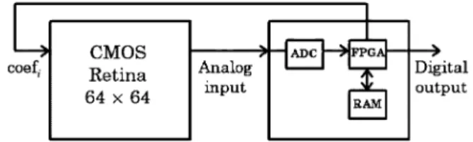
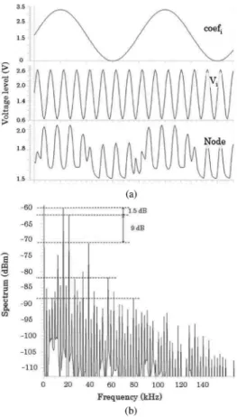
Half of the conversion time (200 ns) is used to perform the auto- zero operation. The other half is dedicated to the comparison. The working frequency of the counter is thus 2.4

Pour réduire l'affichage d'une image - cliquer sur l'icône zoom arrière dans la barre d'outils.. - cliquer sur le menu [Affichage >

Further works will concern on the one hand the generalization of electronic front propagation ma- nipulation (how to determine B is the key point) in order to expand the field

Avec ses 8000 membres répartis dans trente-neuf cercles fribourgeois disséminés dans notre pays - pour la plus grande partie en Suisse romande - il était dif¬. ficile pour

Glycosyl hydrolase family 1 Amino acid tRNA synthetase class I E and Q Homologous to ATPase AAA family Unknown function PPR repeats Homologous to calcineurin B Homologous

Copyright and moral rights for the publications made accessible in the public portal are retained by the authors and/or other copyright owners and it is a condition of

Based on the HA substitution rate in the SO farm (subline- age B), it would have taken a minimum of 18 weeks for the south-west Nigerian strains (sublineages A and B) to evolve from

-Teneurs sériques moyennes en créatinine chez les patients atteints l’IRC et diabétiques avant et après de traités par hémodialyse (HD). Les valeurs moyennes de la créatinine