Contributed Review: Experimental characterization of inverse
piezoelectric strain in GaN HEMTs via micro-Raman spectroscopy
The MIT Faculty has made this article openly available. Please share
how this access benefits you. Your story matters.
Citation Bagnall, Kevin R. and Wang, Evelyn N. “Contributed Review: Experimental Characterization of Inverse Piezoelectric Strain in GaN HEMTs via Micro-Raman Spectroscopy.” Review of Scientific Instruments 87, 061501 (June 2016): 1-22
As Published http://dx.doi.org/10.1063/1.4954203
Publisher American Institute of Physics (AIP)
Version Author's final manuscript
Citable link http://hdl.handle.net/1721.1/110369
Terms of Use Creative Commons Attribution-Noncommercial-Share Alike
1
Experimental characterization of inverse piezoelectric strain in GaN HEMTs
via micro-Raman spectroscopy
Kevin R. Bagnall and Evelyn N. Wang
Department of Mechanical Engineering, Massachusetts Institute of Technology, Cambridge, Massachusetts, 02139, USA
Micro-Raman thermography is one of the most popular techniques for measuring local temperature rise in gallium nitride (GaN) high electron mobility transistors (HEMTs) with high spatial and temporal resolution. However, accurate temperature measurements based on changes in the Stokes peak positions of the GaN epitaxial layers requires properly accounting for the stress and/or strain induced by the inverse piezoelectric effect. It is common practice to use the pinched OFF state as the unpowered reference for temperature measurements because the vertical electric field in the GaN buffer that induces inverse piezoelectric stress/strain is relatively independent of the gate bias. Although this approach has yielded temperature measurements that agree with those derived from the Stokes/anti-Stokes ratio and thermal models, there has been significant difficulty in quantifying the mechanical state of the GaN buffer in the pinched OFF state from changes in the Raman spectra. In this paper, we review the experimental technique of micro-Raman thermography and derive expressions for the detailed dependence of the Raman peak positions on strain, stress, and electric field components in wurtzite GaN. We also use a combination of semiconductor device modeling and electro-mechanical modeling to predict the stress and strain induced by the inverse piezoelectric effect. Based on the insights gained from our electro-mechanical model and the best values of material properties in the literature, we analyze changes in the E2 high and A1 (LO) Raman peaks and demonstrate that there are major quantitative
discrepancies between measured and modeled values of inverse piezoelectric stress and strain. We examine many of the hypotheses offered in the literature for these discrepancies but conclude that
2
none of them satisfactorily resolves these discrepancies. Further research is needed to determine whether the electric field along the 𝑐-axis could be affecting the phonon frequencies apart from the inverse piezoelectric effect in wurtzite GaN, which has been predicted theoretically in zinc blende gallium arsenide (GaAs).
I. Introduction
Due to the excellent electrical properties of gallium nitride (GaN), GaN-based high electron mobility transistors (HEMTs) are one most promising semiconductor technologies for high power, high frequency defense and commercial wireless communications applications [1]. However, the high dissipated power densities present in GaN power amplifiers (PAs) can lead to high channel temperatures and degraded performance and reliability. Over the last ten years, micro-Raman spectroscopy has become one of the most popular techniques for measuring local temperature rise in GaN HEMTs owing to its high spatial resolution of ≈1 µm and the wide availability of commercial micro-Raman systems [2]-[9]. The temperature of the GaN epitaxial layer(s) of interest is typically measured by either the change in center position or linewidth of the Stokes peak or the ratio of the intensities of the Stokes to anti-Stokes peaks. Although the Stokes/anti-Stokes ratio technique is theoretically more ideal for temperature measurements because it is not affected by mechanical stress or strain, the Stokes peak position technique is more popular because of the longer acquisition time and more expensive optical filters required for Stokes/anti-Stokes measurements [4],[9]. It has also been suggested that the non-equilibrium distribution of hot phonons emitted by electron-phonon scattering in GaN HEMTs could lead to erroneous temperature measurements using the Stokes/anti-Stokes ratio of the A1 (LO) mode [10].
3
The earliest reports of micro-Raman thermography in GaN HEMTs utilized an empirical formula fitted to experimental data to relate the Stokes line position to the GaN temperature [2],[11]. Over time, it has been recognized that the inverse piezoelectric (IPE) and thermoelastic effects may also change the Stokes line position when a GaN HEMT is biased in the ON state, which needs to be accounted for in order to accurately measure the device temperature [4],[7]-[9],[12]. Sarua et al. (2006) first reported that the E2 high and A1 (LO) peak positions change with
increasing drain bias in the pinched OFF state relative to the zero bias state despite the negligible temperature rise associated with near zero dissipated power [12]. The authors attributed the change in Stokes peak positions to stress and strain induced by the inverse or converse piezoelectric effect but observed an order of magnitude disagreement between the values of stress and strain derived from micro-Raman measurements and those predicted by electrical device modeling. Sarua et al. (2006) also suggested that the pinched OFF state with the same drain bias as the ON state should be used as the reference for temperature measurements based on the change in Stokes peak position rather than the zero bias state. Subsequent reports have confirmed that measuring the changes in Stokes peak position and/or linewidth with the pinched OFF state as a reference results in temperature values in good agreement with Stokes/anti-Stokes and thermomechanical modeling [7]-[9]. However, a clear, quantitative description of the electro-mechanical state of the GaN layer(s) in the pinched OFF state has remained elusive [13]-[14].
In this paper, we review the previous work on experimental characterization of IPE stress and strain in GaN HEMTs via micro-Raman spectroscopy in an effort to better understand the use of the pinched OFF state as a reference for temperature measurements. First, we describe the experimental technique and discuss popular methods for extracting the GaN temperature rise from changes in the Stokes peak positions. We perform electrical device modeling of a GaN HEMT and
4
uncoupled electro-mechanical modeling of the GaN buffer to clarify the mechanism of IPE stress and strain in the GaN buffer and to examine how mechanical boundary conditions affect the depth-averaged values of these quantities. Next, we review the relevant material properties used to relate changes in Stokes peak positions to stress and strain and suggest that uncertainty in the values of these material properties does not explain the discrepancy between the measured and predicted values of stress and strain. We analyze published experimental data on the changes in Stokes peak positions and show that extracted values of the stress and strain do not agree in sign and/or order of magnitude with predicted values from electrical and electro-mechanical modeling, depending upon which Raman peaks are considered in the analysis. In particular, we find that several hypotheses offered in the literature for these discrepancies, including (i) uncertainties in the material properties, (ii) non-classical piezoelectric coupling, and (iii) correlation between the peak electric field and depth-averaged stress, are not supported by our model and the published experimental data. Finally, we suggest that the electric field in the pinched OFF state could strongly affect the Stokes peak position apart from the IPE-induced strain and highlight several open questions in the field.
II. Experimental Technique
A. Micro-Raman SpectroscopyRaman spectroscopy is one of the most common experimental techniques for identifying materials and characterizing their structure, quality, temperature and other properties by measuring the frequencies of their vibrational modes [15], particularly for III-nitride semiconductors [16]. In the Raman scattering process, an incident photon with wavelength 𝜆0 is scattered to a wavelength
5
𝜆 by emitting (Stokes process) or absorbing (anti-Stokes process) a phonon. The relative change in wavenumber of a photon before and after a Raman scattering event
𝜔 = 1 𝜆0−
1
𝜆 (1)
is directly proportional to the frequency of the phonon emitted or absorbed in the Raman scattering process and is thus a measure of the phonon frequency. Due to the fact that photons carry a significant amount of energy but little momentum and phonons have relatively low energies but large momenta, Raman scattering in semiconductors generates and absorbs only optical phonons near the center of the first Brillouin zone (Γ-point). Momentum conservation and crystal symmetry considerations place further constraints on the optical phonon modes that may be observed for a given scattering configuration, i.e., the incoming and scattered photon directions relative to the crystallographic orientation, which lead to selection rules. In this work, we mainly discuss the Stokes process associated with optical phonon emission and use the terms “Stokes peak position,” “Raman peak position,” and “phonon frequency” interchangeably as they refer to quantities that are directly proportional to each other.
Micro-Raman spectroscopy specifically involves the focusing of the laser excitation to a micron size spot on the sample whose diameter and collection depth are limited by the diffraction of light. Notch or edge filters are needed to block the Rayleigh scattered light at the excitation wavelength 𝜆0, and the Raman scattered light is dispersed into a spectrum with a spectrometer or monochromator. A phonon mode generated by Raman scattering appears as a peak with a center position corresponding to the phonon frequency and a finite linewidth associated with the phonon lifetime and instrumental response, i.e., the point spread function, of the spectrometer [17]. The precision with which a change in the Raman peak position can be measured depends on the optical
6
characteristics of the spectrometer (grating groove density, focal length, and slit width), pixel size of the detector, and features of the Raman peak (intensity, linewidth, and proximity to other peaks). The highest precision is achieved by fitting a Raman peak with a lineshape, such as a Lorentzian, Gaussian, or Voigt profile, to determine the center of the peak for each measurement [18]. Uncertainties in the change in Raman peak position as small as 0.01 cm-1 based on the random error of repeated measurements are possible with commercially-available micro-Raman systems, frequency-stabilized laser sources, and careful spectrometer calibration.
B. GaN High Electron Mobility Transistors
GaN-based transistors have attracted significant interest in recent years due to the material’s wide bandgap, high critical electric field, and potential to develop a variety of heterostructures with epitaxial layers of alloys of other III-nitride semiconductors [19]. In particular, the AlGaN/GaN heterostructure results in a high density two-dimensional electron gas (2DEG) due to a difference in spontaneous and piezoelectric polarization between the two materials [20]. The unique combination of high electron concentration and mobility of the 2DEG and high critical electric field of AlGaN and GaN layers simultaneously allows for high operating voltages and current densities in the lateral HEMT structure. Thus, GaN HEMTs can operate at significantly higher power densities for radio-frequency (RF) and microwave power amplifier (PA) applications than other semiconductor devices, such as those based on gallium arsenide [1],[21]. GaN HEMTs also exhibit excellent performance at high switching frequencies and efficiency savings in power conversion applications because of their low on-resistances and high breakdown voltages [22].
7
Due to the challenges in growing bulk GaN substrates in large sizes and with low defect densities, GaN is typically grown on a foreign substrate, such as sapphire, silicon carbide (SiC), or silicon. For high performance GaN PAs with significant power dissipation, SiC is preferred as a substrate because of its high thermal conductivity (420 K) compared to silicon (150 W/m-K) and sapphire (35 W/m-W/m-K) [5]. Both GaN and SiC (4H-SiC and 6H-SiC) are wurtzite crystals belonging to the point group 𝐶6𝑣 with a hexagonal Bravais lattice. In the epitaxy process, typically
1 to 2 µm of GaN is grown on the (0001) plane (𝑐-plane) of SiC after AlN and/or AlGaN nucleation and stress management layers are deposited so that the [0001] direction or 𝑐-axis of GaN and SiC are aligned. A much thinner AlGaN barrier of 15 to 30 nm is grown on the top of the GaN buffer to form the heterojunction and 2DEG. Transistors are fabricated on AlGaN/GaN heterostructures by forming ohmic contacts for the source and drain and a Schottky or metal-insulator-semiconductor contact for the gate. Schematics of the wurtzite GaN unit cell, crystal structure, and basic HEMT structure are shown in Figure 1. The difference in lattice constants and coefficient of thermal expansion between the epitaxial layers results in residual stress/strain in the GaN buffer and AlGaN barrier when the wafer is cooled to room temperature. For other substrates, thicker GaN epilayers and/or more complex nucleation and stress management layers may be needed to provide the desired electrical properties of the buffer and prevent cracking [24].
8
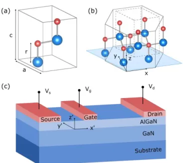
FIG. 1. (a) Wurtzite GaN unit cell, (b) crystal structure, and (c) basic GaN HEMT structure. Larger blue and smaller red spheres denote Ga and N ions, respectively. Crystal structures were
drawn with the VESTA visualization software [23]. The drain and gate biases are referenced with respect to the source, i.e., 𝑉𝑑𝑠 = 𝑉𝑑− 𝑉𝑠 and 𝑉𝑔𝑠 = 𝑉𝑔− 𝑉𝑠.
The hexagonal lattice structure of wurtzite GaN depicted in Figure 1 (a) and (b) is described by two lattice parameters, 𝑎 and 𝑐, and a third internal structural 𝑟 parameter denoting the distance between the Ga and N atoms or bond length along the 𝑐-axis. In the Miller-Bravais index system (ℎ𝑘𝑖ℓ) [25], the 𝑥-axis of the hexagonal crystal structure is chosen to be the [11-20] direction, and the 𝑧-axis set equal to the 𝑐-axis or [0001] direction [26]-[27]. In order to form a mutually orthogonal, right-handed coordinate system, the 𝑦-axis is then chosen to be the [-1100] direction. This crystallographic coordinate system is used to define the tensor components of the material properties of wurtzite GaN, which must be invariant under the symmetry operations of the point group 𝐶6𝑣. However, there is also the need to define a convenient coordinate system 𝑥′,𝑦′,𝑧′ with respect to the features of a lateral GaN HEMT, such as the channel and gate contact. As mentioned previously, GaN epilayers grown on SiC substrates have the 𝑐-axis of the two materials aligned so it is natural to choose the 𝑧′-axis of the transistor to be the same as the 𝑧-axis of the crystal.
9
Following previous works [12], we chose the 𝑥′- and 𝑦′-axes to correspond to the directions perpendicular to and along the gate, respectively, as shown in Figure 1 (c). Depending on how a transistor is fabricated with respect to the crystallographic planes, there is the possibility of a difference in angle 𝜃 of rotation between the 𝑥- and 𝑥′-axes of the crystallographic and transistor coordinate systems, respectively. We address this issue and its implications in detail in Section II. C. and Appendix A, showing that it does not affect the interpretation of changes in micro-Raman spectra related to IPE-induced stress and strain.
Raman spectra from GaN HEMTs are typically measured in the 𝑧̅(∙∙)𝑧 backscattering configuration, in which the laser excitation is directed along the [000-1] direction of wurtzite GaN by a microscope objective and the Raman scattered light is collected by the same objective along the reverse path. Raman selection rules specify that only three of the nine possible optical phonon modes, assigned the labels E2 high, E2 low, and A1 (LO) from group theory, are accessible in the
𝑧̅(∙∙)𝑧 backscattering scattering configuration in wurtzite GaN [28]. While the E2 modes are
observable with the polarization of the laser parallel, i.e., 𝑧̅(𝑥𝑥)𝑧 or 𝑧̅(𝑦𝑦)𝑧, and perpendicular, i.e., 𝑧̅(𝑥𝑦)𝑧 or 𝑧̅(𝑦𝑧)𝑧, to that of the collection optics, the A1 (LO) mode is only observable in the
parallel polarization configuration. Measurements of the E2 high mode are most common due its
high intensity for samples of good crystal quality. Characterization of the A1 (LO) mode is also
common although it is broader and less intense than the E2 high mode. The E2 low mode is rarely
reported in the literature due to its low frequency (140 to 145 cm-1), low intensity, and very narrow linewidth, making it difficult to measure except with high resolution spectrographs and optical filters with very sharp transitions near the laser wavelength. In most studies, microscope objectives of 50× to 100× magnification with numerical apertures (NA) of 0.5 to 0.6 result in a laser spot size of ≈1 to 1.3 µm [4],[9]. Objectives with higher NA values and smaller associated laser spot
10
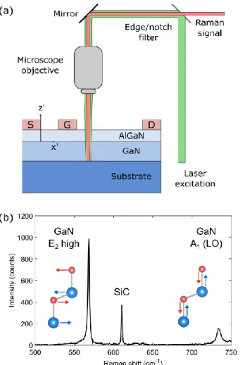
sizes are widely available but difficult to use with on-wafer devices due to the need for a substantial working distance to accommodate electrical probes. The depth of field, also determined by the laser wavelength and NA and magnification of the objective, is often ≈1 to 3 µm, depending upon the confocal pinhole size if present [4],[29]. These considerations with respect to focusing of the laser and collection of scattered light by the objective mean that the Raman spectrum is collected from a volume extending throughout the depth of the GaN epitaxial layer(s) (1 to 2 µm) with a diameter of ≈1 µm. Thus, temperature, stress, and strain values extracted from micro-Raman spectroscopy represent area- and depth-averaged values of these quantities, which may vary significantly within the excitation/collection volume both laterally and across the GaN layer(s). A schematic of micro-Raman spectroscopy of GaN HEMTs is shown in Figure 2 with a sample spectrum of a GaN epilayer structure on 4H-SiC.
11
FIG. 2. (a) Schematic of micro-Raman spectroscopy technique on GaN HEMTs and (b) sample spectrum of a GaN on 4H-SiC substrate with 532 nm laser excitation with phonon modes
depicted in the inset. The schematic in (a) is not drawn to scale.
C. Micro-Raman Thermometry in GaN HEMTs
Although commercially-available, high resolution spectrometers are capable of measuring Stokes peak position changes as small as 0.01 cm-1 by fitting a lineshape (typically a Voigt profile) to the Raman peaks of GaN, the accuracy with which temperature can be measured also depends on the accuracy of the relationship between temperature and peak position determined by calibration. Empirical relations for the dependence of the Stokes peak position on temperature have been proposed in the GaN literature, such as
12
𝜔(𝑇) = 𝜔0− 𝐴
exp(𝐵ℏ𝜔0/𝑘𝐵𝑇) − 1 (2)
where 𝜔(𝑇) is the Stokes line position, 𝑇 is the absolute temperature, 𝜔0 is the Stokes line position
at absolute zero temperature, and 𝐴 and 𝐵 are fitting constants determined by calibration [11],[30]. However, this relation is not rigorously derived from crystal lattice dynamics and does not provide a physical explanation for the reason GaN free standing and epitaxial films have different values of the parameters 𝜔0, 𝐴, and 𝐵. In contrast, a clear relationship between the optical phonon frequency and temperature has been derived from a quantum mechanical treatment of crystal lattice dynamics including anharmonic effects
∆𝜔 = 𝜔(𝑇) − 𝜔(𝑇0) = ∆𝜔𝑠𝑡𝑟𝑎𝑖𝑛+ ∆𝜔𝑑𝑒𝑐𝑎𝑦 (3)
where ∆𝜔 is the change in total change in phonon frequency due to a change in temperature from a reference state at temperature 𝑇0 and ∆𝜔𝑠𝑡𝑟𝑎𝑖𝑛 and ∆𝜔𝑑𝑒𝑐𝑎𝑦 are the contributions from thermal
expansion and phonon-phonon interactions, respectively [31]-[32]. While discussion of the exact expression for ∆𝜔𝑑𝑒𝑐𝑎𝑦 is beyond the scope of this paper, Equation (3) is particularly useful in understanding the mechanisms responsible for phonon frequency shift with temperature. Thermal expansion results in strain, which changes the interatomic potential between atoms and force constants, and a change in temperature also affects the phonon-phonon scattering processes by changing the phonon occupation probability. Thus, Equation (3) applies to GaN epitaxial layers, free standing films, and bulk substrates. The phonon frequency shift due to thermal expansion Δ𝜔𝑠𝑡𝑟𝑎𝑖𝑛 is different for each kind of GaN sample because the mechanical constraints on a sample
determine the amount of thermal strain for a given temperature rise. In contrast, the phonon frequency shift associated with phonon-phonon interactions Δ𝜔𝑑𝑒𝑐𝑎𝑦 should only depend on the
13
intrinsic properties of GaN and should be relatively sample-independent. It is immediately evident that any other crystal effect that induces strain, such as the IPE effect, could shift the phonon frequency in addition to thermal expansion. Although the ∆𝜔𝑑𝑒𝑐𝑎𝑦 contribution to the phonon frequency shift varies nonlinearly with absolute temperature, it has been observed that the change in phonon frequency with temperature is approximately linear with temperature from 25 °C to 300 °C for both GaN epitaxial films on SiC substrates and bulk GaN samples [8]-[9].
Understanding the strain contribution to the phonon frequency shift Δ𝜔𝑠𝑡𝑟𝑎𝑖𝑛 of the GaN buffer in a HEMT requires a detailed analysis of the piezoelectric and thermoelastic contributions to the strain for a given bias condition. When a GaN HEMT is biased in the ON state, i.e., 𝑉𝑑𝑠 =
𝑉𝑑− 𝑉𝑠 > 0 and 𝑉𝑔𝑠 = 𝑉𝑔− 𝑉𝑠 > 𝑉𝑡ℎ, where 𝑉𝑑, 𝑉𝑠, and 𝑉𝑔 are the voltages of the drain, source,
and gate contacts, respectively, and 𝑉𝑡ℎ is the gate threshold voltage, there is an increase in temperature due to Joule heating and an electric field due relative to the zero bias state (𝑉𝑑𝑠 = 0
and 𝑉𝑔𝑠 = 0). Because GaN is a piezoelectric, thermoelastic solid, the strain components at each
point in the material are related to the stress, electric field, and temperature rise through the constitutive relation
𝜖𝑖 = 𝑠𝑖𝑗𝜎𝑗+ 𝛼𝑖∆𝑇 + 𝑑𝑘𝑖𝐸𝑘 (4)
where 𝜖𝑖 is the strain vector written in contracted notation, 𝜎𝑗 is the stress vector, 𝐸𝑘 is the electric field, 𝑠𝑖𝑗 is the elastic susceptibility tensor, 𝛼𝑖 are the coefficients of thermal expansion, and 𝑑𝑘𝑖
are the piezoelectric moduli [25]. Under the continuum approximation, the strain tensor at each infinitesimal point 𝑥, 𝑦, 𝑧 is defined by the gradient in the displacement vector 𝑢⃗
𝜖𝑖𝑗 =1 2( 𝜕𝑢𝑖 𝜕𝑥𝑗 + 𝜕𝑢𝑗 𝜕𝑥𝑖) (5)
14
where 𝑥 = 𝑥𝑒̂1+ 𝑦𝑒̂2+ 𝑧𝑒̂3 is the position vector [34]. From the perspective of the crystal lattice,
the strain components are related to the change in lattice parameters 𝜖𝑥𝑥 = 𝜖𝑦𝑦 =𝑎 − 𝑎0
𝑎0 (6a)
𝜖𝑧𝑧= 𝑐 − 𝑐0
𝑐0 (6b)
where 𝑎0 and 𝑐0 are the unstrained lattice parameters if the normal strain is symmetric in the 𝑐-plane (𝜖𝑥𝑥 = 𝜖𝑦𝑦) [20]. If the strain is asymmetric in the 𝑐-plane (𝜖𝑥𝑥 ≠ 𝜖𝑦𝑦) or contains non-zero
shear strain components, the symmetry of the point group 𝐶6𝑣 is broken and the wurtzite crystal
can no longer be described by the lattice parameters 𝑎 and 𝑐, which leads to expressions more complicated than Equations (6a) and (6b).
Linear potential deformation theory predicts that Δ𝜔𝑠𝑡𝑟𝑎𝑖𝑛 for each phonon mode should
be governed by the symmetry of the mode and that of the perturbation to the crystal potential 𝑉𝑖𝑗′ associated with the strain tensor 𝜖𝑖𝑗. For phonon modes belonging to the E2 and A1 representations
in the point group 𝐶6𝑣, this relationship is given by the equations ∆𝜔𝐸2 = 𝑎𝐸2(𝜖𝑥𝑥+ 𝜖𝑦𝑦) + 𝑏𝐸2𝜖𝑧𝑧± 𝑐𝐸2√(𝜖𝑥𝑥− 𝜖𝑦𝑦)
2
+ 4𝜖𝑥𝑦2 (7a)
∆𝜔𝐴1 = 𝑎𝐴1(𝜖𝑥𝑥+ 𝜖𝑦𝑦) + 𝑏𝐴1𝜖𝑧𝑧 (7b)
where 𝑎, 𝑏, and 𝑐 are the strain phonon deformation potentials (PDPs) [33]. As noted in Section II. B., the crystallographic 𝑥,𝑦,𝑧 coordinate system for which the strain components in Equations (7a) and (7b) are defined may differ from the transistor 𝑥′,𝑦′,𝑧′ coordinate system by a rotation angle 𝜃 around the 𝑧 = 𝑧′ axis. However, we show in Appendix A that the quantities 𝜖𝑥𝑥+ 𝜖𝑦𝑦,
15
𝜖𝑧𝑧, and (𝜖𝑥𝑥− 𝜖𝑦𝑦)2+ 4𝜖𝑥𝑦2 are invariant under rotation around the 𝑧-axis so that Equations (7a)
and (7b) are equally valid in the transistor 𝑥′,𝑦′,𝑧′ coordinate system. For the remainder of this paper, we drop the prime notation and use 𝑥,𝑦,𝑧 to refer to the transistor coordinate system for convenience and without loss of generality.
As will be discussed in greater detail in Section III. A., the application of a positive drain bias results in a vertical electric field 𝐸𝑧 along the 𝑐-axis in the GaN buffer, which is only related
to the normal strains 𝜖𝑥𝑥, 𝜖𝑦𝑦, and 𝜖𝑧𝑧 through the piezoelectric modulus tensor components 𝑑31 =
𝑑32 and 𝑑33 [13],[25]. The electric field components in the 𝑐-plane 𝐸𝑥 and 𝐸𝑦 are coupled to the shear strain components 𝜖𝑥𝑧 and 𝜖𝑦𝑧, respectively. However, there is no dependence of the E2 high
and A1 (LO) frequencies on 𝜖𝑥𝑧 and 𝜖𝑦𝑧 in Equations (7a) and (7b), indicating that these
components do not result in changes in the Raman peak positions observed in the backscattering configuration. The detailed form of the strain contribution to the E2 high peak position in terms of
the stress, temperature rise, and electric field components can be derived by inserting Equation (4) into Equation (7a)
∆𝜔𝐸2 = [𝑎𝐸2(𝑠11+ 𝑠12) + 𝑏𝐸2𝑠13](𝜎𝑥𝑥+ 𝜎𝑦𝑦) + [2𝑎𝐸2𝑠13+ 𝑏𝐸2𝑠33]𝜎𝑧𝑧 ± 𝑐𝐸2|𝑠11− 𝑠12|√(𝜎𝑥𝑥 − 𝜎𝑦𝑦)2 + 4𝜎𝑥𝑦2 + [2𝑎
𝐸2𝑑31+ 𝑏𝐸2𝑑33]𝐸𝑧 + [2𝑎𝐸2𝛼𝑥𝑥+ 𝑏𝐸2𝛼𝑧𝑧]Δ𝑇
(8)
where we have used the identity 𝑠66 =12(𝑠11− 𝑠12) for the point group 𝐶6𝑣 [25]. The dependence
of the A1 (LO) peak position on these quantities is the same as Equation (8) with the exception of
the third term associated with the asymmetric normal stress and shear stress in the 𝑥𝑦-plane, which is omitted for the A1 (LO) mode. The dependence of the E2 high peak shift in Equation (8) contains
16
six unknown variables (𝜎𝑥𝑥, 𝜎𝑦𝑦, 𝜎𝑧𝑧, 𝜎𝑥𝑦, 𝐸𝑧 and Δ𝑇) that could all simultaneously be affecting
the E2 high peak position under an arbitrary gate and drain bias applied to a GaN HEMT. These
six unknown variables can be reduced to only three by evaluating the relative magnitudes of various terms in Equation (8).
Provided the GaN buffer behaves as a linear piezoelectric material, there should be negligible shear stress in the 𝑐-plane (𝜎𝑥𝑦≈ 0) except for near the edges of the die [7]. In most
experiments, the top surface of the GaN buffer is free to move because there is nothing to prevent it from expanding or contracting, leading to negligible stress along the 𝑐-axis (𝜎𝑧𝑧 ≈ 0) [9]. Although the piezoelectric moduli 𝑑31 and 𝑑32 are equal, the normal strain and stress components
in the 𝑐-plane are also determined by the spatial variation of the vertical electric field 𝐸𝑧(𝑥, 𝑦) and
the mechanical boundary conditions imposed on the GaN buffer. Because of the inherent asymmetry of the lateral HEMT structure, the 𝐸𝑧 electric field component varies significantly in
the 𝑥-direction (along the channel) but is almost constant in the 𝑦-direction (parallel to the gate). Thus, one would expect that the strain and stress components in these two directions should not be equal (𝜖𝑥𝑥 ≠ 𝜖𝑦𝑦 and 𝜎𝑥𝑥 ≠ 𝜎𝑦𝑦). According to Equation (8), asymmetry of the normal stress components in the 𝑐-plane would result in a splitting of the Raman peak position of the E2 high
mode between Raman spectra acquired in the parallel and cross-polarized configurations [27]. Previous measurements of GaN HEMTs biased in the pinched OFF state have reported that this splitting of the E2 high mode is not detectable within experimental uncertainty [13]. This suggests
that the asymmetry in the in-plane strain 𝜖𝑥𝑥− 𝜖𝑦𝑦 and in-plane stress 𝜎𝑥𝑥− 𝜎𝑦𝑦 is small
compared to the values of the strain and stress components themselves. The assumption of symmetric IPE-induced strain and stress in the 𝑐-plane (𝜖𝑥𝑥 ≈ 𝜖𝑦𝑦 and 𝜎𝑥𝑥 ≈ 𝜎𝑦𝑦) is then a good
17
approximation that allows one to further simplify Equation (8). Our 3D electro-mechanical model of the GaN buffer discussed in Section III. B. also suggests that the stress is approximately biaxial. Taking of all of these simplifications into account, the change in Stokes peak position of the E2 high and A1 (LO) modes between the ON state and the zero bias state can be expressed as
∆𝜔 = 𝜔𝑂𝑁− 𝜔0 = 𝐾𝐼𝐼𝜎𝑥𝑥+ 𝐴∆𝑇 + 𝐵𝐸𝑧 (9)
where 𝜔𝑂𝑁 and 𝜔0 are the Stokes line positions of the ON state and zero bias state, respectively,
𝐾𝐼𝐼 is the biaxial stress coefficient, 𝐴 is the linear temperature coefficient, and 𝐵 is the electric
field coefficient. One should note that the values of stress, temperature difference, and electric field in Equation (9) are the differences in these quantities between the ON state and zero bias state, not absolute values of these quantities. In addition, the derivation of Equation (9) does not assume that the strains in the 𝑐-plane 𝜖𝑥𝑥 and 𝜖𝑦𝑦 are zero. The biaxial stress appearing in Equation (9) for an ON state bias is a combination of the biaxial stresses due to the IPE and thermoelastic effects. The biaxial stress coefficient 𝐾𝐼𝐼 and IPE-related electric field coefficient 𝐵 under these
assumptions are given by
𝐾𝑛𝐼𝐼 = 2𝑎𝑛(𝑠11+ 𝑠12) + 2𝑏𝑛𝑠13 (10a)
𝐵𝑛 = 2𝑎𝑛𝑑13+ 𝑏𝑛𝑑33 (10b)
which have different values for the E2 high and A1 (LO) modes due to different values of the strain
PDPs. The first term involving the strain PDP 𝑎 is related to the in-plane strain components while the second term with 𝑏 is related to the out-of-plane strain component.
If change in the Stokes peak position of only one phonon mode, such as the E2 high mode,
is measured from the zero bias state to the ON state, the temperature rise cannot be properly decoupled from the stress and electric field. Simultaneous measurement of two phonon modes,
18
usually the E2 high and A1 (LO), still cannot successfully isolate the temperature rise because there
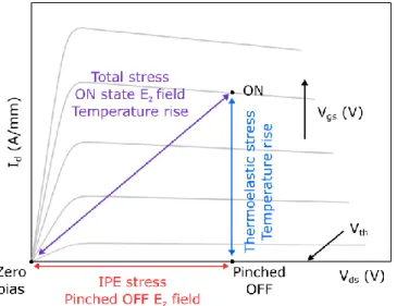
are two equations of the form of Equation (9) and three unknowns (𝜎𝑥𝑥, ∆𝑇, and 𝐸𝑧). Sarua et al. (2006) was the first to suggest that the pinched OFF state (𝑉𝑑𝑠 > 0 and 𝑉𝑔𝑠 < 𝑉𝑡ℎ) at the same drain bias as the ON state should be used as the reference for temperature measurements rather than the zero bias state [12]. In the pinched OFF state, there is negligible current in the HEMT channel and negligible power dissipation, resulting in near zero temperature rise and thermoelastic stress. A schematic of the proposed measurement in the context of the drain current-drain voltage output characteristics (𝐼𝑑-𝑉𝑑𝑠) is shown in Figure 3.
FIG. 3. Schematic representation of the contributions of stress, temperature rise, and electric field to Stokes peak position between different HEMT bias points in the drain current-drain voltage (𝐼𝑑-𝑉𝑑𝑠) output characteristics. The gate threshold voltage 𝑉𝑡ℎ is the gate bias below
which there is negligible drain current (≲1 mA/mm).
The hypothesis that the difference in Stokes peak positions between the pinched OFF state and the zero bias state accounts for the IPE-induced stress and vertical electric field can only be true if the electric field in the pinched OFF state and the ON state is the same. In their seminal paper on this topic, Sarua et al. (2006) performed electrical device modeling and found this to be
19
approximately true [12]. Then, the contributions of the IPE effect and temperature rise can be written in terms of the difference in Raman peak positions between the ON state and the pinched OFF state ∆𝜔𝑂𝑁/𝑂𝐹𝐹 and the pinched OFF state and the zero bias state ∆𝜔𝑂𝐹𝐹/0
∆𝜔𝑂𝑁/𝑂𝐹𝐹 = 𝜔𝑂𝑁− 𝜔𝑂𝐹𝐹 = 𝐾𝐼𝐼𝜎
𝑥𝑥𝑇𝐸+ 𝐴∆𝑇 (11a)
∆𝜔𝑂𝐹𝐹/0 = 𝜔𝑂𝐹𝐹− 𝜔0 = 𝐾𝐼𝐼𝜎𝑥𝑥𝐼𝑃𝐸+ 𝐵𝐸𝑧 (11b)
where 𝜎𝑥𝑥𝐼𝑃𝐸 and 𝜎
𝑥𝑥𝑇𝐸 are the stresses due to the IPE and thermoelastic effects, respectively. A more
rigorous justification of Equations (11a) and (11b) and the conditions for which they apply are provided in Appendix B. Since the introduction of the pinched OFF state as the proper reference for micro-Raman thermography, temperature measurements of the ON state based on the Stokes peak position and linewidth have shown good agreement with Stokes/anti-Stokes measurements and thermal models [7]-[9]. Thus, it is widely accepted in the GaN electronics community that using the pinched OFF state properly accounts for the stress and/or strain induced by the IPE effect.
D. IPE Stress and Strain Measurement
Despite the importance of accounting for the contribution of the electric field and the IPE-induced stress and popularity of using the pinched OFF state as the reference, relatively few papers have attempted to quantify the electric field magnitude and IPE stress/strain in the pinched OFF state. Assuming the average vertical electric field across the GaN buffer to be the same in the ON state and pinched OFF state at the same drain bias, the change in Stokes peak position between the pinched OFF and the zero bias states should provide a self-consistent measurement of the induced IPE stress and vertical electric field according to Equation (11b). However, because Equation (11b) involves the two unknowns of stress 𝜎𝑥𝑥𝐼𝑃𝐸 and vertical electric field 𝐸𝑧, measurement of the
20
experimental method described in the literature to characterize the induced stress and strain is to (i) measure the Raman spectrum of a GaN HEMT in the zero bias state at a particular location and (ii) measure the same location in the pinched OFF state [8],[12]-[14]. Under the assumption of negligible shear strain and symmetric normal strains in the 𝑐-plane described in Section II. C., the changes in the frequency of the E2 high and A1 (LO) modes may be related to the normal strain
components by the set of two equations [∆𝜔𝐸2 ∆𝜔𝐴1 ] = [2𝑎𝐸2 𝑏𝐸2 2𝑎𝐴1 𝑏𝐴1 ] [𝜖𝜖𝑥𝑥 𝑧𝑧] (12)
where ∆𝜔𝐸2 and ∆𝜔𝐴1 represent the change in frequency of the E2 high and A1 (LO) modes
between the pinched OFF state and zero bias state, respectively. Using the simplified form of the constitutive relation in Equation (4) and assuming 𝜎𝑥𝑥 = 𝜎𝑦𝑦, the normal strain components can
also be related to the in-plane stress and vertical electric field through the set of two equations [𝜖𝜖𝑥𝑥 𝑧𝑧] = [ 𝑠11+ 𝑠12 𝑑31 2𝑠13 𝑑33] [ 𝜎𝑥𝑥 𝐸𝑧] (13)
Equations (12) and (13) thus provide a self-consistent experimental method for characterizing the induced strain, stress, and vertical electric field when a GaN HEMT is pinched off based on measurements of changes in E2 high and A1 (LO) frequency with the drain bias.
Due to the fact that lateral HEMTs for high frequency applications have a limited breakdown voltage associated with their relatively small gate-drain spacing of 2 to 4 µm, Sarua et
al. (2010) introduced an alternate structure for characterizing IPE stress and strain [13]. The
authors utilized two ohmic contacts on a standard AlGaN/GaN heterostructure that were electrically isolated by etching through the 2DEG at the AlGaN/GaN interface as shown in Figure 5 in Ref. [13]. Voltage differences between the two pads were applied up to 150 V and the changes
21
in E2 high and A1 (LO) peak positions monitored near the edge of the positively biased pad (termed
the drain) where the peak vertical electric field was expected [13]. When measured on the same epitaxial structure as lateral HEMTs, this pair of mesa-isolated contact pads permits higher induced stress and strains for more comprehensive characterization.
III. Modeling
Due to the complexity of the electric field distribution in a GaN HEMT and tensor nature of the stress and strain fields, electrical and electro-mechanical device modeling can provide helpful insight to guide the interpretation of experimental data from micro-Raman spectroscopy. Because the work by Sarua et al. (2006) is essentially the basis for using the pinched OFF state as the reference in micro-Raman thermometry, it is critically important to understand the key physics of the vertical electric field in the GaN buffer and the strain and stress fields it induces. Toward this goal, we discuss electrical modeling with the semiconductor device modeling software Silvaco ATLAS/BLAZE but from a different perspective than that of Sarua et al. (2006). We complement this device model with an uncoupled electro-mechanical model in COMSOL Multiphysics to investigate the nature of the IPE-induced strain and stress in the GaN buffer. In contrast to previous works [12]-[14], we have predicted the stress and strain distributions from the electro-mechanical model and the appropriate boundary conditions on the surfaces of the GaN buffer in order to understand the impact of these boundary conditions on the depth-averaged values of stress and strain that are correlated to Raman peak shifts. Although we modeled a specific GaN HEMT with the same dimensions as that of Sarua et al. (2006) [12] in order to compare our model with their experimental data, the conclusions regarding the electric field, stress, and strain distributions in the channel are widely applicable to a variety of devices with different layouts.
22
A. Electrical Device Modeling
Because of the difference in bandgap, electron affinity, and doping level of the materials present in an AlGaN/GaN HEMT, there is essentially always a built-in potential across the GaN buffer and vertical electric field in the zero bias state. When a positive drain bias (𝑉𝑑𝑠 > 0) is applied in the OFF state (𝑉𝑔𝑠< 𝑉𝑡ℎ), the drain bias raises the electric potential at the top of the
GaN buffer with respect to the bottom of the buffer. This difference in potential results in an additional vertical electric field primarily in the gate-drain access region and under the drain contact along the 𝑐-axis [12]. By convention, the positive 𝑧-axis for the wurtzite system is chosen to coincide with the 𝑐-axis pointing from the substrate to the AlGaN barrier for Ga-face grown GaN epilayers [20]. Thus, the vertical electric field in the gate-drain access region induced by a positive drain bias must have a negative sign, i.e., point along the negative 𝑧-axis, to be consistent with the sign convention chosen for the piezoelectric constants. This point regarding the sign of the vertical electric field, although basic, is crucial to our understanding of the IPE-induced strain and stress. It was not explicitly stated in the original paper by Sarua et al. (2006) but later noted by Sarua et al. (2010) and may be a continued source of confusion regarding the expected sign of the stress and strain components. In this work, we focus our discussion on the vertical electric field component 𝐸𝑧 rather than the lateral components 𝐸𝑥 and 𝐸𝑦 because the changes in Stokes peak
positions for the E2 high and A1 (LO) modes are not coupled to the lateral electric field
components, as was discussed in Section II. B.
In order to model the electric field distribution in the GaN-on-SiC HEMT structure reported by Sarua et al. (2006), we developed an electrical device model with the Silvaco ATLAS/BLAZE software similar to the authors [12]. The thicknesses of the Al0.25Ga0.75N barrier and GaN buffer
23
were 30 nm and 1.2 µm, respectively. A 100 nm thick AlN nucleation layer was included between the GaN buffer and 4H-SiC substrate as is typical in GaN-on-SiC epitaxy. The gate length was 0.8 µm and the gate-drain and gate-source distances were 3.2 µm and 1.2 µm, respectively, based on Figure 2(a) in Ref. [12]. A positive sheet charge with a nominal concentration 1013 cm-2 was introduced at the AlGaN/GaN interface to account for polarization effects, resulting in a simulated threshold voltage of 𝑉𝑡ℎ ≈ -4.2 V. The unpowered OFF state and pinched OFF state were simulated
in this model at a gate bias of 𝑉𝑔𝑠 = -6 V for which the drain current is less than 1 µA/mm. Deep acceptor-type traps with a density of 3.0 × 1016 cm-3 were introduced into the GaN buffer to
account for impurities that result in a space charge region in the buffer when the drain contact is positively biased. For simplicity, self-heating effects were not included in the model as the impact of channel temperature on device characteristics was not the focus of this study.
While previous works have provided plots of the electric field distribution in the GaN buffer, we believe that the electric potential distribution can provide more intuitive physical insight in this situation. Assuming the collection volume in micro-Raman spectroscopy samples all of the Raman scattered light emitted from a ≈1 µm diameter spot through the thickness of the GaN buffer, the extracted values of strain, stress, and electric field according to Equations (7a) to (9) represent the depth-averaged values of these quantities. Although the constitutive relation expressed in Equation (4) applies only to an infinitesimal point 𝑥,𝑦,𝑧 in the GaN buffer, an identical equation for the depth-averaged quantities can be derived by applying the average value theorem to each term
24
where the quantity with the overbar 𝑢̅ =1𝐿∫ 𝑢(𝑧)𝑑𝑧−𝐿0 is the value averaged through the depth of the GaN buffer. This depth-averaged constitutive relation does assume, however, that the elastic susceptibility, coefficients of thermal expansion, and piezoelectric moduli are constant over the volume of interest. Noting that by definition the electric field is minus the gradient of the electric potential 𝐸⃗ = −∇𝜑, the average 𝑧-component of the electric field is given by
𝐸̅𝑧 = 1 𝐿∫ 𝐸𝑧(𝑧)𝑑𝑧 0 −𝐿 = 1 𝐿∫ − 𝜕𝜑 𝜕𝑧𝑑𝑧 0 −𝐿 = −𝜑(0) − 𝜑(−𝐿) 𝐿 (15)
where 𝐿 is the thickness of the buffer, which is exactly the difference in electrostatic potential across the GaN buffer divided by the thickness of the buffer with the proper sign. Therefore, it is easier to see by inspection how the average vertical electric field changes with the gate and drain bias from contour plots of the electric potential rather than the vertical component of the electric field. Finally, we note that the default sign convention assigned to the vertical axis in the Silvaco ATLAS/BLAZE software is opposite of the convention for the wurtzite system. Silvaco ATLAS/BLAZE chooses the positive 𝑧-axis to point from the top to the bottom of the GaN buffer when a GaN HEMT structure is modeled as in Sarua et al. (2006) [12] and this work. The electric potential for the GaN-on-SiC HEMT modeled in this work is shown in Figure 4 under four bias conditions: (a) the zero bias state 𝑉𝑑𝑠 = 0 V and 𝑉𝑔𝑠 = 0 V, (b) the unpowered OFF state 𝑉𝑑𝑠 = 0 V and 𝑉𝑔𝑠 = -6 V, (c) the ON state with 𝑉𝑑𝑠 = 20 V and 𝑉𝑔𝑠 = 0 V, and (d) the pinched OFF state with
25
FIG. 4. Electric potential distribution for the GaN HEMT structure reported in Ref. [12] for (a) the zero bias state 𝑉𝑑𝑠 = 0 V and 𝑉𝑔𝑠 = 0 V , (b) the unpowered OFF state 𝑉𝑑𝑠 = 0 V and 𝑉𝑔𝑠 = -6
V, (c) the ON state with 𝑉𝑑𝑠 = 20 V and 𝑉𝑔𝑠 = 0 V, and (d) the pinched OFF state with 𝑉𝑑𝑠 = 20
V and 𝑉𝑔𝑠 = -6 V.
When the device is in the zero bias state (all contacts grounded), there is a built-in potential of 3.4 V across the 1.2 µm thick GaN buffer due to the band alignment in equilibrium as shown in Figure 4(a). As a negative bias is applied to the gate while the drain and source are grounded, the 2DEG underneath the gate is depleted while the electric potential of the bulk of the buffer remains almost unchanged, which can be seen in the small difference between Figure 4(a) and (b). The application of a positive drain bias raises the electric potential at the top of the GaN buffer, inducing a potential difference across the buffer in most of the gate-drain access region and under the drain contact as seen in Figure 4(c) and (d). Meanwhile, the potential difference across the buffer in the source-gate access region and under the source contacts is virtually unchanged
26
because the source contact has electrostatic control over this region of the device. There is only a minor difference in the potential difference across the GaN buffer between the ON state and the pinched OFF state at 𝑉𝑑𝑠 = 20 V. The surface potential of the buffer in the ON state is slightly
lower than in the pinched OFF state because of the ohmic drop across the resistance gate-drain access region when there is significant current in the ON state. As first proposed by Sarua et al. (2006) [12], this behavior suggests that the pinched OFF state at a certain drain bias provides an accurate estimate of the IPE stress and strain present in the ON state at the same drain bias because the drain bias primarily determines the vertical electric field in the gate-drain access region and under the drain contact.
B. Electro-mechanical Modeling
As discussed in the previous section, the application of a positive drain bias in the pinched OFF state induces a difference in electric potential across the GaN buffer and vertical electric field predominately in the gate-drain access region of the channel and underneath the drain contact. This vertical electric field induces a combination of mechanical stress and strain according to the constitutive relation in Equation (4) such that the mechanical stress satisfies the static equilibrium condition
∇ ∙ 𝜎⃡ = 0 (16)
and any conditions on the stress or displacement components at the boundaries. Hence, the vertical electric field may be considered as the input needed to solve Equations (4) and (16) simultaneously for the stress and strain at each point in the HEMT structure. If the material properties and electrical behavior of a GaN HEMT are not significantly affected by the induced stress and strain, an uncoupled electro-mechanical model that calculates the stress and strain distributions from the
27
electric potential distribution provides a good approximation to the fully-coupled electro-mechanical problem. While a fully-coupled electro-electro-mechanical model of a GaN HEMT could be needed to assess the impact of the very high electric field (~1 MV/cm) near the gate contact on stress in the AlGaN buffer [35], the much smaller electric field, stress, and strain magnitudes in the GaN buffer can be predicted accurately with an uncoupled model.
Due to the complexity in solving this 3D electro-mechanical problem for the strain and stress distributions, several further simplifications have been made in the literature for GaN HEMTs. One of these simplifications is the 2D plane strain approximation [34]-[35], which assumes that the normal strain along the gate 𝜖𝑦𝑦 and the shear strain components 𝜖𝑥𝑦 and 𝜖𝑦𝑧 are
zero because the gate width of a lateral GaN HEMT is typically much longer than the channel length, and the vertical electric field distribution 𝐸𝑧(𝑥, 𝑧) is approximately the same for each plane
parallel to the 𝑥𝑧-plane within the active HEMT area. The GaN buffer is prevented from deforming in the 𝑦-direction because of the clamping by the buffer outside the active area (in which the vertical electric field is zero) and by the substrate underneath the buffer in the active area. As a result of this mechanical constraint in the 𝑦-direction, there must be a corresponding normal stress along the gate 𝜎𝑦𝑦 ≠ 0. Another assumption, which has been commonly used in interpreting
changes in micro-Raman spectra due to IPE-induces strain and stress, is that the GaN buffer is rigidly clamped in the 𝑐-plane by the substrate [12]-[14]. This implies that the bottom surface of the buffer has zero displacement under a vertical electric field 𝐸𝑧 of any magnitude. Due to the
high stiffness of wurtzite GaN, it also suggests that the normal strain components in the 𝑐-plane through the thickness of the buffer are approximately zero (𝜖𝑥𝑥 ≈ 0 and 𝜖𝑦𝑦 ≈ 0).
In this work, we developed a 3D uncoupled electro-mechanical model of the GaN buffer (1.2 µm), AlN nucleation layer (100 nm), and 4H-SiC substrate (100 µm) using the finite element
28
software COMSOL Multiphysics to calculate the stress and strain distributions due to the IPE effect [36]. In the 3D model, we included the nucleation layer and substrate to evaluate the impact of the finite stiffness of these layers on the in-plane strain components. We also calculated the stress and strain distributions for 2D models under the plane strain approximation in the 𝑥𝑧-plane with and without the AlN nucleation layer and SiC substrate to evaluate the impact of these approximations. In this section and throughout the remainder of the paper, we use the term “in-plane” to refer to the stress and strain components in the 𝑐-plane and “out-of-“in-plane” to refer to the components along the 𝑐-axis, which coincides with the 𝑧-axis. Strictly speaking, the change in Stokes peak position between the zero bias state and the ON state given by Equation (9) is associated with a difference in vertical electric field between the two states rather than the absolute value of the vertical electric field in the ON state. Hence, one should subtract the potential distribution shown in Figure 4(a) from that shown in Figure 4(c) to obtain the appropriate depth-averaged value of 𝐸𝑧 in Equation (9). Because the electric potential distribution is almost the same
in the pinched OFF state and the ON state, one could choose either the zero bias state or the unpowered OFF state (𝑉𝑔𝑠 < 𝑉𝑡ℎ) to subtract from the pinched OFF state. For consistency, we have
chosen to subtract the potential distribution in the unpowered OFF state at the same gate bias as the pinched OFF state from that in the pinched OFF state for the electro-mechanical model.
The resulting electric potential distribution was imported from the Silvaco ATLAS/BLAZE simulation for the pinched OFF state at 𝑉𝑑𝑠 = 20 V and 𝑉𝑔𝑠 = -6 V with the unpowered OFF state at 𝑉𝑑𝑠 = 0 V and 𝑉𝑔𝑠 = -6 V subtracted. Values of the elastic and piezoelectric
constants for GaN were taken from measurements on ammonothermal bulk GaN crystals [37]. Elastic and piezoelectric constants for AlN and SiC were taken from Refs. [38]-[41]. The top surface of the GaN buffer was set to a free surface on which all of the stress components are zero
29
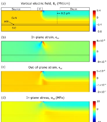
because there are no forces to prevent the top of the GaN buffer from moving. The bottom of the SiC substrate was constrained to zero displacement and the left and right boundaries of all layers were assigned a symmetry condition on the displacement so that they could only deform along the 𝑧-axis. In the 2D electro-mechanical model without the nucleation layer and substrate, the bottom of the GaN buffer was constrained to zero displacement. Contour plots of the resulting vertical electric field, strain, and stress distributions from the 3D electro-mechanical model in the 𝑥𝑧-plane at the center of the gate are shown in Figure 5.
FIG. 5. Results extracted from electro-mechanical model for GaN buffer in the pinched OFF state at 𝑉𝑑𝑠 = 20 V and 𝑉𝑔𝑠 = -6 V in the 𝑥𝑧-plane at the center of the gate (a) vertical electric field and (b) in plane strain, 𝜖𝑥𝑥 (c) out-of-plane strain, 𝜖𝑧𝑧, and (d) in-plane stress, 𝜎𝑥𝑥. The
dashed line in (a) indicates a line 0.5 µm to the left of the edge of the drain over which the depth-averages in the 𝑧-direction were computed.
The vertical electric field distribution in Figure 5(a) confirms that the vertical electric field is negative throughout the GaN buffer except for a narrow region directly under the gate contact.
30
In particular, the vertical 𝐸𝑧 component attains a peak value of -0.77 MV/cm at the edge of the
gate on the drain side and is fairly uniform in the gate-drain access region and under the drain contact in the 𝑥-direction. In the 𝑧-direction, the magnitude of the 𝐸𝑧 component decreases approximately linearly with 𝑧 from the top to the bottom of the GaN buffer due to formation of a space charge region associated with filled acceptor-type traps. At a location 0.5 µm to the left of the drain contact, the 𝐸𝑧 component attains a depth-averaged value of -0.165 MV/cm, which is equal to the drain bias divided by the thickness of the GaN buffer. Although the in-plane strain 𝜖𝑥𝑥 attains both negative and positive values of ~10-4 near the gate, it has a small depth-averaged positive value of 5.46 × 10⁻⁶ along the indicated cutline in the gate-drain access region in Figure
5(a). As shown in Figure 5(c), the out-of-plane strain 𝜖𝑧𝑧 closely resembles the 𝐸𝑧 distribution with negative values that vary linearly from the top to the bottom of the GaN buffer. The depth-averaged value in the gate-drain access region is -3.72 × 10⁻⁵, which is an order of magnitude larger than
that of the in-plane strain with the opposite sign. Finally, we found that the in-plane stress 𝜎𝑥𝑥 is
compressive in the gate-drain access region with an average value of -8.30 MPa.
The quantitative values of these strain and stress components are affected by the approximations of 2D plane strain in the 𝑥𝑧-plane (𝜖𝑦𝑦 = 0) and rigid clamping of the GaN buffer by the substrate. In Table I, we list values of the depth-averaged normal strain and stress components and the vertical electric field along the cutline 0.5 µm to the left of the drain contact from our electro-mechanical models with and without these assumptions.
31
TABLE I. Depth-averaged values of the strain, stress, and electric field components along the line 0.5 µm to the left of the drain contact calculated from the electro-mechanical model under
different approximations.
Quantity 2D plane strain without substrate
2D plane strain with
substrate 3D with substrate
𝜖𝑥𝑥 2.09 × 10⁻⁶ 6.46 × 10⁻⁶ 5.46 × 10⁻⁶ 𝜖𝑦𝑦 0 0 7.32 × 10⁻⁷ 𝜖𝑧𝑧 -3.61 × 10⁻⁵ -3.72 × 10⁻⁵ -3.72 × 10⁻⁵ 𝜖𝑥𝑦 0 0 -6.41 × 10⁻¹¹ 𝜎𝑥𝑥 (MPa) -9.53 -8.03 -8.30 𝜎𝑦𝑦 (MPa) -10.0 -9.53 -9.40 𝜎𝑧𝑧 (MPa) 0.065 0.046 0.019 𝐸𝑧 (MV/cm) -0.165 -0.165 -0.165
As shown in Table I, there is a tensile strain along the gate 𝜖𝑦𝑦 = 7.32 × 10⁻⁷ in the full 3D model
because the substrate cannot perfectly clamp the buffer from deforming along the 𝑦-direction. Since the strain components perpendicular to and along the gate are related through a strain compatibility relation [34] 𝜕2𝜖 𝑥𝑥 𝜕𝑦2 + 𝜕2𝜖 𝑦𝑦 𝜕𝑥2 = 𝜕2𝜖 𝑥𝑦 𝜕𝑥𝜕𝑦 (17)
the presence of non-zero 𝜖𝑦𝑦 in the full 3D model also slightly changes the value of 𝜖𝑥𝑥 compared
to the 2D models under the plane strain approximation. Rigid clamping of the bottom surface of the GaN buffer also results in lower values of the normal strain components and higher values of the normal stress components compared to the models with the nucleation layer and substrate included. In all cases, the out-of-plane strain 𝜖𝑧𝑧 is an order of magnitude larger than 𝜖𝑥𝑥 and two orders of magnitude larger than 𝜖𝑦𝑦. From Table I, one can see that there is a definite asymmetry
in the in-plane strain 𝜖𝑥𝑥 ≠ 𝜖𝑦𝑦 and in-plane stress 𝜎𝑥𝑥 ≠ 𝜎𝑦𝑦 in all cases but that |𝜎𝑥𝑥− 𝜎𝑦𝑦| ≪ |𝜎𝑥𝑥+ 𝜎𝑦𝑦|, both of which appear in Equation (9). Based upon these values obtained from
electro-32
mechanical modeling and past experimental observations that parallel and cross-polarized Raman scattering does not result in a splitting of the E2 high mode [13], we believe that the in-plane stress
is approximately symmetric (biaxial) and that Equations (11a) to (13) are valid.
Although the quantitative values of stress and strain obtained from the 3D electro-mechanical model is specific to the device described in Ref. [12], it does provide general insights into the electro-mechanical state of the buffer in GaN HEMTs in the pinched OFF state, which should guide interpretation of the experimental data from micro-Raman spectroscopy experiments. The mechanical constraint at the bottom of the GaN buffer associated with clamping by the substrate causes the depth-averaged in-plane strain to be one order of magnitude lower than the out-of-plane strain, i.e., |𝜖̅𝑥𝑥| ≪ |𝜖̅𝑧𝑧|. The free deformation of the top surface results in negligible
average out-of-plane stress (𝜎̅𝑧𝑧 = 0.019 MPa) through the depth of the GaN buffer compared to
the in-plane stress. This finding contradicts the hypothesis by Beechem et al. (2008) [8] that a significant stress along the 𝑐-axis is induced in the pinched OFF state, which the authors supposed by observing that the E2 high linewidth changes when the device is pinched OFF but remains
constant under an applied uniaxial stress in the 𝑐-plane. Upon further investigation, it was found that directly applying a mechanical stress along the 𝑐-axis slightly changed the E2 high linewidth
but with a much smaller magnitude than in the pinched OFF state [42], which supports our finding from the electro-mechanical model that |𝜎̅𝑧𝑧| ≪ |𝜎̅𝑥𝑥|. Considering the constitutive relation for the
out-of-plane stress and setting its value equal to zero while neglecting the in-plane strain (𝜖𝑥𝑥 ≈
𝜖𝑦𝑦 ≈ 0)
𝜎𝑧𝑧= 2𝐶13𝜖𝑥𝑥+ 𝐶33𝜖𝑧𝑧− 𝑒33𝐸𝑧 ≈ 0 (18)
33 𝜖𝑧𝑧≈
𝑒33
𝐶33𝐸𝑧 (19)
Since both constants 𝑒33 and 𝐶33 are positive, the out-of-plane strain 𝜖𝑧𝑧 should have the same sign as 𝐸𝑧, which is negative in the gate-drain access region in the pinched OFF state with a positive drain bias. Using similar relations for the in-plane stress components 𝜎𝑥𝑥 and 𝜎𝑦𝑦, one
can show that the stress state is expected to be compressive in the 𝑐-plane and approximately biaxial with 𝜎𝑥𝑥 ≈ 𝜎𝑦𝑦, which we confirmed with the electro-mechanical model (𝜎̅𝑦𝑦 = -9.40 MPa).
It is important to note that, based on the constitutive relations expressed averaged over a certain volume as in Equation (12) and confirmed by the electro-mechanical model, the average values of stress, strain, and electric field are related to each other by Equation (14). This fact is actually independent of the thickness of the GaN buffer and the mechanical boundary conditions needed to solve Equation (16). Although it has been previously suggested that the average stress and/or strain measured by micro-Raman spectroscopy could be related to the peak electric field obtained from electrical device modeling [14], this would violate Equation (14) and the electro-mechanical model presented in this work. If measured values of the stress and strain components from micro-Raman spectroscopy are much higher than those predicted by the average vertical electric field (approximately the drain bias divided by the buffer thickness), it is not physical to assume that they could be related to the much higher peak electric field. The only assumptions underpinning Equation (14) and this conclusion are that the GaN buffer behaves as a linear elastic, piezoelectric solid under the continuum approximation, which is widely assumed in both modeling and experimental studies in the literature [9],[35],[43].
34
IV. Material Properties
Because micro-Raman spectroscopy measures only the shift in phonon frequencies in the GaN buffer induced by a vertical electric field in the pinched OFF state, the material properties relating phonon frequency shifts to electric field must be accurately known. In particular, this involves the phonon deformation potentials, which relate the phonon frequency shifts to strain components according to Equations (7a) and (7b), and the elastic and piezoelectric constants, which relate stress, strain, and electric field components according to Equation (4). Since inaccuracies in the measured and/or calculated values of these properties have been suggested as a source of discrepancies between the observed and expected values of the stress and strain components in the pinched OFF state [12], we have taken the opportunity here to review and tabulate values of these properties from the literature. In anticipation of the analysis presented in Section V, we believe that the relatively small variation in these properties reported by different references particularly over the last five years on GaN samples with improving crystal quality are not a likely source of these discrepancies.
A. Elastic and Piezoelectric Constants
Both modeling and experimental characterization of the strain and stress induced in a GaN HEMT by the inverse piezoelectric effect require accurate values of the elastic stiffness 𝐶𝑖𝑗 or susceptibility 𝑠𝑖𝑗 constants and the piezoelectric strain 𝑑𝑖𝑗 or stress moduli 𝑒𝑖𝑗. Depending upon
whether the stress or strain components are known by measurement or simple approximations, alternate forms of the constitutive relations are useful. These constitutive relations, which are equivalent to Equation (4) for zero temperature change, can be written in two different forms by isolating the strain or stress components
35
𝜖𝑖= 𝑠𝑖𝑗𝜎𝑗+ 𝑑𝑘𝑖𝐸𝑘 (20a)
𝜎𝑖 = 𝐶𝑖𝑗𝜖𝑗− 𝑒𝑘𝑖𝐸𝑘 (20b)
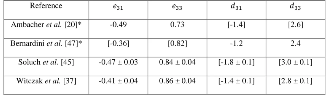
where the contracted notation for the strain, stress, elastic modulus, and piezoelectric modulus tensors has been used [25]. The elastic constants of GaN are typically reported in terms of the stiffness tensor 𝐶𝑖𝑗 from Brillouin scattering [44], surface acoustic wave [45], or bulk acoustic wave [37] experiments. Perhaps the most commonly cited reference for the elastic constants is that of Polian et al. (1996) [44] of a single crystal GaN needle with uncertainties of 10 to 20 GPa in the reported values. More recent measurements of the elastic constants on bulk GaN crystals grown by the ammonothermal method [37] report values in good agreement with Polian et al. (1996) but with uncertainties less than 1 GPa. Values of the elastic constants from three references are listed in Table II. A more exhaustive list of references including elastic constants determined from first principles calculations is available in Ref. [37]. As shown in Table II, the values reported by Witczak et al. (2015) [37] have the lowest measurement uncertainty and agree to within 10% with the values previously reported by Polian et al. (1996) [44], which were available at the time of publication of a number of early reports on inverse piezoelectric strain in GaN HEMTs [8], [12]-[14].
TABLE II. Elastic stiffness constants 𝐶𝑖𝑗 for wurtzite GaN (GPa).
Reference 𝐶11 𝐶12 𝐶13 𝐶33 𝐶44
Polian et al. [44] 390 ± 15 145 ± 20 106 ± 20 398 ± 20 105 ± 10 Soluch et al. [45] 345 ± 10 128 ± 5 129 ± 5 430 ± 10 96.5 ± 2 Witczak et al. [37] 366.9 ± 0.4 135.0 ± 0.6 97.5 ± 0.2 398.1 ± 0.6 99.1 ± 0.2
36
In contrast, values for the piezoelectric constants for wurtzite GaN vary significantly more among different references in the literature with higher measurement uncertainty than the elastic constants. Furthermore, some references report the piezoelectric strain moduli 𝑑𝑖𝑗 and others the piezoelectric stress moduli 𝑒𝑖𝑗 requiring use of a set of the elastic constants to convert between the
two forms [25]
𝑑𝑘𝑖 = 𝑒𝑘𝑗𝑠𝑗𝑖 (21a)
𝑒𝑘𝑖 = 𝑑𝑘𝑗𝐶𝑗𝑖 (21b)
Some differences in the reported values of the piezoelectric constants occur because of different measured or calculated values of the elastic stiffness or susceptibility constants appearing in Equations (21a) and (21b). A summary of the piezoelectric moduli values given in four references are shown in Table III. As in the case of the elastic constants, a more exhaustive review of values in the literature is given in Ref. [37]. All of the values of the piezoelectric stress and strain moduli from these four references differ by less than 20% from the most recent values published for bulk ammonothermal GaN crystals [37], except for the value of 𝑑31 from Ref. [45]. Some of the earliest values for the piezoelectric strain moduli 𝑑31 and 𝑑33 calculated from first principles by Bernardini
et al. (2002) [47] used in the analysis of the experimental data by Sarua et al. (2006) [12]
specifically are within 15% of the values measured recently by Witczak et al. (2015) [37], which themselves have low measurement uncertainties. Hence, we believe that uncertainty in the values of the elastic and piezoelectric constants available prior to 2006 are not a major factor in the uncertainty of the strain and stress values obtained by micro-Raman spectroscopy.
![FIG. 4. Electric potential distribution for the GaN HEMT structure reported in Ref. [12] for (a) the zero bias state](https://thumb-eu.123doks.com/thumbv2/123doknet/14475138.523057/26.918.278.642.103.581/electric-potential-distribution-structure-reported-.webp)