HAL Id: cea-01376969
https://hal-cea.archives-ouvertes.fr/cea-01376969
Submitted on 6 Oct 2016HAL is a multi-disciplinary open access archive for the deposit and dissemination of sci-entific research documents, whether they are pub-lished or not. The documents may come from teaching and research institutions in France or abroad, or from public or private research centers.
L’archive ouverte pluridisciplinaire HAL, est destinée au dépôt et à la diffusion de documents scientifiques de niveau recherche, publiés ou non, émanant des établissements d’enseignement et de recherche français ou étrangers, des laboratoires publics ou privés.
plasmonic self-organized crystal
Hugo Frederich, Clotilde Lethiec, Fangfang Wen, Julien Laverdant, Catherine
Schwob, Traian Popescu, Ludovic Douillard, Laurent Coolen, Agnès Maître
To cite this version:
Hugo Frederich, Clotilde Lethiec, Fangfang Wen, Julien Laverdant, Catherine Schwob, et al.. Plasmon excitation and induced emission with a plasmonic self-organized crystal. ICTON 2014, IEEE and IEEE PhotonicsSociety, Jul 2014, Grenz, Austria. pp.1-4, �10.1109/ICTON.2014.6876619�. �cea-01376969�
Plasmon Excitation and Induced Emission
with a Plasmonic Self-Organized Crystal
Hugo Frederich1,2, Clotilde Lethiec1,2, Fangfang Wen1,2, Julien Laverdant3, Catherine
Schwob1,2,Traian Popescu4, Ludovic Douillard4, Laurent Coolen1,2, and Agnès Maître1,2
1. Université Pierre et Marie Curie-Paris 6, UMR 7588, INSP, 4 place Jussieu, PARIS cedex 05, France 2. CNRS, UMR7588, INSP, Paris cedex 05, France
3. LPMCN, Université de Lyon, Université Lyon 1 and CNRS, UMR 5586, F-69622, Villeurbanne, France
4. Service de Physique et Chimie des Surfaces et Interfaces, CEA, IRAMIS, F-91191 Gif sur Yvette, France
ABSTRACT
In this paper, we describe the plasmonic and plasmon-photon coupling properties of nanostructured metallic films obtained by a self-assembly protocol. A gold layer is deposited on top of a self-assembled deposition of silica beads (artificial opal), which thus acts as a template. Atomic-force and scanning-electron microscopies demonstrates a periodic pattern on the metal surface with groove depth (here labelled h) ranging from 55 to 150 nm. By optical gonioreflectometry, the surface plasmon modes of this structure are probed: plasmon creation appears as an absorption dip in the reflection spectra. The plasmon dispersion relation is probed as a function of
h and shows, for the smaller values of h, a good agreement with an analytical model for vanishing h.
By depositing nanocrystals on the structure and measuring the fluorescence radiation pattern, we demonstrate a method to estimate the plasmon extraction (plasmon-to-photon coupling) efficiency. Finally, we use photo-emission electron microscopy to map the electric field of the plasmonic modes and characterize both propagative surface plasmon and localized (“hot spot”) plasmon modes.
Keywords: surface plasmons, self-organization, fluorescence, nanocrystals, electron microscopy. 1. INTRODUCTION
The coupling to a metallic surface is a promising way to enhance light emission and absorption [1], with applications in fields such as bio-imaging [2], light-emitting diodes (LED) [3], photovoltaics [4] or single-photon sources [5,6]. Surface plasmon polaritons (SPP), coupled propagating oscillations of the electric field and the charge movements at the surface of the metal, offer a wide range of possibilities to tailor the electric field. However, for planar metallic surfaces, the SPP modes cannot be converted to far-field propagating photons (and vice versa) because the phase matching condition cannot be fulfilled. The fabrication of a nanostructured
periodic grating on the metal surface is a possible way to allow plasmon-photon coupling.
We here analyse, by various characterization methods, the plasmonic properties and plasmon-photon coupling of such a metallic grating obtained by a self-organization protocol. Section 2 describes the sample fabrication and structural characterization. In Section 3, we probe the photon-to-plasmon conversion mechanism by gonioreflectometry. Almost 100-% light absorption is demonstrated due to the SPP mode. The SPP dispersion is studied as a function of the grating depth and compared to a theoretical model. In Section 4, we deposit colloidal nanocrystals on the metallic grating and use their near-field fluorescence to excite the SPP modes. By comparing the light emission diagram with theory and estimating the amount of SPP-mediated signal, we demonstrate a useful method to determine the plasmon-to-photon out-coupling efficiency (extraction efficiency). Finally, we use photo-emission electron microscopy to map the electric field of the photo-excited plasmonic modes. We evidence both SPP and localized plasmon (“hot spot”) modes.
2. SAMPLE STRUCTURE
Self-assembly offers many promising paths for nanostructuration. Opal samples (three-dimensionally ordered
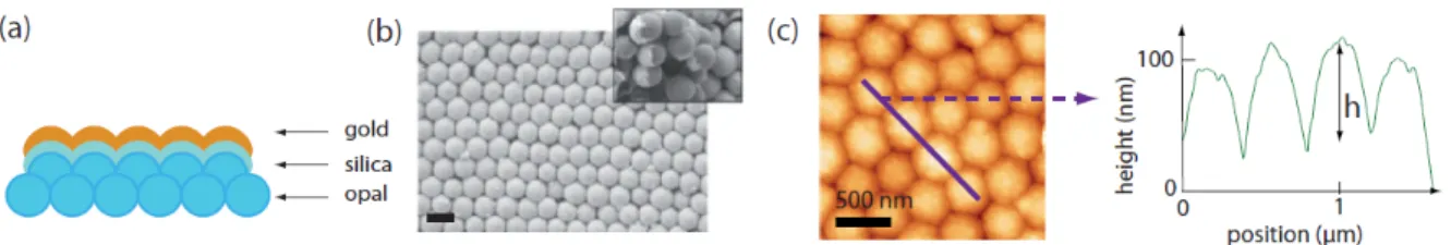
stacks of sub-micrometer spherical beads) have been the subject of many studies and their fabrication is now a mature technology [10]. We used a silica opal as a template in order to create a periodic pattern for a metallic film. The structure of the samples is indicated in Fig. 1a. A silica opal is covered by a gold layer (and sometimes a silica sub-layer is added in order to smooth the gold pattern). Scanning electron microscopy (SEM) (Fig. 1b) and atomic-force microscopy (AFM) (Fig. 1c) shows that the gold surface follows the 2D order of the opal template.
2
Figure 1: (a) Schematic of the fabricated structure; (b) Scanning electron microscopy image of a sample – scale bar: 500 nm (inset : damaged portion, showing the silica beads covered with gold); (c) Atomic-force microscopy image and profile of the sample.
We define the groove depth from the AFM profile as shown on Fig. 1c. By adjusting the gold and silica thicknesses, the obtained value of h can be tuned from 55 to 150 nm, as presented in table 1. The gold thickness is always much larger than the plasmon skin depth (typically 30 nm) so that the gold film can be considered infinite; the opal acts only as a template but does not contribute to the optical properties.
Table 1. Sample deposition parameters and corresponding obtained groove depth h (measured by AFM).
Beads diameter (nm) 390 390 390 390 390 390 480 480
Silica thickness (nm) - - - - 100 200 - -
Gold thickness (nm) 150 250 350 500 150 150 300 550
Groove depth h (nm) 150 130 100 90 75 55 130 110
We used opals obtained by a sedimentation protocol, as described in [9]. It is well established that such a protocol produces opals with 3D-ordered domains of typically tens of microns, with random in-plane orientations with respect to each other. Sections 3 and 4 will analyse the optical properties of the plasmonic gratings measured on sample portions of millimetre scales. The measured quantities will thus be averaged over all possible sample in-plane orientations. Further characterization of the sample order and disorder multiscale properties can be found in [7].
3. GONIOREFLECTOMETRY CHARACTERIZATION
We performed angle-resolved reflection measurements. The emission from a white halogen lamp was collimated as a 1-mm beam, passed through a polarizer and impinged on the sample with an angle θ controlled. The reflected light at the specular angle –θ was collected by an optical fiber and analysed by a spectrometer. The spectra were normalized but the spectrum of the lamp incident directly into the fiber. A typical result is shown on Fig. 2.
Figure 2. Specular reflection spectra in (a) p and (b) s polarizations, for a plasmonic sample of groove depth 90 nm (full lines) and for a flat gold film (dotted lines, divided by 2 for clarity), for various incidence angles θ ; (c )Schematic of the metallic grating first Brillouin zone and phase matching relation.
For a flat gold film (dotted lines), the reflection is almost complete at higher wavelengths and drops for wavelengths below 550 – 500 nm due to bulk gold absorption. The same feature appears on the plasmonic gratings reflection spectra, but dips also appear at certain wavelengths. We attribute these dips to absorption of the photons by creation of a plasmon mode. For s-polarized excitation, no SPP excitation is expected as SPPs are transverse-magnetic modes. A dip appears however below 600 nm in the measured spectra, which we attribute to the excitation of localized plasmonic modes as they show no dependence on the excitation angle. On the other hand, the dip in the p-polarized reflection spectra shows a strong spectral shift as a function of the incidence angle, which is a signature of SPP excitation. It is attributed to the excitation of a SPP mode, where the phase
matching condition between the incident photon in-plane wavevector k// and the SPP wavevector kSPP is fulfilled
due to the grating vector G4 (as defined on Fig. 2c). The dip reaches almost 0%, indicating that the
photon-to-plasmon coupling is extremely strong and that very efficient light absorption can be generated by this self-assembled grating.
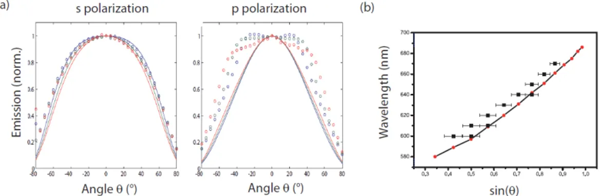
A similar feature appears for the p-polarized excitation spectra of all samples, as plotted on Fig. 3a. The dependence of the dip wavelength as a function of the angle (plotted in Fig. 3b as circles) is more pronounced for the lower groove depths. The line plots the theoretical correspondance for vanishing h, calculated by combining the phase matching condition (kSPP = k// + G4) with the theoretical dispersion relation ω(kSPP) of
a SPP mode on a planar gold surface, and averaging over all possible grating orientations φ to take into account the sample multi-domain disorder structure (see [7] for details). The measured curves indeed converge towards the theoretical one for decreasing h, validating the model.
Figure 3: (a) P-polarized specular reflection spectra for angles θ from 20 to 80°, for the 6 samples described in table 1 (groove depth h ranging from 150 to 55 nm); (b) Circles: wavelength of the measured reflection dip as a function of the incidence angle θ for the 6 samples. Line: theoretical line describing the case h = 0 (including the effect of averaging over all possible in-plane orientations as described in [7]).
4. FLUORESCENCE EMISSION DIAGRAM AND PLASMON EXTRACTION EFFICIENCY
In order to study the SPP out-coupling efficiency, we used the fluorescence of nano-emitters (CdSe/CdS nanocrystals, emission at 625 nm) to excite SPP modes (the near-field emission being coupled to the SPP, while the far-field is not). We sputtered on the sample an intermediate 80 nm silica layer to avoid quenching and then deposited the nanocrystals on silica. We performed angle and polarization-resolved emission spectra. The obtained emission diagram are plotted on Fig. 4a for several wavelengths. For the p-polarized emission, we
observed a wavelength-dependent peak of emission. We plot on Fig. 4b the relation between the wavelength and
the angle of this emission peak (black squares) and find that it matches the relation (red circles) obtained for this sample (after 80-nm silica coverage) for the dip in the reflection spectra. We thus attribute this peak in emission to the excitation of plasmon modes by nanocrystals and re-emission of plasmons to far field p-polarized radiation.
Figure 4: (a) Photoluminescence emission diagram (norm.) at 600 (blue), 630 (green) and 660 nm (red), in s and p polarizations, measured for nanocrystals on a plasmonic sample (circles) and calculated for nanocrystals on a flat sample (lines); (b) Correspondence between wavelength and angle of detection for the dip in specular reflection spectra (red circles) and for the peak in emission (black squares) at p polarization.
In order to quantize the efficiency of the extraction of SPP (probability that a SPP is scattered as a far-field photon), we compared the obtained spectra to the case of nanocrystals on a plane gold surface. We performed lifetime measurements in both cases to check that the corrugation has no influence on the emission rate and so
4 that the two configurations can be compared. We modelled the emission diagram of nanocrystals at 80 nm from a flat gold surface (lines on Fig. 4a) [11]. In s polarization, the theoretical flat gold curve is in good agreement with the measured grating curve, showing as expected to re-emission in s polarization. On the other hand, the p-polarized measured curves show a surplus of emission at the peak described above. This surplus can be quantified (see detail in [8]) and we found an extraction efficiency of 3% to 5% respectively at 600 and 660 nm, corresponding to an increase of 10% to 20% of the total emitted light. The experimental method developed here can be generalized to other systems and provides an interesting tool for designing light-extracting devices. 5. PHOTO-EMISSION ELECRON MICROSCOPY
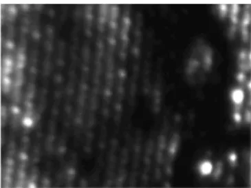
We used photo-emission electron microscopy (PEEM) in order to further characterize and distinguish the excited SPP or localized modes. PEEM provides a high-resolution (25-nm) mapping of the electric field of the photo-excited plasmonic modes. When excitation is performed in p polarization (Fig. 5), we find continuous electric field modulations which we attribute to the SPP modes. In both polarizations, localized “hot spots” appear, corresponding to localized plasmonic modes. The analysis of these images provides insight into the photon-plasmon coupling mechanism.
Figure 5. PEEM image under p-polarized excitation (the black shape on the right is an opal defect).
6. CONCLUSION
We discussed various characterization methods for a self-assembled plasmonic grating and analysed the coupling of far-field photons to SPP modes. By gonioreflectometry, almost complete photon absorption by SPP modes was demonstrated and characterized as a function of the groove depth. By using fluorescent nanocrystals as near-field SPP launchers, we demonstrated photon re-emission and quantified the extraction efficiency of this mechanism. Finally, PEEM can be used to provide further insight into SPP and localized plasmon modes and the role of defects.
REFERENCES
[1] W.L. Barnes, A. Dereux, and T.W. Ebbesen, Nature 424, 824 (2003); E. Fort and S. Grésillon, J. Phys. D 41, 013001 (2008).
[2] J.R. Lakowicz, Plasmonics 1, 5 (2006).
[3] J. Voucckovic, M. Loncar, and A. Scherer, IEEE J. Quantum Electron. 36, 1131 (2000).
[4] H.A. Atwater and A. Polman, Nature Mat. 9, 205 (2010); R. Esteban, M. Laroche and J.-J. Greffet, J. Appl.
Phys. 105, 033107 (2009).
[5] C. Vion, P. Spinicelli, L. Coolen, C. Schwob, J.-M. Frigerio, J.-P. Hermier, and A. Maître, Opt. Express 18, 7440 (2010).
[6] C. Belacel, B. Habert, F. Bigourdan, F. Marquier, J.-P. Hugonin, S. Michaelis de Vasconcellos, X. Lafosse, L. Coolen, C. Schwob, C. Javaux, B. Dubertret, J.-J. Greffet, P. Senellart, and A. Maître, Nano Lett. 13, 1516 (2013).
[7] H. Frederich, F. Wen, J. Laverdant, L. Coolen, C. Schwob, A. Maître, Optics Express 19, 24424 (2011). [8] H. Frederich, F. Wen, J. Laverdant, W. Daney de Marcillac, C. Schwob, L. Coolen, A. Maître, http://arxiv.
org/abs/1311.2269, accepted in Plamonics (2014).
[9] C. Vion, C. Barthou, P. Bénalloul, C. Schwob, L. Coolen, A. Gruzintev, G. Emelchenko, W. Masalov, J.-M.Frigerio, and A. Maître, J. Appl. Phys. 105, 113120 (2009).
[10] C. Lopez, Adv. Mater. 15, 1679–1704 (2003); F. Marlow, Muldarisnur, P. Sharifi, R. Brinkmann, and C. Mendive, Angew. Chem. Int. Ed. 48, 6212–6233 (2009).