HAL Id: cea-01615551
https://hal-cea.archives-ouvertes.fr/cea-01615551
Submitted on 12 Oct 2017
HAL is a multi-disciplinary open access
archive for the deposit and dissemination of
sci-entific research documents, whether they are
pub-lished or not. The documents may come from
teaching and research institutions in France or
abroad, or from public or private research centers.
L’archive ouverte pluridisciplinaire HAL, est
destinée au dépôt et à la diffusion de documents
scientifiques de niveau recherche, publiés ou non,
émanant des établissements d’enseignement et de
recherche français ou étrangers, des laboratoires
publics ou privés.
In situ cleaning of InGaAs surfaces prior to low contact
resistance metallization
Philippe Rodriguez, L. Toselli, E. Ghegin, N. Chevalier, N. Rochat, E.
Martinez, F. Nemouchi
To cite this version:
Philippe Rodriguez, L. Toselli, E. Ghegin, N. Chevalier, N. Rochat, et al.. In situ cleaning of InGaAs
surfaces prior to low contact resistance metallization. Microelectronic Engineering, Elsevier, 2016,
156, pp.91 - 96. �10.1016/j.mee.2015.11.013�. �cea-01615551�
In situ cleaning of InGaAs surfaces prior to low contact resistance metallization
Ph. Rodriguez
a,⁎
, L. Toselli
a, E. Ghegin
a,b, N. Chevalier
a, N. Rochat
a, E. Martinez
a, F. Nemouchi
aa
Univ. Grenoble Alpes, F-38000 Grenoble and CEA, LETI, MINATEC Campus, F-38054 Grenoble, France
b
STMicroelectronics, 850 rue Jean Monnet, BP 16, 38926 Crolles, France
a b s t r a c t
a r t i c l e i n f o
Article history: Received 28 June 2015
Received in revised form 30 October 2015 Accepted 25 November 2015
Available online 26 November 2015
In this work, we studied the pretreatment of InGaAs layers by employing Ar- and He-based direct plasmas and NH3, H2, NF3/NH3remote plasmas. All the remote plasmas involved in this study were inadequate to remove
the InGaAs native oxides. Moreover, for NF3/NH3exposed samples, we noticed the addition of undesirable In–F
and Ga–F bonds. Concerning Ar and He direct plasmas, investigations exhibited that both seem to be efficient for removing arsenic oxides whereas the elimination of indium oxides is more effective with Ar plasma. We also studied the addition of hydrogen into He direct plasma and we demonstrated that increasing the H2 content leads to decreasing the removal of arsenic oxides. The impact on indium oxides is also notable as we observed a reducing effect of hydrogen on indium and the emergence of In–In type bonds. Finally, whatever the plasma pretreatment, no degradation of surface morphology and roughness was observed by AFM. The RMS values obtained after surface treatments are similar with the ones acquired for reference samples.
© 2015 Elsevier B.V. All rights reserved.
Keywords: InGaAs Native oxides Surface pretreatment Direct plasma Remote plasma XPS FTIR 1. Introduction
The interest for contacting III-V materials has been growing since disruptive channel materials (including Ge and III-V materials) have been proposed for boosting the CMOS performance[1]. Studies are under progress in order to propose a contact science compatible with the Si CMOS technology. In this way, we observed a transition from non-self aligned technology to a self-aligned process[2,3]. Whatever the technology used (non-self aligned, self aligned, 3D…), cleaning technology is highly desirable for removing particles, organic materials, metallic impurities and native oxides. The classical salicide process (e.g. NiSi on Si or SiGe 30%) involves a two-step procedure where a wet HF treatment is coupled with an in situ plasma exposure[4]. Queue time related surface contamination and partial reoxidation caused by using only wet chemical cleaning is thus eliminated. For III-V contact technology, we assume that a similar strategy has to be devel-oped. If wet chemical cleanings are generally proposed for realising InGaAs n-MOSFET, in situ cleanings (plasma treatments realised in the same equipment as the metal deposition) have not been extensively studied. For deeply scaled transistors, parasitic resistances between the source and drain (S/D) regions and the metal contact have to be reduced as much as possible. Then, a very cleaned and native oxide free surface must be provided prior to metal deposition.
In this work, we propose a study using a Si CMOS technology compatible equipment in order to investigate the in situ cleaning of InGaAs layers. We introduce results obtained for various types of plasma processes (e.g. direct versus remote plasmas).
2. Experimental details
150 nm thick InGaAs layers grown by MOCVD on InP substrates (or Si wafers for ATR characterisations only) were used in this study.
NH3, H2, NF3/NH3remote plasma and argon and helium-based direct
plasma in situ pretreatments described in this work were carried out in a 300 mm Applied Materials Endura platform usually dedicated to silicide process and fully compatible with the Si CMOS technology.
Before direct plasma treatments, a degas step was performed at 200 for 30 s under argon atmosphere. Then, samples were treated into a direct plasma chamber without air exposure. Argon and helium direct plasmas were carried out using RF1 power ranging from 20 to 130 W and RF2 power ranging from 150 to 750 W and the etching duration was varied from 10 to 150 s. No substrate heating was performed during the plasma treatment. During the etching step, the chamber pressure ranged from 0.15 to 3.8 mTorr. These processes were calibrated on ther-mal silicon oxide to obtain process time versus silicon oxide equivalent thickness tables. 2.5 to 9 nm of silicon oxide are etched by the Ar direct plasma employed in this study (depending on the etching duration) whereas the He plasma does not affect significantly the silicon oxide layer (e.g. the difference of thickness measured after plasma treatment is under the spectroscopic ellipsometer sensitivity).
⁎ Corresponding author.
E-mail address:philippe.rodriguez@cea.fr(P. Rodriguez).
http://dx.doi.org/10.1016/j.mee.2015.11.013
0167-9317/© 2015 Elsevier B.V. All rights reserved.
Contents lists available atScienceDirect
Microelectronic Engineering
Concerning the remote plasma treatments, the samples were treated without previous degas step in a chamber maintained at 3 Torr during the etching step. The remote plasma power was set at 30 W and the process temperature wasfixed at 65. The etching step duration was varied from 60 to 300 s. After the etching step, a sublimation step was performed in the same chamber at 180 for 90 s.
Because 300 mm III-V wafers are not available, we used small pieces of InGaAs/InP on dedicated holders in order to process the samples in the 300 mm equipment.
The cleaning efficiency and impact on InGaAs surfaces have been studied on the CEA Minatec Nanocharacterisation Platform (PFNC) using surface analyses like X-ray photoelectron spectroscopy (XPS), atomic force microscopy (AFM) and Fourier transform infrared (FTIR) spectroscopy in attenuated total reflection (ATR) mode. XPS spectra were collected in a PHI VersaProbe II Scanning XPS Microprobe system using a monochromatic Al KαX-ray source. Ga 2p, Ga 3d, In 3d and As
3d spectra were collected with a constant pass energy of 23.5 eV leading to an overall energy resolution of 0.6 eV; curvefitting was done by CasaXPS 2.3.16 software. AFM measurements were performed in Tapping mode using a Bruker Dimension FastScan. For FTIR-ATR characterisations, the data were collected using a Ge prism pressed against the sample. A Bruker IFS 55 FTIR spectrometer probed the sam-ple via a P polarized infrared beam through the prism at an incident angle of 65, ensuring total reflexion on the Ge prism dioptre.
3. Results and discussion
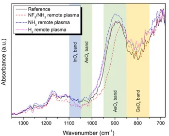
3.1. Comparison of remote plasmas versus Ar and He direct plasmas The effects on InGaAs layers of various remote plasma exposures have been investigated. Normalized Fourier transform infrared spectroscopy spectra in attenuated total reflection mode (FTIR-ATR) for InGaAs layers treated with NF3/NH3, NH3, H2remote plasmas and
without pretreatment are depicted onFig. 1.
Based on literature data[5,6], the absorption regions of InGaAs oxides are highlighted onFig. 1. The bands observed in the 1100– 1150 cm−1and 1150–1200 cm−1regions are not attributed to InGaAs
oxides but might be related to carbonaceous pollution from Ge prism or samples.
No significant effect of the different remote plasmas can be observed. Indeed, the absorption band of AsOXin the 850–950 cm−1region does
not seem to be impacted by the treatments. We can just notice that, for NF3/NH3exposed samples, the AsOXband seems to be narrowed or
slightly shifted towards low wavenumbers. Whatever the nature of the remote plasma, no significant reduction of the absorbance intensity of the AsOXband is observed. The same observation is drawn for InOX
and GaOXbands.
From the Ga 2p, In 3d and As 3dfitted XPS spectra (not shown here) of the remote plasma treated samples and for the reference sample, the corresponding relative spectral weight of the different components were extracted and are depicted onFig. 2. In 3d results are not shown here but the tendencies are similar to the gallium ones.
Fig. 1. Normalized FTIR-ATR spectra for InGaAs layers treated with NF3/NH3(dash red
line), NH3(dash dot blue line), H2(short dash magenta line) remote plasmas and without
pretreatment (solid black line).
Fig. 2. Relative spectral weight of the components determined for the NF3/NH3, NH3, H2
remote plasma treated samples and for a reference sample for Ga 2p (top) and As 3d (bottom) regions.
Fig. 3. Normalized FTIR-ATR spectra for InGaAs layers treated with Ar plasma (dash red line), He plasma (dash dot blue line) and without surface pretreatment (solid black line).
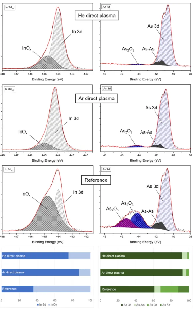
Fig. 4. XPS spectra peakfits of In 3d and As 3d regions for reference sample (bottom), Ar plasma treated sample (middle) and He plasma treated sample (top). The relative spectral weight of the components determined for the different samples is added.
XPS characterisations support the fact that remote plasma treatments involved in this study are not efficient at all for the removal of InGaAs oxides. The As5+component is still detected whatever the treatment
applied and the relative spectral weight of the bulk As 3d component of treated samples is similar to the reference sample one. Moreover, NF3/NH3remote plasma seems to significantly increase the As–As bond
(elemental arsenic) component to the detriment of As3+component
which might explain the slight shift observed for the corresponding FTIR-ATR spectrum. The analysis of the relative spectral weight of the components for the Ga 2p region confirms that the removal of InGaAs oxides is not achieved whatever the remote plasma treatment involved. Furthermore, for NF3/NH3exposed samples a third component appeared
in the XPS spectra of the Ga 2p and In 3d regions. These components are located at higher energies than oxide components and are attributed to undesirable Ga–F and In–F bonds.
Based on literature data[7,8,9], H2and NH3plasma treatments have
the ability to remove, or at least reduce the proportion of InGaAs native oxides. In this study no such effects were evidenced by exposing InGaAs layers to H2and NH3remote plasma. This phenomenon could be
ex-plained by the fact that the experimental conditions involved in this work were dictated by the remote plasma chamber used (experimental parameters could only be varied in a narrow range) and were different from the ones described in the abovementioned references, especially concerning the process temperature and pressure. Indeed, our experi-ments were carried out at lower temperature and at higher pressure which is not favourable for the desorption of by-products.
By comparison with remote plasma exposure and in order to pro-mote low temperature treatments, the impact of direct plasmas has been investigated.Fig. 3exhibits the normalized FTIR-ATR spectra for an InGaAs reference layer (i.e. native oxides without any treatments) and for InGaAs layers after Ar and He direct plasma processes.
We clearly observe differences between the spectrum obtained for an untreated sample and the spectra obtained for the plasma treated ones. Especially, the large absorption band of AsOxin the region of
850–950 cm-1
is drastically reduced after surface treatment. Both Ar and He direct plasma treatments seem to be efficient for eliminating the As oxides as indicated by the low absorbance intensity difference. While the impact of plasma treatment is less obvious on Ga and In oxides, it is also seen.
The corresponding In 3d and As 3d XPS spectra are shown onFig. 4. From thefitted XPS spectra, we extracted the corresponding relative spec-tral weight of the different components. After direct plasma treatments, thefitting of Ga 2p XPS spectra were difficult to obtain with accuracy, moreover for Ga 3d region, the In 4d components tend to parasite the Ga ones. Thus, tendencies for Ga will not be discussed here.
The XPS studies clearly evidence that both direct plasma treatments were efficient for reducing the percentage of InGaAs oxides. It is obvious for As oxides where the As2O5component is no more detected and the
As2O3is drastically reduced for treated samples. For In oxides, the
pro-portion of oxide components are significantly reduced compared to the reference sample. Nevertheless, for these elements, the oxide component after treatment is still important. Various hypothesis are currently under investigation for explaining these observations: the efficiency of the cleaning processes might be improved or the plasma treatments investigated in this study may preferentially lead to indium terminated surfaces which are partially reoxidised during the queue time (30 to 45 min) between the sample preparation and its surface characterisation.
Nevertheless, XPS analyses tend to confirm the FTIR-ATR observa-tions: both types of direct plasmas appear to be adequate for removing arsenic oxides. On the other hand, XPS investigations highlighted that Ar direct plasma is the most efficient for the removal of In oxides. Based on literature data[10], we believe that Ar plasma has an etching effect on InGaAs surface and that its native oxides are removed during this etching. Concerning the effect of He on InGaAs layers, we have exhibited a lack of literature data in order to elucidate the associated
mechanisms. However, due to a lower kinetic energy, we believe that He ions have only an etching effect on InGaAs native oxide surfaces and that InGaAs layer is not etched during the process.
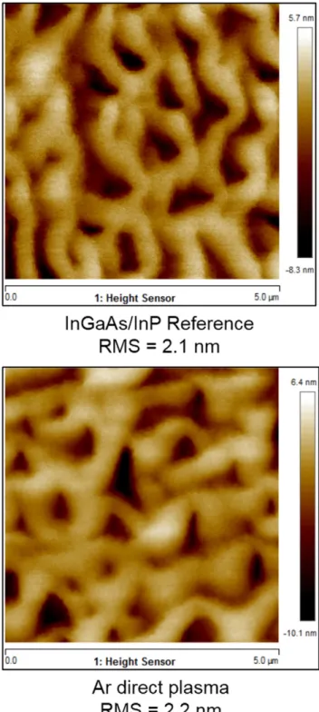
The impact of direct plasma treatments have been explored by AFM.
Fig. 5shows the AFM images obtained for the InGaAs/InP surface with-out any pretreatment (Reference) and the InGaAs surface after Ar treat-ment (the AFM image of sample after He plasma treattreat-ment is not shown here). AFM experiments have evidenced that, whatever the nature of the pretreatment, the surface morphology and roughness of InGaAs layers were not significantly impacted. RMS values are similar before (2.1 nm) and after plasma processing (2.2 nm for Ar and He direct plas-ma treated samples). Thus, for InGaAs surfaces with an initial roughness Fig. 5. AFM images for reference sample (top) and Ar direct plasma treated sample (bottom). The image space is 5 m × 5 m.
around 2 nm, no significant impact of plasma treatments has been highlighted.
3.2. Effect of hydrogen addition in He-based plasmas
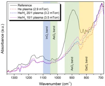
Fig. 6shows the normalized FTIR-ATR spectra for InGaAs layers
treated with He, He/H2 20/1, He/H2 10/1 plasmas and without
pretreatment.
From the results depicted onFig. 6, some tendencies can be drawn. First, the introduction of a slight percent of hydrogen in He-based plasma appears to modify the removal efficiency of the InGaAs oxides. The effect of hydrogen is visible not only for the large absorption band of AsOxin the 850–950 cm-1region but also for the narrower band in
the 1000–1050 cm-1region. Regarding the shape and the intensity of
the corresponding bands, AsOxremoval seems to be inversely
propor-tional to the H2plasma content. By only using FTIR-ATR analyses, the
effect of hydrogen addition in He-based plasma on indium and gallium oxide removal is less obvious.
From the In 3d and As 3dfitted XPS spectra (not shown here) of the He-based plasma treated samples with or without addition of hydrogen and for a reference sample, the corresponding relative spectral weight of the different components were extracted and are depicted onFig. 7. It should be noted that the addition of hydrogen into He plasma in-creases the pressure into the reactor during the sample pretreatment. As a result we also prepared additional samples treated with He direct plasma without addition of hydrogen but at higher pressure in order to evaluate the impact of this latter parameter.
The analysis of XPS results comforts the trends outlined by FTIR-ATR analyses. Addition of hydrogen clearly impacts the removal efficiency of InGaAs oxides. Indeed, increasing hydrogen content into He plasma leads to decrease the removal of arsenic oxides. As evidenced by comparing the samples treated with He plasma at 2.9 mTorr and at 3.8 mTorr, this trend might not only be attributed to hydrogen addition but could be related to the increase of pressure. Indeed, increasing the operating pressure is known to increase the ion scattering in the sheath and then to decrease the plasma efficieny[11]. On the other hand, if the increase of the pressure is clearly unfavourable for In oxides removal (compare the He plasma treated samples at 2.9 mTorr and at 3.8 mTorr), the addition of hydrogen seems to significantly impact the oxide removal. Indeed, compared to the reference sample, the relative spectral weight of the InOxcomponent appears to be reduced for the
samples treated with hydrogen. Moreover, hydrogen addition leads to the apparition of a third component in the XPS spectra of the In 3d
region. This component is located at approximately−0.8 eV from the bulk peak and is attributed to under coordinated indium at the surface or possibly indium dimers[12]. Thus, hydrogen addition might have a reducing effect on indium atoms. No such effect was observed on Ga XPS spectra.
4. Conclusion
We have investigated the impact of various plasma treatments on InGaAs layers. Argon- and helium-based direct plasmas are more ef fi-cient than remote plasmas for the removal of InGaAs native oxides. We have demonstrated that the nature of direct plasma influences the InGaAs oxide removal efficiency. Indeed, both types of plasma seem to be efficient for removing arsenic oxides whereas the elimination of In oxides is more effective with Ar plasma. Hydrogen addition in He plasma impacts the removal of InGaAs oxides and appears to have a reducing effect on indium atoms. Finally, whatever the nature of the pretreatment, the surface morphology and roughness of InGaAs layers were not significantly impacted.
Acknowledgements
The authors would like to thank Thierry Baron and his team (CNRS-LTM) for the realisation of InGaAs epitaxy and Nicolas Posseme for the fruitful discussions.
This project was supported by the public grant ANR-13-NANO-0001 MOSINAS, the Equipex FDSOI11 projects and the French national
programme“Programme d'Investissements d'Avenir” IRT Nanoelec
ANR-10-AIRT-05. Fig. 6. Normalized FTIR-ATR spectra for InGaAs layers treated with He (dash red line), He/H2
20/1 (dash dot blue line), He/H210/1 (short dash magenta line) plasmas and without
pretreatment (solid black line).
Fig. 7. Relative spectral weight of the components determined for the He-based plasma treated samples with or without addition of hydrogen and for a reference sample for In 3d (top) and As 3d (bottom) regions.
References
[1] S. Takagi, T. Iisawa, T. Tezuka, T. Numata, S. Nakaharai, N. Hirashita, Y. Moriyama, K. Usuda, E. Toyoda, S. Dissanayake, M. Shichijo, R. Nakane, S. Sugahara, M. Takenaka, N. Sugiyama, Carrier-transport-enhanced channel CMOS for improved power consumption and performance, IEEE Trans. Electron Devices 55 (1) (2008) 21–39,
http://dx.doi.org/10.1109/TED.2007.911034.
[2] Y.-C. Yeo, H.-C. Chin, X. Gong, H. Guo, X. Zhang, III-V MOSFETs: surface passivation, source/drain and channel strain engineering, self-aligned contact metallization, ECS Trans. 35 (3) (2011) 351–361,http://dx.doi.org/10.1149/1.3569928.
[3] S. Takagi, M. Takenaka, Prospective and critical issues of III-V/Ge CMOS on Si platform, ECS Trans. 35 (3) (2011) 279–298,http://dx.doi.org/10.1149/1.3569921. [4] S. Bonnetier, B. Imbert, M. Hopstaken, D. Galpin, R. Gwoziecki, D. Barge, S. Zoll, O. Anilturk, E. Sicurani, C. Caillat, A. Barr, R. Gonella, Y. Espinoux, P. Mur, N. Mayet, A. Gotti, M.-T. Basso, Silicide pre-clean effects on NiPtSi thermal stability for 65 nm technologies and beyond, Microelectron. Eng. 84 (11) (2007) 2528–2532,http:// dx.doi.org/10.1016/j.mee.2007.05.028.
[5] M. Rei Vilar, J. El Beghdadi, F. Debontridder, R. Artzi, R. Naaman, A.M. Ferraria, A.M. Botelho do Rego, Characterization of wet-etched GaAs (100) surfaces, Surf. Interface Anal. 37 (8) (2005) 673–682,http://dx.doi.org/10.1002/sia.2062.
[6] N. Liu, T.F. Kuech, Interfacial chemistry of InP/GaAs bonded pairs, J. Electron. Mater. 36 (3) (2007) 179–190,http://dx.doi.org/10.1007/s11664-006-0077-1.
[7] S.I.J. Ingrey, W.M. Lau, R.N.S. Sodhi, Characterization of surface oxides and oxide desorption on InGaAs, J. Vac. Sci. Technol. A 7 (3) (1989) 1554–1557,http://dx. doi.org/10.1116/1.576091.
[8] S. Habermehl, N. Dietz, Z. Lu, K.J. Bachmann, G. Lucovsky, Heteroepitaxial growth of Si on GaP and GaAs surfaces by remote, plasma enhanced chemical vapor deposi-tion, J. Vac. Sci. Technol. A 12 (4) (1994) 990–994,http://dx.doi.org/10.1116/1. 579077.
[9] H.-L. Lu, L. Sun, S.-J. Ding, M. Xu, D.W. Zhang, L.-K. Wang, Characterization of atomic-layer-deposited Al2O3/GaAs interface improved by NH3plasma pretreatment, Appl.
Phys. Lett. 89 (15) (2006) 152,910,http://dx.doi.org/10.1063/1.2363145. [10] J.E. Maslar, J.F. Dorsten, P.W. Bohn, S. Agarwala, I. Adesida, C. Caneau, R. Bhat,
Structural and electronic effects of argon sputtering and reactive ion etching on In0.53Ga0.47As and In0.52Al0.48As studied by inelastic light scattering, J. Vac. Sci. Technol. B 13 (3) (1995) 988–994,http://dx.doi.org/10.1116/1.588217. [11] E. Kawamura, V. Vahedi, M.A. Lieberman, C.K. Birdsall, Ion energy distributions in RF
sheaths; review, analysis and simulation, Plasma Sources Sci. Technol. 8 (3) (1999) R45,http://dx.doi.org/10.1088/0963-0252/8/3/202.
[12] B. Brennan, G. Hughes, Identification and thermal stability of the native oxides on InGaAs using synchrotron radiation based photoemission, J. Appl. Phys. 108 (5) (2010) 053,516,http://dx.doi.org/10.1063/1.3475499.