HAL Id: hal-02087930
https://hal.laas.fr/hal-02087930
Submitted on 2 Apr 2019
HAL is a multi-disciplinary open access
archive for the deposit and dissemination of
sci-entific research documents, whether they are
pub-lished or not. The documents may come from
teaching and research institutions in France or
abroad, or from public or private research centers.
L’archive ouverte pluridisciplinaire HAL, est
destinée au dépôt et à la diffusion de documents
scientifiques de niveau recherche, publiés ou non,
émanant des établissements d’enseignement et de
recherche français ou étrangers, des laboratoires
publics ou privés.
Understanding traps locations and impact on
AlGaN/GaN HEMT by LFN noise & transient
measurements, and T-CAD simulations
Jean-Guy Tartarin, Damien Saugnon, Oana Lazar, Guillaume Maillot,
Laurent Bary
To cite this version:
Jean-Guy Tartarin, Damien Saugnon, Oana Lazar, Guillaume Maillot, Laurent Bary. Understanding
traps locations and impact on AlGaN/GaN HEMT by LFN noise & transient measurements, and
T-CAD simulations. 2017 International Conference on Noise and Fluctuations (ICNF), Jun 2017,
Vilnius, Lithuania. pp.1-4, �10.1109/ICNF.2017.7985988�. �hal-02087930�
Understanding Traps Locations and Impact on
AlGaN/GaN HEMT by LFN noise & transient
measurements, and T-CAD simulations
J.G. Tartarin
1,2, D. Saugnon
1,2, O. Lazar
1,2, G. Maillot
1,2, L. Bary
1LAAS-CNRS1 and University of Toulouse, Université Paul Sabatier2
Toulouse, France tartarin@laas.fr
Abstract— Nitride technologies are widely used for high frequency and high power electronics, and raise a growing interest for robust low noise receivers. However, the stability of DC and RF performances are difficult to achieve, at a cost of technological trade-offs. Among the problems not totally mastered, traps and charges located in the active regions of the transistor induce a large variety of electrical behaviours; some traps are not harmful as they do not affect the transistor performances, some can impact the signal integrity or can raise reliability problems. The paper addresses a method based on low frequency noise (LFN) and random telegraph noise (RTN) measurements crossed with transient measurements and T-CAD simulations to locate the defects, and to evaluate their actual impact on the device integrity. This study is realized on virgin and stressed AlGaN/GaN High Electron Mobility Transistors (HEMT). Charges under the gated zone and at the AlGaN/GaN-passivation interface are identified by noise measurements and by T-CAD simulations.
Keywords—LFN and RTN; GaN HEMT; traps; T-CAD, reliability, HTOL stress.
I. INTRODUCTION
Nitride wide bandgap technologies position as a disruptive solution for the design of high power, high frequency modules [1]. AlGaN/GaN High Electron Mobility Transistors (HEMTs) are also convenient to design rugged Low Noise Amplifiers [2], taking advantage of low noise figures together with higher robustness versus RF harmful jamming signals. Using GaN based devices for electronic circuits improves the system density and reduces the overall weight of the system (reduction in the size of electronic circuits, power supply and heater or cooling system), with enhanced power capabilities. The increase in power density is bind to thermal induced effects (junction temperature) that still represents a first order issue for the reliability of these technologies. This paper proposes a cross-experimental non-invasive procedure using transient and low frequency harmonic measurements of noise parameters on drain or gate accesses, as well as T-CAD simulations to identify and locate traps in the active regions of the transistor [3]. These tools are used on a batch of virgin and stressed devices to track which effects can be considered as harmful during the application of a stress. In section two, the
technology under test is presented, with associated DC characteristics. Then, RTN and LFN noise characterizations are developed in the third section of the paper. In section four, T-CAD models and simulations are proposed to correlate with some previously discussed results. A conclusion gathers the main results of this paper.
II. TECHNOLOGIES UNDER TEST
Different technologies have been used to assess the proposed experimental procedures [4][5], resulting in improvement or qualification of the technology under test. Next, results on an intermediate step of the final technological declination (development phase) are reported. For this study, a High Temperature Operating Life stress test (HTOL) was applied on ten AlGaN/GaN HEMT devices featuring eight gate fingers, each featuring 125 µm width (the technology is 0.25 µm gate length), grown on SiC substrate. Measurements reveal a 45% drop on IDS (at VGS = 1 V and VDS = 8 V), a 130%
increase on RON, and one decade variation on IGS, after 105
hours of HTOL stress performed at 175°C ambient temperature (320°C junction temperature). The simultaneous degradation in the two dimension electron gas (2DEG) channel and gate command electrical characteristics make it difficult to interpret the results; obviously, a drop in the carrier density in the 2DEG can be related to transport degradation in the channel (presence of traps, drop of the mobility), or can be the consequence of the degradation in the control of this channel (i.e. a modification under the gate Schottky access). The presence of traps can be easily evidenced even during “DC-called” IDS-VDS output characteristics and IDS-VGS
transfer characteristics of the devices, for different setup of the signal analyzer used; Fig. 1 represents the output characteristics of a stressed device under test for high-medium-low configuration of Agilent 4156C signal analyzer. This procedure has been repeated several consecutive times, over several days, still demonstrating the same electrical behaviors between the 3 integration times (short, medium, long). It is obvious that DC characterization cannot be considered as a reference (stable) measurement, i.e. not sensitive to measurement setup conditions. The increasing or decreasing VDS sweeping conditions also can affect these
plots are attributed to the manifestation of traps featuring different time constants that change the output and transfer characteristics of the transistors under test (thermal effects are systematically accounted for in these plots). For that purpose, LFN harmonic measurements are performed between 1Hz and 100kHz.
Fig. 1. IDS-VDS DC output characteristics versus different VGS (+1V to -3.5V)
for a stressed device under short (80µs, −)medium (20ms, ---) long(320ms, −) integration times with Agilent 4156C Signal Analyzer.
It must be noticed that every stressed sample evidence the same trends on static characteristic (IDS drop and traps
manifestation according to experimental conditions as illustrated in Fig. 1), whereas the virgin samples feature a stable DC behavior. Pulsed I-V measurements have also been performed to evidence lag effects attributed to gate and to drain commands. Virgin devices are not strongly affected by lag (less than 2% variation on IDSS due to gate lag from -10V
to -5V VGS0 quiescent biasing conditions), whereas this gate
lag ranges from 7% to 15% for stressed devices. The drain lag for stressed devices is less than 5%.
III. LOW FREQUENCY NOISE MEASUREMENTS
LFN measurements can be used as an accurate sensor the improvement of the technological maturity for solid state devices assessment. But it is also a powerful tool for reliability investigations; as a noise source contributing to the LFN noise spectra is associated to a given defect occurring in a zone where the electrical signal flows (from gate to source for the gate current spectral density SIG or from drain to source for the
drain current spectral density SID); then its evolution can be
used as a precursor or as a marker of the degradation mechanism. For GaN devices, we are able to measure SIG and
SID for drain current below 200mA due to the biasing
networks limitations. If the correlation between SIG and SID is
close to zero then the noise contributions can be associated to specific defects at the gate (control) access and in the 2DEG channel (and contact resistances).
A. Gate access current LFN measurements SIG
SIG LNF spectra have been investigated for virgin and
stressed devices in diode mode (open drain and short circuited
drain) and in transistor mode (saturated). The spectra in diode mode feature extactly the same behavior according to the drain connection (open/short). A 1/fγ-like behavior is measured on
SIG for virgin and stressed devices in transistor mode,
featuring a linear dependance with IG (normalized as SIG/IG in
Fig. 2). The same trend for each transistor of the stressed or reference samples means an identical noise mechanism and electrical location for the noise sources contributor(s). Some distributed GR centers can be noticed on stressed devices between 100Hz-10kHz. Lorentzian can also be evidenced with higher contribution to the LFN spectra for virgin devices in diode configuration as illustrated in the inset of Fig. 2.
Fig. 2. Normalized gate current LFN spectral densities SIG/IG in transistor
mode for a virgin device and for a stressed device (VDS=20V, VGS=9V, 7V,
-5V, -3V, -2V, Vth=-3.5V). Inset is for SIG spectra of a virgin device biased in
diode mode only (VGS=-9V, -7V, -5V, -3V, -2V).
B. Drain access current LFN measurements SID
According to the maximum IDS that is allowed by our
experimental workbench (design of specific biasing networks for GaN devices), the transistors can only be investigated close to the pinch-off conditions (20% of IDSS max). However,
it is possible to discriminate some effects due to the space charge region (SCR) extension between gate and drain (constant IDS, VDG variable) or to the number of carriers in the
2DEG (constant VDG, VGS variable) as proposed in [6]. Figure
3 represents SID/ID for a constant drain current for a stressed
device (0.1A/mm, saturated biasing condition); however, in spite of some slight differences in GR locations within the spectra, virgin and stressed devices feature the same normalized SID/ID noise power densities. This means that the
40% drop on the static current IDS after HTOL stress is not
related to defects in the 2DEG, but more to mechanisms associated to the command under the gate or to the donor traps origin (surface states) of the 2DEG electron density [7][8]. The drain current noise spectra exhibit a monotonous decrease, but not featuring a 1/f like behavior. In Figure 3, only the magnitude changes with the increase of VDG, in
accordance with the extension of the SCR towards the drain access. An increase of SID(/ID) by 1.6 per drain voltage
corresponds to the activation of a larger noisy region under the gated zone towards the drain.
0 0,05 0,1 0,15 0,2 0,25 0,3 0 2 4 6 8 10 12 14 16 18 20 IDS (A /m m ) VDS(V) 0,4 0,5 0,6 0,3 0,2 0 0,1
Fig. 3. Normalized drain current LFN spectral densities SID/ID with constant
VGS bias (constant IDS=0.1A/mm) and variable VDS (VDG) for a stressed device.
C. Random Telegraph Noise on gate current
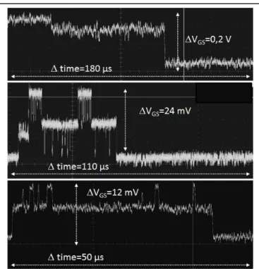
RTN noise measurements are also investigated to identify some potential trapping centers on the gate access (GR Lorentzian) as RTN noise contributors. A large variety of RTN is revealed on the gate access time domain measurements, with at least 6 different Lorentzian signatures featuring corner frequencies between 100Hz and 300kHz (i.e. out of the frequency domain measurement), and one RTN below 1Hz (Fig. 4 and Fig. 5). This frequency distribution of the Lorentzian can account for part of the 1/fγ gate current
spectral density (SIG in Fig. 2), whatever the biasing
conditions. The evolution of charges under the command can tune the real-time intrinsic bias of the gate (from 12mV to 200mV in Fig. 5), with the consequence of ΔIDS drain current
variations as evidenced in a shorter time window of 50s in Fig. 6 [9]. Over a long stress period, traps can accumulate both at the passivation-AlGaN interface layer and under the gate, each contributing to a drop in IDS. It is well known the major
role of surface donors as a major source contributing to the electron density in the 2DEG. VGS biasing plays an equivalent
contribution by shifting the energy levels in the channel and thus controlling the channel density till the pinch-off.
Fig. 4. example of Random Telegraph Noise on the gate access of a stressed device after 105 hours HTOL stress.
Fig. 5. different profiles of RTN time traces (stressed device). Measurements are performed trought a 100Ω resistor.
Fig. 6. Transient variation of IDS and IGS biasing currents versus time (0s-50s)
[9].
IV. T-CAD SIMULATIONS OF ALGAN/GANHEMT UNDER TEST
Non-invasive experimental techniques are extremely convenient to track the electrical signature of a defect contributing to DC or RF performances degradation. However, it can only allow speculative conclusions (even if with an elevated confidence level), as no intrinsic visual proof can be given of the defect. On another hand, destructive techniques such as EDX or TEM experiments give a direct proof of a defect, but cannot confirm the weight or even the proven action of the defect on electrical behavior; finally these destructive techniques can only be operated once per device (no intermediate measurement). Then, physical simulation using T-CAD software can strengthen the approach used in this paper once correctly calibrated for the process under test. Every physical parameter has been considered to design the model of the HEMT structure using Sentaurus solution.
0,5 0,52 0,54 0,56 0,58 0,6 0,62 0,64 0E+00 1E-07 2E-07 3E-07 4E-07 5E-07 6E-07 0 10 20 30 40 50 IDS (A) IGS (A) time (s) #NL IDS IGS
Fig. 7. T-CAD simulation of the conduction band versus fixed charges (FC) at SiN / GaN Cap interface for different FC densities
Meshing conditions under the gate and in the critical interface zones have been thoroughly studied to ensure convergence of the simulator and accurate results. Figure 7 represents the impact of the fixed charges density (FC) on the conduction band of the vertical structure. In this paper, single trap energy is considered to assess the previously identified impacts of (different) traps that impact DC, transient and noise spectra characteristics. Figure 8 corresponds to the different regions of donor concentration influencing the 2DEG sheet density as explained in [10].
Fig. 8. Simulation of the 2DEG electron density at zero bias as a function of the donor concentration, for different energies E0 of 0.2eV, 0.4eV and 0.6eV.
It has to be noticed that a change in the internal gate biasing voltage will lead to similar results on the fermi-level-not-pinned region (*) and fermi-level-fermi-level-not-pinned region (**), resulting in IDS drop by modification of gate bias induced energy
variation between trap and Fermi level (Et-EF). Moreover, from
IDS-VGS simulation versus nD, an IDS sensitivity to the donor
density is also found to be almost ΔIDS=70mA per ΔnD=1013
cm² of donor density fluctuation. For the HTOL stressed devices, under the assumption that only the donor concentration is responsible for the IDSS drop, a change of 45%
in IDSS implies an increase in donor state density of ΔnD=8.1013.
Of course, according to the low frequency and random telegraph noise measurements, several traps are involved in this Fermi-pining process, as proposed by Bakeroot in [8] (the 2DEG electron density is attributed to many discrete donor states.)
V. CONCLUSIONS
Experimental DC and RTN, LFN measurements have been developed on virgin and HTOL stressed devices to evidence the role of the traps in the degradation process of IDSS. DC,
pulsed or transient I-V measurements feature different behaviors. LFN and RTN studies have evidenced the presence of traps with corner frequencies spreading on a large time window (frequency range below 1Hz, up to 300kHz). These traps are more pronounced on stressed devices. Physical simulations of the structure with T-CAD tools have confirmed the crucial role of the trap states that impact the stability (real-time fluctuations) or the reliability (long term fluctuations) of AlGaN/GaN HEMTs under test. T-CAD feedbacks give consistent results with LFN analysis.
REFERENCES
[1] D. Floriot, V. Brunel, M. Camiade, C. Chang, H. BLanck, J. Grünenpütt, M. Hosch, H. Jung, “GH25-10 : New qualified power GaN HEMT process from technology to product overview”, 9th European Microwave
Integrated Circuit Conference, october 2014, Rome, Italy, 4p.
[2] S.D. Nsele, C. Robin, J.G. Tartarin, L. Escotte, S. Piotrowicz, O. Jardel, S. Delage, “Ka-band Low Noise Amplifiers based on InAlN/GaN technologies”, 23th International Conference on Noise and Fluctuations,
(ICNF 2015), June 2015, X’ian (China), 4p.
[3] G. Meneghesso et al., “Reliability issues of Gallium Nitride high electron mobility transistors”, Int. Journal of Microwave Wireless Technologies, vol. 2, no. 1, pp. 39-50, Feb. 2010.
[4] O. Lazar, J.G. Tartarin, B. Lambert, C. Moreau, J.L. Roux, J.L. Muraro, “New Approach for an Accurate Schottky Barrier Height's Extraction by I-V-T Measurements”, International Microwave Symposium IMS 2015, Phoenix, United States, 4p.
[5] J.G. Tartarin, “Diagnostic Tools For Accurate Reliability Investigations of GaN Devices”, 21th International Conference on Noise and
Fluctuations (ICNF 2011), Toronto (Canada), 12-16 Juin 2011, invited paper, 6p.
[6] J.G. Tartarin, G. Astre, S. Karboyan, T. Noutsa, B. Lambert, “Generation-recombination traps in AlGaN/GaN HEMT analyzed by time-domain and frequency-domain measurements: impact of HTRB stress on short term and long term memory effects”, International Wireless Symposium, 2013, China, 4p.
[7] J.B. Ibbetson, et al., “Polarization effects, surface states, and the source of electrons in AlGaN/GaN/GaN heterostructure field effect transistor”, Appl. Phys. Lett., vol. 77, no. 2, pp.250-252, jul. 2000.
[8] B. Bakeroot et al., “On the origin of the two-dimensional electron gas at AlGaN/GaN heterojunctions and its influence on recessed-gate metal-insulator-semiconductor high electron mobility transistors”, Journal of Applied Physics 116 (13), 134506, 2014.
[9] O. Lazar, J.G. Tartarin, B. Lambert, C. Moreau, J.L. Roux, “Correlation between transient evolutions of the gate and drain currents in AlGaN/GaN technologies”, Microelectronics Reliability 55 (2015), pp. 1714-1718.
[10] G. Longobardi, F. Udrea, S. Sque, G.A.M. Hurkx, J. Croon, E. Napoli, J. Sonsky, “Impact of Donor traps on the 2DEG and Electrical behavior of AlGaN/GaN MISFETs”, IEEE Electron Device Letters, vol. 35, no. 1, January 2014, pp.27-29.