HAL Id: hal-03080892
https://hal.archives-ouvertes.fr/hal-03080892
Submitted on 17 Dec 2020
HAL is a multi-disciplinary open access archive for the deposit and dissemination of sci-entific research documents, whether they are pub-lished or not. The documents may come from teaching and research institutions in France or abroad, or from public or private research centers.
L’archive ouverte pluridisciplinaire HAL, est destinée au dépôt et à la diffusion de documents scientifiques de niveau recherche, publiés ou non, émanant des établissements d’enseignement et de recherche français ou étrangers, des laboratoires publics ou privés.
A High Dynamic Range High Speed Pixel Operating at
100 Million Frames Per Second
Mathieu Hugoud, Wilfried Uhring, Jean-Baptiste Kammerer, Jean-Baptiste
Schell
To cite this version:
Mathieu Hugoud, Wilfried Uhring, Jean-Baptiste Kammerer, Jean-Baptiste Schell. A High Dy-namic Range High Speed Pixel Operating at 100 Million Frames Per Second. 18th IEEE Interna-tional New Circuits and Systems Conference (NEWCAS 2020), IEEE, Jun 2020, Montréal, Canada. �10.1109/NEWCAS49341.2020.9159819�. �hal-03080892�
A High Dynamic Range High Speed Pixel
Operating at 100 Million Frames Per Second
Mathieu Hugoud, Wilfried Uhring, Jean-Baptiste Kammerer, Jean-Bapstiste Schell ICube Laboratory
University of Strasbourg and CNRS Strasbourg, France [email protected]
Abstract— The burst imaging concept is a specific imaging
method than allows achieving a pixel rate of about 1 Tera pixel per second. This huge data rate can be reached by storing the video frames within the sensor, thus circumventing the bottleneck of the input/output of the sensor. Consequently, a frame rate of several Mega frames per second (Mfps) can be obtained and the use of a fast pixel front end is mandatory. In this paper, a pixel front able to operate at a frame rate of 100 Mfps is proposed. Based on a current mirroring integration approach, it offers a high dynamic range feature compatible with the record of the very fast moving object without blurring effect. The feature is carried out by mirroring in parallel the photocurrent into several integration capacitances. The pixel consumption is as low as 12 µW for one single gain branch at 10 Mfps and 118 µW at a frame rate of 100 Mpfs.
Keywords—High-speed imaging, CMOS, video sensor, current mirroring integration, burst imaging
I. INTRODUCTION
High-speed imaging is a key technology to study high-speed phenomena such as micromechanics, explosives, plasma formation mechanisms or laser ablation. The burst imaging concept introduced by Etoh allows to circumvolved the bottleneck of the data input/output of the sensor by storing the series of images within the sensor [1]. This way, a pixel rate of about 1 terapixel per second can be achieved while the conventional approach that extracts continuously the frames from the sensor is limited to a few tens of Gigapixel per second [2]. Thus, a frame rate of several Megaframe per second (Mfps) can be achieved with a spatial resolution of about 1 megapixel [3] and a frame rate of several Gigaframe per second has been demonstrated with a streak camera approach with a reduced spatial resolution [4]. At such a frame rate, the exposure time is very short, thus the pixel analogue front end has to operate at a high speed while providing a high gain. In addition, the concept of storing the pixel within the sensor is relevant in the framework of a 3D stacked integrated circuit approach. Indeed, storing the images in an additional tier allows to save space on the first one that could be utterly dedicated to the sensitive part of the pixel in order to increase the fill factor. Additionally, the supplementary tier allows storing more frame in order to increase the movie length [3] . Moreover, pushing the 3D stacked up to 3 or more tiers makes it possible to implement more on chip functionality such as analogue to digital conversion [5][6].
Several high-speed pixel front-end architectures have been reported such as CCD[7], pinned photodiodes [3], buffered and non buffered direct injection [8], Classic 4T pixel [5] or capacitive feedback transimpedance amplifiers [6], but none of these architectures offers a High Dynamic Range (HDR) feature. The HDR feature consists to capture an image with very different intensity levels without saturating. i.e., the brighter part of the image are not saturated to the maximum level and the darkest part of the image are not saturated to the
minimal value. The classical operation of an HDR acquisition rely on the acquisition of several frames with varied integration time. Nevertheless, this mode of operation is incompatible with the acquisition of a very fast event as a blurring effect occurs while recording fast-moving objects. This paper presents a new architecture of high-speed pixel front end featuring a single shot HDR operating at up to 100 Mfps based on a Current Mirroring Integration (CMI) approach. Several gains are obtained in parallel with the integration of the photocurrent into some capacitances of different values with a single frame acquisition.
The architecture and operation of the pixel are presented in section 2. The pixel performances are assessed thanks to simulation results shown in section 3. The design constraints related to mismatch are then presented in section 4.
II. SYSTEM DESCRIPTION
The proposed architecture is based on a CMI approach that consists in copying the photocurrent Iph flowing through the
photodiode into an independent capacitance Cint as shown in
Fig. 1. The benefits of this technique is twofold, 1) it allows to keep a constant bias on the photocathode, improving the photodiode transient response and 2) it allows separating the conversion gain from the photodiode capacitance, increasing the pixel sensitivity. Indeed, in the case of a high speed burst image sensor the pixel pitch is generally a few tens of micrometres, thus the photodiode area is relatively high. As a consequence, the capacitance of the junction Cdiode is
generally high and integrating the photo-charge directly within the photodiode leads to a low conversion gain whereas mirroring the photocurrent in a smaller capacitance Cint with
Cint << Cdiode offers a high conversion gain.
Nevertheless, a high conversion gain can result in saturation of the pixel response in the case of a too strong light exposure. A HDR image sensor provides an image where the pixels with a higher illumination aren’t saturated but still have an intensity related to its illumination. To provides this feature, we added some additional mirrored current integrating the photo-charge into different capacitances Cintn.
Fig. 1. Principle of the Current Mirroring integration pixel with HDR feature
The schematic of the pixel is detailed in Fig. 2. The current mirror that copy the photo-current Iph from the photodiode to
the integration capacitance Cint is formed by M9-M10. In order
to operate at a frame rate of 10 or 100 Mfps, the bandwidth of this current mirror has to be higher than 10 or 100 MHz. But this bandwidth can’t be achieved without a DC biasing current flowing through the current mirror. Thus, an external source feeds the current Ibias into the current mirror M1-M2 to provide
an additional current Ibias into the M9-M10 current mirror.
Note that this biasing current can be externally adjusted to match the required bandwidth in regards to the acquisition frame rate.
The resulting current Iph+Ibias is mirrored into the Cint
capacitance and a supplementary current mirror formed by M1-M6 withdraw the biasing current Ibias from the Cint
capacitance. Providing that the current mirrors are perfectly matched, only the photocurrent Iph charges the integration
capacitor Cint resulting in a voltage increase ∆Vout at the output
node given by:
(
I
biasM10−
I
biasM6+
I
ph)
⋅ =
dt
I
ph⋅ =
dt C
int⋅ ∆
V
out∫
∫
(1) Where 10 M biasI
and 6 M biasI
are respectively the current mirrored by the transistor M10 and M6.In order to improve the current mirror matching, the cascode transistors M3, M4 and M5 ensure than the current mirrors formed by current M1-M2 and M6 are always identically biased. In the same way, the cascode transistors M7 and M8 ensure that the current mirror formed by M9 and M10 are biased similarly. This in particularly useful as the Out voltage is varying as the photocurrent is integrated while the photodiode voltage is almost constant.
Finally, the transistor M11 is used to reset the output voltage to an intermediate voltage ensuring the good operation of the current sources. The maximum output voltage is:
𝑂𝑂𝑂𝑂𝑂𝑂𝑚𝑚𝑚𝑚𝑚𝑚= 𝑉𝑉𝐷𝐷𝐷𝐷− 𝑉𝑉𝐷𝐷𝐷𝐷(𝑠𝑠𝑚𝑚𝑠𝑠)𝑀𝑀8− 𝑉𝑉𝐷𝐷𝐷𝐷(𝑠𝑠𝑚𝑚𝑠𝑠)𝑀𝑀10 (2)
The minimum output voltage depends on the potential at the reset transistor node. Therefore, the theoretical voltage output range is given by:
∆𝑉𝑉𝑂𝑂𝑂𝑂𝑂𝑂 = 𝑉𝑉𝐷𝐷𝐷𝐷− 𝑉𝑉𝐷𝐷𝐷𝐷(𝑠𝑠𝑚𝑚𝑠𝑠)𝑀𝑀8− 𝑉𝑉𝐷𝐷𝐷𝐷(𝑠𝑠𝑚𝑚𝑠𝑠)𝑀𝑀10+ 𝑉𝑉𝑟𝑟𝑟𝑟𝑠𝑠𝑟𝑟𝑠𝑠
Finally, the different conversion gains are obtained by adding n times the last branch of the circuit with some different integration capacitance Cintn. Obviously, the gain can also be
adjusted by varying the ratio of the current mirror. An additional system, not shown in Fig. 2, is mandatory to select the good output in regards of its value. The selection algorithm consists to select the higher gain output which is not saturated for the correspondent image value to be stored. An information coded in a analog or a digital format is also added to know at which gain the image value has been stored. As a consequence, an image is composed of a gain value and an analog value. The next section presents the simulation results of the front-end circuit.
I. CIRCUIT PERFORMANCE
The proposed circuit has been designed in a 180 nm CMOS image sensor technology and simulated using SpectreTM. The
photocurrent is modeled using a homemade Verilog-A photodiode compact model, allowing a realistic representation
Fig. 2. Schematic diagram of the pixel circuit
of the current pulse which is integrated over Cint. The
photodiode model describes the behavior of a NWell over Psub
photodiode with the assessment of the doping profiles for the used technology. For the higher conversion gain branch, the integration capacitor Cint is set to 10 fF which is close to the
parasitic capacitors and buffer input capacitor values. Two low gain additional branches have been added with an integration capacitance of respectively 50 and 100 fF. Fig. 3 and 4 show the simulation results at a frame rate of 10 Mfps and 100 Mfps. In order to match the required bandwidth, the Ibias current has
been set to respectively 1.2 µA and 12 µA for the frame rate of 10 and 100 Mfps. A new frame starts with the release of the reset which initialized the output voltage to 1.1 V. The VDD
power supply is set to 3.3 V to achieve a high output voltage range close to 1.8 V. Two pulses of light are emulated on frame 2 and 4 thank to the photodiode model. The pulses start at the very beginning of the specified frames and last for half the period of a frame exposure.
Fig. 3. Circuit simulation at 10Mfps, Ibias = 1.2µA, generated photocurrent
(dashed line), output voltage with a integration capacitance of 10 fF (red), 50 fF (green) and 100 fF (Blue)
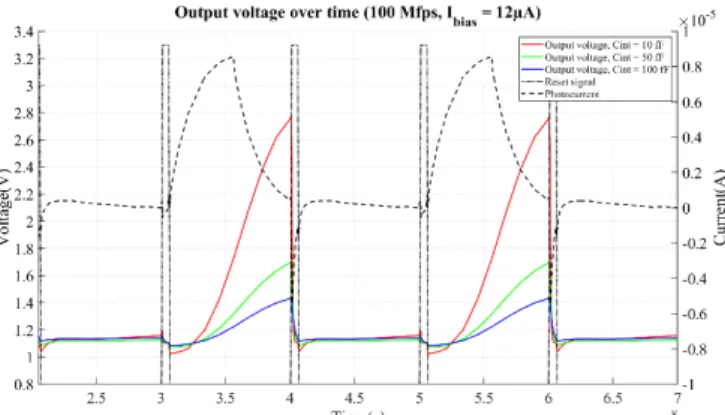
Fig. 4. Circuit simulation at 100Mfps, Ibias = 12µA, generated photocurrent
(dashed line), output voltage with a integration capacitance of 10 fF (red), 50 fF (green) and 100 fF (Blue)
At a frame rate of 10 Mfps the generated photocurrent by the pulse of light is set to 800 nA (black dashed line in Fig. 3). The rounded shape of the photocurrent is due to the internal capacitance of the photodiode. This pulse of light is sufficient to bring the higher gain branch close to the saturation (red line in Fig. 3) with a voltage swing of about 1.7 V. With a bias current Ibias of only 1.2 µA, the bandwidth of the pixel is adequate to integrate the light pulse with a total absence of lag on the next frame. Indeed, the output is rising as long as the photocurrent is generated and stop rising as the photocurrent return to zero. The reset width set to 6 ns is long enough to completely reset the output node. The lower gain branch responses are also depicted in Fig. 3 (green line for 50 fF and blue line for 100 fF). The simulated conversion gains at respectively 10 fF, 50 fF and 100 fF are equal to 6.8µV/e-, 2.6µV/e- and 1.4µV/e- corresponding to an equivalent integration capacitance of 23 fF, 62 fF and 114 fF. The parasitic capacitances of the output node are thus assessed to be 13 fF. The power consumption at this frame rate is of only 12 µW for one single gain branch and supplementary consumption of 4 µW is added for each additional gain branch. The simulation results at a frame rate of 100 Mfps are depicted in Fig. 4. At this frame rate, the generated photocurrent by the pulse of light is set to 8 µA (black dashed line) to reach the saturation of the high-gain branch (red line) with a voltage swing of about 1.7 V. At a period of only 10 ns, the response of the photodiode is close to its limit as the photocurrent only have the time reaches 8 µA before returning to zero. Nevertheless, the total charge remains proportional to the light pulse energy and the response of the pixel at a bias current Ibias
increased up to 12 µA is close to the 10 Mfps configuration as the final voltages reach almost the previous ones. This indicates that the bandwidth of the pixel is adequate and it is confirmed by the absence of lag on the next frame. In this simulation, the reset width is as short as 600 ps allowing an almost full aperture of the exposure time. The lower gain branch responses (green line for 50 fF and blue line for 100 fF) are also reaching the same final voltage. The simulated conversion gains at respectively 10 fF, 50 fF and 100 fF are equal to 6.6 µV/e
-, 2.4 µV/e- and 1.2 µV/e-. This result
confirms that the pixel is able to operate at 100 Mfps The power consumption at this frame rate is 118 µW for one single gain branch with a supplementary consumption of 49 µW per additional gain branch.
II. DESIGN CONSTRAINTS
The previous results showed that the current biasing technique of the current mirrors ensure a sufficient bandwidth event at 100 Mfps. Nevertheless, the current mirrors are particularly susceptible to device mismatch that can lead to a non-zero output current for a null photocurrent. Indeed, in this circuit, due to the effect of mismatches, the
10 M bias
I
and 6 M biasI
current could not be exactly compensated and thus, the integration capacitor Cint could be charged or discharged even
with a null photocurrent Iph (see equation (2)).
In order to evaluate the effect of the mismatch on the pixel operation, a Monte Carlo analysis has been performed. The literature shows that a correlation coefficient over 0.9 is easily achievable with a common-centroid layout structure [13][14][13]. Therefore, a correlation coefficient of 0.9 is introduced between each transistor of the pixel.
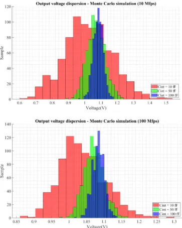
Fig. 5 shows the Monte-Carlo simulation of the output voltage for a null photocurrent at a frame rate of 10 Mfps. The dispersion of the output due to the mismatches is higher for the
Fig. 5. Monte-Carlo simulations of the output node at 10 Mfps (up) and 100 Mfps, without photonic current,i.e. dark image. The results represent the fixed patern noise (FPN).
high gain compared to the lower gain. Indeed, the compensation mismatch of the current at the output node is amplified by the conversion gain of this node. The peak to peak value of the dispersion are respectively 1 V, 340 mV and 190 mV for the 10 fF, 50 fF and 100 fF gain branch.
These values are not negligible and they clearly highlight a drawback of the approach. However, this flaw can be compensated with a correlated double sampling feature and it can be seen as a simple Fixed Pattern Noise (FPN). Indeed, the subtraction of an image acquired in the dark can efficiently suppress this static dispersion. Moreover, the high-gain branches of the worst pixels still offer a large dynamic of 1.2 V and even if this branch of the pixel is saturated, the HDR feature ensure that the signal is still measurable on a lower gain branch. The Monte Carlo simulation of the output dispersion at a frame rate of 100 Mfps is also shown on Fig. 5. The peak to peak value of the dispersion is better to the previous one with respectively 450 mV, 200 mV and 120 mV for the 10 fF, 50 fF and 100 fF gain branch. This indicates that the pixels can still operate at the frame rate of 100 Mfps.
The pixel response non uniformity (PRNU), i.e. the dispersion of the pixel response when a spatially uniform light is applied on the sensor has also be assessed thanks to a Monte Carlo simulation. The response of a pixel to a given constant photocurrent is evaluated by subtracting the voltage of a pixel when the light is applied and the voltage of the same pixel when no light is applied. The relative dispersion of the pixel response, i.e. the ratio between the rms dispersion of the output and the mean value of the pixel has been simulated at a gain of 10, 50 and 100fF and a frame rate of 10 and 100 Mfps. The results obtained at 100 Mfps are depicted in Fig. 6. The assessed PRNU is as low as 1% and can be characterized and compensated by post processing. This results also shows that the relatively high FPN can be efficiently measured and
Fig. 6 Monte-Carlo simulations of the output node at 10 Mfps (up) and 100 Mfps, with photonic current,i.e. bright image. The results represent the pixel response non uniformity (PRNU).
withdrawn and thus is not a critical issue of the proposed architecture.
A transient noise analysis has also been performed in order to assess the signal-to-noise ratio (SNR) of the pixel. The output noise is in the range of a few mV (see table I and table II) and is obviously reduced on the lower gain branches due to the presence of a higher integration capacitance keeping the input referred SNR almost constant.
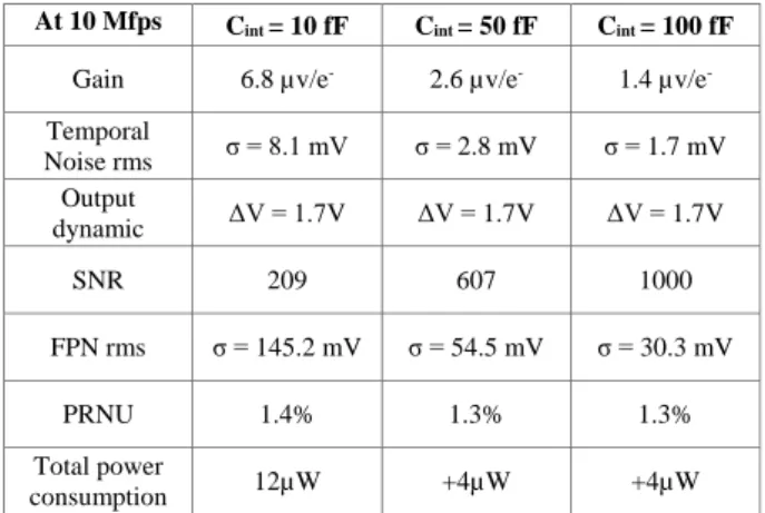
TABLE I. SIMULATION RESULTS AT A FRAME RATE OF 10MFPS
At 10 Mfps Cint = 10 fF Cint = 50 fF Cint = 100 fF
Gain 6.8 µv/e- 2.6 µv/e- 1.4 µv/e
-Temporal Noise rms σ = 8.1 mV σ = 2.8 mV σ = 1.7 mV Output dynamic ΔV = 1.7V ΔV = 1.7V ΔV = 1.7V SNR 209 607 1000 FPN rms σ = 145.2 mV σ = 54.5 mV σ = 30.3 mV PRNU 1.4% 1.3% 1.3% Total power consumption 12µW +4µW +4µW
TABLE II. SIMULATION RESULTS AT A FRAME RATE OF 100MFPS
At 100 Mfps Cint = 10 fF Cint = 50 fF Cint = 100 fF Gain 6.6 µv/e- 2.4 µv/e- 1.2 µv/e
-Temporal Noise rms σ = 5.4 mV σ = 5.1 mV σ = 2.7 mV Output dynamic ΔV = 1.7V ΔV = 1.7V ΔV = 1.7V SNR 314 333 629 FPN rms σ = 63.1 mV σ = 28.1 mV σ = 17 mV PRNU 0.9% 1% 1.6% Total power consumption 118µW +40µW +40µW CONCLUSION
A high-speed pixel architecture well suited for high speed burst image sensor is proposed. It offers a multi-HDR feature carried out with a single frame exposure which is a mandatory functionality in the framework of ultrafast imaging. The pixel counts 11 transistors for a complete gain branch plus 5
transistors for each additional gain branches. The simulation results shows that the pixel is able to operate at a frame rate from 10 Mfps up to 100 Mfps. The biasing current of the pixel as to be adjusted in regards of the required frame rate. The pixel consumption is as low as 12 µW for one single gain branch at 10 Mfps and 118 µW at a frame rate of 100 Mpfs. To the best of our knowledge, it is the very first pixel dedicated to burst imaging sensors that provides an HDR feature.
ACKNOWLEDGMENT
This project has received funding from the European Union's Horizon 2020 research and innovation programme under grant agreement No 777222 through the ATTRACT Digital Burst Image Sensor (DIBIS) Project.
III. REFERENCES
[1] T. G. Etoh, Kohsei Takehara, K. Takehara, "Ultrahigh-speed multiframing camera with an automatic trigger", Proc. SPIE 1757, Ultrahigh- and High-Speed Photography, Videography, and Photonics, 1993; doi: 10.1117/12.139154
[2] https://www.phantomhighspeed.com/products/cameras/ultrahighspeed /v2640, phantom Website
[3] M. Suzuki, Y. Sugama, R. Kuroda and S. Sugawa, “Over 100 Million Frames per Second 368 Frames Global Shutter Burst CMOS Image Sensor with Pixel-wise Trench Capacitor Memory Array, “ Sensors 2020, 20(4), 1086; https://doi.org/10.3390/s20041086
[4] M. Zlatanski , W. Uhring, J-P. Le Normand, “Sub-500 ps Temporal Resolution Streak-mode Optical Sensor,” IEEE Sensors Journal, pp. 6570-6583, Vol. 15 (11), 2015, doi:10.1109/JSEN.2015.2462021 [5] L. Millet , M. Vigier , G. Sicard , N. Magotat , F. Guellec , W. Uhring,
“A 5 Million Frames Per Second 3D Stacked Image Sensor With In-Pixel Digital Storage,” ESSCIRC, 44th European Solid-State Circuits Conference, pp. 62-65, 2018, doi:10.1109/ESSCIRC.2018.8494287 [6] W. Uhring, L. Millet , B. Misischi, F. Rarbi , F. Guellec , D. Dzahini ,
O. Maciu, J-B. Kammerer, G. Sicard, “A Scalable Architecture for Multi Millions Frames per Second CMOS Sensor With Digital Storage,” IEEE NEWCAS, pp. 252-255, 2018, doi:10.1109/NEWCAS.2018.8585644
[7] J. Crooks,B. Marsh, R. Turchetta, K. Taylor, W. Chan, A. Lahav, A. Fenigstein, “Kirana: a solid-state megapixel uCMOS image sensor for ultrahigh speed imaging.” Proc. Of SPIE Vol. 8659, p. 865903, 2013, doi.org/10.1117/12.2011762.
[8] R. Bonnard, J. Segura , F. Guellec , W. Uhring, “signal conditioning circuits for 3D -integrated burst image sensor with on-chip A/D conversion,” Image Sensors and Imaging Systems 2015, Vol. 9403, n° 940304, 2015, doi:10.1117/12.2082534
[9] M. Ahmed and A. Bermak, "A CMOS Current Mirroring Integration Based Visible Light Receiver for Intelligent Transport Systems," 2019 IEEE 62nd International Midwest Symposium on Circuits and Systems (MWSCAS), Dallas, TX, USA, 2019, pp. 556-569.
[10] W. Zhang, Y. Pan and L. Meng, "A X-Ray CMOS Image Sensor Based on Current Mirroring Integration Readout Circuit," 2012 International Conference on Computer Science and Electronics Engineering, Hangzhou, 2012, pp. 592-595.
[11] M. Tepegoz and T. Akin, "A readout circuit for QWIP infrared detector arrays using current mirroring integration," ESSCIRC 2004 - 29th European Solid-State Circuits Conference (IEEE Cat. No.03EX705), Estoril, Portugal, 2003, pp. 133-136.
[12] C. H. Hwang, C. B. Kim, Y. S. Lee and H. C. Lee, "Pixelwise readout circuit with current mirroring injection for microbolometer FPAs," in Electronics Letters, vol. 44, no. 12, pp. 732-733, 5 June 2008. [13] Mao-Feng Lan and R. Geiger, "Matching performance of current
mirrors with arbitrary parameter gradients through the active devices," 1998 IEEE International Symposium on Circuits and Systems (ISCAS), Monterey, CA, 1998, pp. 555-558 vol.1.
C. F. T. Soares and A. Petraglia, "Automatic Placement to Improve Capacitance Matching Using a Generalized Common-Centroid Layout and Spatial Correlation Optimization," in IEEE Transactions on Computer-Aided Design of Integrated Circuits and Systems, vol. 34, no. 10, pp. 1691-1695, Oct. 2015.