HAL Id: tel-01760693
https://hal.archives-ouvertes.fr/tel-01760693
Submitted on 6 Apr 2018
HAL is a multi-disciplinary open access
archive for the deposit and dissemination of sci-entific research documents, whether they are pub-lished or not. The documents may come from teaching and research institutions in France or abroad, or from public or private research centers.
L’archive ouverte pluridisciplinaire HAL, est destinée au dépôt et à la diffusion de documents scientifiques de niveau recherche, publiés ou non, émanant des établissements d’enseignement et de recherche français ou étrangers, des laboratoires publics ou privés.
trapping non volatile memories
V. Della Marca
To cite this version:
V. Della Marca. Characterization and modeling of advanced charge trapping non volatile memo-ries. Micro and nanotechnologies/Microelectronics. Université d’Aix-Marseille, 2013. English. �tel-01760693�
THESE
Pour obtenir le grade de
DOCTEUR DE L’UNIVERSITE D’AIX-MARSEILLE
Spécialité MICRO ET NANOELECTRONIQUE
dans le cadre de l’Ecole Doctorale : Sciences pour l’Ingénieur : Mécanique, Physique, Micro et Nanoélectronique
Préparée au sein de la société STMicroelectronics à Rousset en collaboration avec l’équipe Mémoires de l’Institut Matériaux Microélectronique Nanosciences de Provence (IM2NP)
et le CEA-Leti à Grenoble
CHARACTERIZATION AND MODELING
OF ADVANCED CHARGE TRAPPING
NON VOLATILE MEMORIES
par
Vincenzo Della Marca
Directeur de thèse : Frédéric LALANDE
A soutenir publiquement le 24/06/2013 devant le jury composé de:
Frédéric LALANDE Professeur, Université d’Aix-Marseille Directeur Paolo PAVAN Professeur, Università di Modena e Reggio Emilia Rapporteur
Laurent BREUIL Docteur, IMEC - Leuven Rapporteur
Gabriel MOLAS Docteur, Cea-Leti (Minatec) Grenoble Examinateur
Jérémy POSTEL-PELLERIN Maitre de conférences, Université d’Aix-Marseille Examinateur Gilles REIMBOLD HDR, CEA-Leti, Université de Grenoble Examinateur Pascal MASSON Professeur, Université de Nice Sophia Antipolis Examinateur Jean-Luc OGIER Docteur, ST Microelectronics, Rousset Examinateur
Acknowledgments
First and foremost I want to thank my industrial chef in STMicroelectronics (Rousset) Jean-Luc Ogier. He has taught me (like a second mother). I appreciate all his contributions of time, ideas, and funding to make my Ph.D. experience productive and stimulating. Not less I want to thank my academic advisor Frédéric Lalande and his collaborator Jérémy Postel-Pellerin. It has been an honor to be their Ph.D. student. They introduced me at the university of Marseille and they gave me the possibility to use innovative equipments for my researches. Equally Gabriel Molas that supervised me at CEA-Leti (Grenoble) and introduced me to Lia Masoero, together we reached important results concerning our researches in a funny atmosphere.
I am especially grateful for the support of Silicon Nanocrystal team: Philippe Boivin, Antonello Scanni, Nando Basile, Olivier Pizzuto and in particular Julien Amouroux. He was Ph.D. student as me and expert in beer tasting. I would also like to acknowledge Laurent Lopez and Arnaud Regnier for the fruitful discussion and paper collaborations. Moreover, all the Electrical Characterization Group of ST: Guillaume Just, Lorin Martin, Olivier Paulet, Lionel Bertorello, Yohan Joly, Luc Baron, Marco Mantelli, Patrick Poire, Marion Carmona, Jean-Sebastian Culoma and Benjamin Rebouffaut.
Ellen Blanchet helped me for the thesis preparation in a satisfactory English :-).
My parents Anna and Michele, finally they learned to use Skype in order to encourage me always, in spite of the distance.
I want to thanks all my Italian friends and the people that I met in France very useful to develop my French language and not only this. Furthermore, my time in Aix-en-Provence was made enjoyable in large part due to Dario, Diego and Stefania that became a part of my life and in particular, for the parties and special nights.
Elisabetta and Dave I cannot explain their importance in my life and during the permanence in France, since the first day….they know!
Finally the last person that I met here, Elisabeth. She is tunneling my life as the more energetic electron present in nature….BABOOOM!
3
Contents
General introduction ... 7
Chapter 1 – Flash memories: an overview ... 9
1.1 Introduction ... 10
1.2 The industry of semiconductor memories ... 11
1.2.1 The market of non-volatile memories ... 11
1.2.2 Memory classification ... 12
1.2.3 Flash memory architectures ... 15
1.3 Floating gate cell ... 16
1.3.1 Basic structure: capacitive model ... 17
1.3.2 Programming mechanisms ... 18
1.3.3 Erase mechanisms... 20
1.3.4 Evolution and limits of Flash memories ... 22
1.3.4.1 Device scaling ... 23 1.3.5 Alternative solutions ... 27 1.3.5.1 Tunnel dielectric ... 27 1.3.5.2 Interpoly material ... 27 1.3.5.3 Control Gate ... 28 1.3.5.4 Trapping layer ... 28
1.4 Silicon nanocrystal memory: state of the art ... 29
1.5 Flash technology for embedded applications ... 38
1.6 Innovative solutions for non volatile memory ... 39
1.6.1 Ferroelectric Random Access Memory (FeRAM) ... 40
1.6.2 Magnetic Random Access Memory (MRAM) ... 41
1.6.3 Resistive Random Access Memory (RRAM) ... 42
1.6.4 Phase Change Random Access Memory (PCRAM) ... 42
4
Bibliography of chapter 1 ... 44
Chapter 2 - Electrical characterization of silicon nanocrystal memories ... 52
2.1 Introduction ... 53
2.2 Experimental details ... 54
2.2.1 Experimental setup ... 54
2.2.2 Methods of characterization ... 55
2.3 Impact of technological parameters ... 56
2.3.1 Effect of silicon nanocrystal size ... 56
2.3.2 Effect of silicon nitride capping layer ... 59
2.3.3 Effect of channel doping dose ... 61
2.3.4 Effect of tunnel oxide thickness variation ... 63
2.4 Programming window cell optimization ... 67
2.5 Benchmarking with Flash floating gate ... 71
Bibliography of chapter 2 ... 73
Chapter 3 – Reliability of silicon nanocrystal memory cell ... 76
3.1 Introduction ... 77
3.2 Data retention: impact of technological parameters ... 78
3.2.1 Effect of silicon nitride capping layer ... 78
3.2.2 Effect of channel doping dose ... 80
3.2.3 Effect of tunnel oxide thickness ... 80
3.3 Endurance: impact of technological parameters ... 82
3.3.1 Impact of silicon nanocrystal size ... 82
3.3.2 Impact of silicon nitride capping layer ... 84
3.3.3 Impact of channel doping dose ... 85
3.3.4 Impact of tunnel oxide thickness ... 86
3.4 Silicon nanocrystal cell optimization ... 87
5
3.4.2 Endurance optimization ... 91
3.5 Benchmarking with Flash floating gate ... 94
Bibliography of chapter 3 ... 97
Chapter 4 – Cell consumption during the channel hot electron programming operation ... 100
4.1 Introduction ... 101
4.2 Methods of Flash floating gate current consumption measurement ... 102
4.2.1 Standard current consumption measurement ... 102
4.2.2 Indirect current consumption measurement ... 103
4.2.3 New method of current consumption measurement ... 108
4.3 Floating gate consumption characterization ... 109
4.3.1 Cell consumption ... 109
4.3.1.1 Impact of programming pulse shape ... 109
4.3.1.2 Impact of drain and bulk biases ... 113
4.3.1.3 Impact of channel doping dose ... 115
4.3.2 Bitline leakage ... 116
4.3.2.1 Impact of lightly doped drain implantation energy ... 117
4.3.2.2 TCAD simulations of LDD implantation ... 118
4.4 Silicon nanocrystal cell consumption characterization ... 121
4.4.1 Impact of programming pulse shape ... 121
4.4.1.1 TCAD simulations of current consumption ... 126
4.4.1.2 Hybrid silicon nanocrystal cell programming scheme optimization ... 128
4.4.2 Impact of gate and drain biases ... 129
4.4.3 Impact of tunnel oxide thickness ... 132
4.5 Optimized cell consumption ... 135
4.6 Benchmarking with Flash floating gate ... 138
Bibliography of chapter 4 ... 141
6
5.1 Perspectives ... 147
Chapter 6 - Résumé du travail de thèse en français ... 149
6.1 Présentation de la thèse ... 150
6.2 Le marché des mémoires à semi-conducteur ... 151
6.3 Les mémoires à nanocristaux de silicium ... 151
6.4 Caractérisation électrique de la cellule mémoire à nanocristaux ... 152
6.5 Fiabilité de la cellule à nanocristaux de silicium ... 156
6.6 Consommation de la cellule pendant une opération de programmation par injection d’électrons chauds ... 159
6.7 Optimisation de la consommation énergétique ... 160
6.8 Comparaison des performances avec la cellule Flash à grille flottante ... 162
7
General introduction
Walking down the street, inside an airport or a university, it is impossible not to notice some people speaking or sending messages with their smartphones, others are painting a picture on their tablets, and all this is happening while we are transferring the data of our research from a smart card to a laptop. The wish to communicate and to keep all the information in our pocket, has lead to the development of embedded and portable device technology. Suddenly, with the coming of social networks, we need to exchange comments, articles, pictures, movies and all other types of data with the rest of the word, regardless of our position. In a “touch” we can access the information that always needs to be stored in larger quantity; not one single bit of what belongs to us must be lost and the devices must be extremely reliable and efficient. In this scenario the microelectronics industry is continuously evolving and never ceases to astonish. As a consequence, over the last decade, the market of semiconductor integrated circuits (IC) for embedded applications has exploded too. The request of customers commands the market of low energy consumption portable devices. Particular attention is paid to Flash memories that actually represent the most important media to store each type of data. Depending on application characteristics, different architectures and devices have been developed over the last few years in order to satisfy all the needs of customers. Size scaling, faster access time and lower energy consumption have been the three pillars of scientific research in micro and nano electronic devices over the last few years.
Starting from these philosophical considerations we performed an experimental study on silicon nanocrystal memory that represents one of most attractive solutions to replace the standard Flash floating gate device. The aim of this thesis is to understand the physical mechanisms that govern the silicon nanocrystal cell behavior, to optimize the device architecture and to compare the results found with the standard Flash to verify performance improvement.
In the first chapter, we will present the economic context, the evolution and the working of
EEPROM-Flash memories. Then, a detailed description of the technology, the functioning and their scaling limits will be provided. Finally we will expose the possible solutions to overcome these problems and the thesis framework.
8
The second chapter will present the experimental setup and the methods of characterization
used to measure the performances of silicon nanocrystal memory cell. Moreover the impact of relevant technological parameters such as: the nature of nanocrystals, silicon nitride presence, channel doping dose and tunnel oxide thickness, will be analyzed. A memory cell stack optimization is also proposed to match the Flash floating gate memory performance.
In the third chapter the impact of main technological parameters on silicon memory cell
reliability (endurance and data retention) is studied. The performance of silicon nanocrystal memories for applications functioning within a wide range of temperatures [-40°C; 150°C] is also evaluated reaching for the first time a 1Mcycles endurance with a 4V programming window. Finally the proposed optimized cell is compared to the standard Flash floating gate.
Chapter four describes a new dynamic technique of measurement for the drain current
consumption during the hot carrier injection. This enables the cell energy consumption to be evaluated when a programming operation occurs. This method is applied for the first time to the floating gate and silicon nanocrystals memory devices. A study on programming scheme and the impact of technological parameter is presented in this chapter. In addition the silicon nanocrystal and floating gate cells are compared. Finally we demonstrate that is possible to reach a sub-nanojoule energy consumption saving a 4V programming window.
Finally in the chapter five the conclusion of this work will be analyzed in order to highlight
9
Chapter 1 – Flash memories: an overview
1.1 Introduction ... 10
1.2 The industry of semiconductor memories ... 11
1.2.1 The market of non-volatile memories ... 11
1.2.2 Memory classification ... 12
1.2.3 Flash memory architectures ... 15
1.3 Floating gate cell ... 16
1.3.1 Basic structure: capacitive model ... 17
1.3.2 Programming mechanisms ... 18
1.3.3 Erase mechanisms ... 20
1.3.4 Evolution and limits of Flash memories ... 22
1.3.4.1 Device scaling... 23 1.3.5 Alternative solutions ... 27 1.3.5.1 Tunnel dielectric ... 27 1.3.5.2 Interpoly material ... 27 1.3.5.3 Control Gate ... 28 1.3.5.4 Trapping layer... 28
1.4 Silicon nanocrystal memory: state of the art ... 29
1.5 Flash technology for embedded applications ... 38
1.6 Innovative solutions for non volatile memory ... 39
1.6.1 Ferroelectric Random Access Memory (FeRAM) ... 40
1.6.2 Magnetic Random Access Memory (MRAM) ... 41
1.6.3 Resistive Random Access Memory (RRAM) ... 42
1.6.4 Phase Change Random Access Memory (PCRAM) ... 42
1.7 Conclusion ... 43
10
1.1 Introduction
The aim of this first chapter is to present the economic context, the role and the evolution of non-volatile memories. In this context we will present the Flash floating gate device and the physical mechanisms used to transfer electric charge from and into the floating gate. Then the limits of this device and the existing solutions to overcome them will be introduced. In particular, we will focus on the silicon nanocrystal memory that represents the object of this thesis.
11
1.2 The industry of semiconductor memories
1.2.1 The market of non-volatile memories
Over the last decade, the market of non volatile memories has been boosted, driven by the increasing number of portable devices (figure 1.1). All the applications require higher and higher performance such as: high density, low power consumption, short access time, low costs, and so on [Changhyun '06]. This is why the business of Flash memories gained market segments at the expense of other types of memory (figure 1.2). Although the market is growing continuously, the price of memory device is decreasing (figure 1.3).
Figure 1. 1. Evolution and forecast of portable devices market (source: muniwireless.com and trak.in)
Figure 1. 2Memory market: Flash and DRAM dominate[Philip Wong '08].
12 As the memory market enters the Gigabit and GHz range with consumers demanding ever better performance and more diversified applications, new types of devices are being developed in order to keep up with the scaling requirements for cost reduction. In this scenario, memories play an important role. The "ideal" memory should be a memory that retains the stored information even when it is not powered (non volatile) with a high integration density, that can be infinitely written/re-written (infinite endurance), with ultra high program/erase/read operations, and a zero energy consumption. Because the "ideal" device does not exist, different types of memories have been studied in order to develop one or more of these properties according to their final application [Masoero '12a] (figure 1.4 ). In the next section, the most important semiconductor memories will be summarized.
Figure 1. 4. Mapping of typical applications into NVM space [Zajac '10]. "Bit count" is the amount of data that can be stored in a given block.
1.2.2 Memory classification
There are various possibilities to classify semiconductor memories; one is to consider their electrical characteristics (figure 1.5).
Figure 1. 5. Left: Overview of the non volatile semiconductor memories; Right: Semiconductor memory classification by different performance criteria.
13
Volatile Memories: are fast memories that are used for temporary storage data since they
lose the information when the power is turned off. We can divide them into two types:
Static Random Access Memory (SRAM). The information is maintained as long as
they are powered. They are made up of flip-flop circuitry (six transistors in a particular configuration). Because of its large number of components SRAM is large in size and cannot compete with the density typical of other kinds of memories.
Dynamic Random Access Memory (DRAM). These memories lose the information
in a short time. They are made up of a transistor and a capacity where the charge is stored. They are widely used in processors for the temporary storage of information. As the capacitor loses the charge, a refresh or recharge operation is needed to maintain the right state.
Non-Volatile Memories: they retain the information even when the power is down. They
have been conceived in order to store the information without any power consumption for a long time. This thesis concerns the study of charge storage non volatile memories that are a subgroup of the semiconductor memories. However it is important to remember that there are other devices were the information can be stocked. A very common storage device is the magnetic disk; its main drawback being the long access time and the sensitivity to magnetic fields. Another example of non-volatile memory is the CD technology developed in the late 1970s which uses an optical media that can be read fast, but necessitating a pre-recorded content. Here we will only describe the memory based on semiconductor technology:
Read Only Memory (ROM). This is the first non-volatile semiconductor memory. It
consists in a simple metal/oxide/semiconductor (MOS) transistor. Thus its cell size is potentially the smallest of any type of memory device. The memory is programmed by channel implant during the fabrication process and can never be modified. It is mainly used to distribute programs containing microcode that do not need frequent update (firmware).
Programmable Read Only Memory (PROM). It is similar to the ROM memory
mentioned above, but the programming phase can be done by the user. It was invented in 1956 and can constitute a cheaper alternative to the ROM memory because it does not need a new mask for new programming.
14
Erasable Programmable Read Only Memory (EPROM). This memory could be
erased and programmed by the user, but the erase has to be done by extracting the circuit and putting it under ultraviolet (UV) radiations. The particularity of this device is the presence of a "floating gate" between the control (top) and tunnel (bottom) oxides. In 1967 D. Khang and S. M. Sze proposed a MOS-based non-volatile memory based on a floating gate in a metal-insulator-metal-insulator-semiconductor structure [Kahng '67]. At the time, however, it was almost impossible to deposit a thin oxide layer (<5nm) without introducing fatal defects. As a consequence a fairly thick oxide layer was adopted and this type of device was developed for the first time at Intel by [Frohman-Bentchkowsky '71].
Electrically Erasable Programmable Read Only Memory (EEPROM). In this
memory both the write and erase operations can be electrically accomplished, without removing the chip from the motherboard. The EEPROM cell features a select transistor in series to each floating gate cell. The select transistor increases the size of the memories and the complexity of array organization, but the memory array can be erased bit per bit.
Flash memory is a synthesis between the density of EPROM and the enhanced
functionality of EEPROM. It looks like EEPROM memory but without the select transistor. Historically, the name comes from its fast erasing mechanism. Because of these properties and the new applications (figure 1.6) the flash memory market is growing at a higher average annual rate than DRAM and SRAM, which makes it today the most produced memory (figure 1.2). Depending on their applications, flash memories can used in two different architectures that we introduce here and we will describe in next section. NOR flash memory provides random memory access and fast reads useful for pulling data from the memory. The NAND, on the other hand, reads data slowly but has fast write speeds and high density.
15
1.2.3 Flash memory architectures
Flash memories are organized in arrays of rows (word lines or WL) and columns (bit lines or BL). The type of connection determines the array architecture (figure 1.7).
NOR: The NOR architecture was introduced for the first time by Intel in 1988. The
cells are connected in parallel and in particular, the gates are connected together through the wordline, while the drain is shared along the bitline. The fact that the drain of each cell can be selectively selected enables a random access of any cell in the array. Programming is generally done by channel hot electron (CHE) and erasing by Fowler-Nordheim (FN). NOR architectures provide fast reading and relatively slow programming mechanisms. The presence of a drain contact for each cell limits the scaling to 6F2, where F is the smallest lithographic feature. Fast read, good
reliability and relatively fast write mechanism make NOR architecture the most suitable technology for the embedded applications requiring the storage of codes and parameters and more generally for execution-in-place. The memory cells studied in this thesis will be integrated in a NOR architecture for embedded applications.
NAND: Toshiba presented the NAND architecture development in 1987 in order to
realize ultra high density EPROM and Flash EEPROM [Masuoka '87]. This architecture was introduced in 1989 and presented all the cells in series where the gates were connected by a wordline while the drain and the source terminals were not contacted. The absence of contacts means that the cell cannot be selectively addressed and the programming can be done only by Fowler-Nordheim. On the other hand, it is possible to reach an optimal cell size of 4F2, thus a 30% higher density than in NOR cells. In NAND architecture programming is relatively fast but the reading process is quite slow as the reading of one cell is done by forcing the cell in the same bit line to the ON state. The high density and the slow reading but fast writing speeds make NAND architecture suitable for USB keys, storing digital photos, MP3 audio, GPS and many other multimedia applications.
16 Figure 1. 7. Architectures of NAND (left) and NOR (right) memory array (source: micron.com).
1.3 Floating gate cell
The floating gate cell is the basis of the charge trap memory. The understanding of the basic concepts and functionalities of this device are fundamental and studied in this thesis. In this part we will describe flash memory operations. The operation principle is the following (figure. 1.8a): when the cell is erased there are no charges in the floating gate and the threshold voltage (Vt) is low (Vte). On the contrary when the memory is programmed (or written) the injected charge is stored in the floating gate layer and the threshold voltage value is high (Vtp). To know the state of the memory (e.g. the amount of trapped charge) it is just necessary to bias the gate with moderate read voltage (Vg) that is between (Vte) and (Vtp) and then determine if the current flows through the channel (ON state) or not (OFF state).
Figure 1. 8. a) I-V trans-characteristics of a floating gate device for two different values of charge stored within the floating gate (Q=0 and Q≠0). b) Schematic cross section of a floating gate transistor. The model using the
17 The schematic cross section of a generic FG device is shown in figure 1.8b; the upper gate is the control gate (CG) and the lower gate, completely isolated within the gate dielectric, is the floating gate (FG). The simple model shown in figure 1.8b helps to understand the electrical behavior of a FG device. CFC, CS, CB, and CD are the capacitances between the FG and
control gate, source, drain, and substrate regions, respectively. The potentials are described as follows: VFG is the potential on the FG, VCG is the potential on the control gate, and VS, VD
and VB are potentials on source, drain, and bulk, respectively [Pavan '97].
1.3.1 Basic structure: capacitive model
The basic concepts and the functionality of a FG device are easily understood if it is possible to determine the FG potential. Consider the case when no charge is stored in the FG, i.e., Q=0. ) ( ) ( ) ( ) ( 0 CFC VFG VCG CS VFG VS CB VFG VB CD VFG VD Q (1)
Where VFG is the potential on the FG, VCG is the potential on the control gate, and VS, VD and
VB are potentials on source, drain, and bulk, respectively. We name:
B D S FC T C C C C C (2)
The total capacitance of the FG, and
T J J C C (3)
The coupling factor relative to the electrode J, where J can be one of G, D, S and B, the potential on the FG due to capacitive coupling is given by
B B S S DS D GS G FG V V V V V (4)
It should be pointed out that (4) shows that the FG potential does not depend only on the control gate voltage but also on the source, drain, and bulk potentials [Pavan '97]. When the device is biased into conduction and the source is grounded, VFG can be written
approximately as [Wu '92]: ) ( ) ( G D D Dt G FG FG Vt V Vt V V V (6)
18 Where αG and αD are the coupling factors, VtFG is the FG threshold voltage (i.e., the VFG
value at which the device turns on), while VDt is the drain voltage used for reading
measurement. The control gate threshold voltage (Vt) is obviously dependent on the charge (Q) possibly stored in the FG and is typically given in the form:
Dt G D FG G FG V C Q Vt Vt (7)
When (7) is substituted into (6), the following well-known expression for VFG is obtained:
T D D G G FG C Q V V V (8)
In particular the Vt shift (ΔVt) due to the programming operation is derived approximately as: FC T G C Q C Q Vt Vt Vt 0 (9)
Where Vt0 is the threshold voltage when Q=0. Equations (8) and (9) reveal the importance of
the gate coupling factor (αG): (8) shows that high αG induces a floating gate potential close to
the applied control gate bias and consequently, the gate coupling ratio needs to be high for provide a good programming and erasing efficiency. On the other hand (9) indicates that high αG reduces the impact of the storage charge to the programming window (ΔVt). The
international roadmap for semiconductor [ITRS '12] indicates that the best trade-off is achieved with a αG between 0.6 et 0.7.
1.3.2 Programming mechanisms
We describe in this section the two main methods to program a Flash memory cell: Fowler-Nordheim (FN) [Fowler '28] and the channel hot electron (CHE) [Takeda '83].
Fowler-Nordheim programming
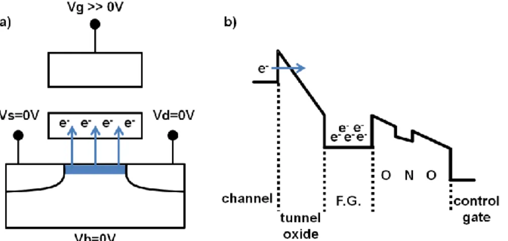
The Fowler-Nordheim programming operation is performed by applying a positive high voltage on the control gate terminal (about 20V) and keeping source drain and bulk grounded (figure 1.9a). The high electric field generated through the tunnel oxide creates a gate current due to the FN tunneling of charge from the channel to the floating gate [Chang '83].
19 Figure 1. 9. a) FN programming mechanism representation. b) Band diagram of a floating gate memory during
FN programming operation.
In this tunnel effect, the electrons flow from the conduction band of the silicon into the floating gate through the triangular energy barrier of the tunnel oxide (figure 1.9b). During the FN programming, the number of trapped electrons in the floating gate increases. As a consequence, the floating gate potential decreases and hence, the electric field through the tunnel oxide decreases. The charge injection will continue until the cancellation of electric field in the tunnel oxide. This is due to the maximum drop potential through the interpoly dielectric layer (ONO). This operation is relatively slow (order of milliseconds), but the energy consumption can be considered negligible because no current flows in the channel.
Channel Hot Electron programming
This operation is done keeping bulk and source grounded and applying a positive high voltage on gate (order of 10V) and drain (order of 5V) terminals (figure 1.10). The electrons are first strongly accelerated in the pinchoff region by the high lateral electric field induced by the drain/source bias. Then the electrons that have reached a sufficiently high kinetic energy are injected into the floating gate thanks to the vertical electric field induced by the positive voltage applied on the gate electrode [Ning '78] [Takeda '85] [Chenming '85]. Programming by channel hot electron is faster than FN (few microseconds). Furthermore the CHE is efficiency poor (only a few electrons are injected over the total amount of electrons that flow from source to drain [Simon '84]), and consequently high power consumption is reached. We remember that this programming mechanism is the main one used in this work to characterize the memory cells.
20 Figure 1. 10. Channel Hot Electron (CHE) programming mechanism representation.
1.3.3 Erase mechanisms
There are mainly four ways to erase the Flash floating gate cell; the schematic representations are shown in figure 1.11.
Figure 1. 11. Flash floating gate schematics of erase mechanisms: a) Fowler-Nordheim, b) Hot Hole Injection (HHI), c) source erasing, d) mix source-gate erasing.
21
Fowler-Nordheim erase
As for the programming operation, the source, drain and bulk are generally kept grounded while a strong negative voltage (order of -15V) is applied to the gate terminal. In this case, electrons are forced to flow from the floating gate to the semiconductor bulk. This method is slow, but the erasing is uniform on the channel surface (figure 1.11a). This is the preferred mechanism to erase the memory cells in NOR architecture. In the next chapter we will discuss about its effect on studied samples.
Hot Hole Injection (HHI) erase
This mechanism consists in accelerating the holes produced by reverse biasing of drain/bulk junction and by injecting them into the floating gate thanks to the vertical electric field [Takeda '83]. Figure 1.11b shows that this is done by keeping the bulk and source grounded and biasing positively the drain (order of 5V) and negatively the gate (about -10V). HHI erasing method is fast, localized near the drain and could induce the SILC (Stress Induced Leakage Current) phenomenon more easily than the methods listed above.
Source erasing
This forces electrons to flow from the floating gate into the source junction by FN tunneling. This erasing is done by applying a positive voltage of about 15V on the source and keeping bulk and gate grounded (figure 1.11c). In order to prevent current through the channel, the drain is kept floating. There are three main drawbacks to this method the erasing is localized near the source, it needs a strong source/gate overlap and it requires the application of a high voltage on the source terminal.
Mix source-gate erase
This is a mix between the source and the FN erasing. Electrons are erased both through the source and the channel. The principle is to share the high voltage needed in the source erasing between the gate and the source electrodes. As a result a negative bias of about -10V is applied on the gate and a positive bias of about 5V on the source. Again, the drain is kept floating in order to prevent source to drain current (figure 1.11d).
22
1.3.4 Evolution and limits of Flash memories
We explained at the beginning of the chapter that the new applications have commanded the semiconductor market and the research development. Since the invention of flash memory cell, the progress on device architectures and materials has been huge. The “ideal” memory should have:
• high density solution • low power consumption • non-volatility
• fast read/write/erase • random read/write access
• endurance against write/erase cycles • scalability with low cost
• compatibility with logic circuits and integration
This is the final objective of semiconductor research. As the “ideal” device does not exist different types of memories have been invented in order to push some specific properties. For these reasons, as shown in figure 1.12, memory technology development did not pursue a single technology solution, but rather it has oriented in many different direction over time [Hidaka '11] [Baker '12].
Figure 1. 12. Evolution of Flash and embedded-Flash memory technology (left) [Hidaka '11]. Mapping of common eNVM architectures to the NVM byte count and critical characteristics (right) [Baker '12].
Here, a category for non volatile storage with absolute minimum cost/bit is also shown. In this section we will first introduce the device scaling and the related challenges and then we will present flash cell developments. It is worth noting that the solutions found for the flash
23 memory cell can be used in embedded memory. In fact, even if in embedded memories there are minor constraints on the cell dimensions, research has always provided smaller non-volatile memory for embedded applications that have to face-off with the same flash scaling limits.
1.3.4.1 Device scaling
During the last 30 years Flash cell size has shrunk from 1.5um to 25nm doubling the memory capacity every year. In table 1.1 we report the international technology roadmap for semiconductor 2009 that forecasts the future trends of semiconductor technology.
ITRS 2012 - Process Integration, Devices, and Structures
2013 2016 2019 2022 2026
Nor flash technology node – F (nm) 45 38 32 28 22 ?
Cell size – area factor in multiplies of F2 12 12 12-14 14-16 14-16
Physical gate legth (nm) 110 100 90 85 85
Interpoli dielectric thickness (nm) 13-15 13-15 11-13 11-13 11-13
Table 1. 1. Table 1.1: Summary of the technological requirements for Flash NOR memories as stated in ITRS 2012 roadmap [ITRS '12]. White cell color: manufacturable solutions exist and are being optimized. Yellow cell
color: manufacturable solutions are known. Red cell color: unknown manufacturable solutions.
We can see that even if the trend is maintained and the cell scaled down in the years to come, some technological solutions are still not known. Moreover, scaling beyond the 28nm will be very difficult if no revolutionary technology is adopted. The main issues that limit device miniaturizing are:
Stress Induced Leakage Current (SILC). During each erase/write cycle the stress degrades
the tunnel oxide and the cell slowly loses its capacity to store electric charges (figure 1.13).
Figure 1. 13. Experimental cumulative distribution functions of bits vs. threshold voltage, measured at different times after different P/E cycling conditions[Hoefler '02].
24 This phenomenon, increases as the tunnel oxide is thinned. This is due to the defects induced in the oxide by the electrons that passing through it during program/erase operations [Pavan '97] [Ling-Chang '06] [Hoefler '02] [Belgal '02] [Kato '94] [Chimenton '01]. Consequently, the retention depends on the number of cycles and on the tunnel oxide thickness, but the physical scaling of this latter is limited to 6-7 nm.
Short Channel Effects (SCE). SCE appear when the gate length dimensions are so short that
the gate control of the channel is lowered due to the influence of the source and drain potentials (figure 1.14). This parasitic effect produces the Drain Induced Barrier Lowering (DIBL) phenomenon [Yau '75], which results in threshold voltage decrease and the degradation of the subthreshold slope. Because of DIBL, the "OFF" current (IOFF) increases
and the power consumption reaches values incompatible with the advanced technology node requirements [Brews '80] [Fichtner '80] [Yau '74] [Fukuma '77]. Moreover, elevated IOFF
currents result in some disturb of the memory cell, especially in the erased state.
Figure 1. 14. Subthreshold current of MOS transistor as a function of gate voltage with the channel length as parameter. The insert is the calculated boron profile below the silicon surface in the channel [Fichtner '80].
Disturb. We consider here the main disturb effects due to the programming and reading
operations done on unselected cell of a NOR memory array. It is to be remembered that in this thesis work, the electrical characterizations are based on the principle that the memory cells will be integrated in a NOR architecture for embedded applications.
Programming disturb. This impacts the unselected cells in the same bitline and wordline of selected cell. In the first case a drain stress is produced and the programmed cells can lose part of their charge due to FN drain stress on tunnel oxide causing hot hole injection (see the cell A in figure 1.15). The second case, represented in figure 1.15, cell B concerns a gate stress that can be induced on programmed cells (charge lost due to the stress through the ONO) or on erased cells (charge trapping due to the stress through the tunnel oxide).
25
Read disturb. In this case the selected cell can suffer from parasitic programming at low gate voltage; furthermore the unselected cells are gate stressed too (figure 1.15 cell C).
Figure 1. 15.Programming disturb (left) and read disturb (right) condition in NOR Flash memory array.
Coupling factor. As the cell dimensions are scaled down, the tunnel and interpoly dielectric
should be scaled accordingly. To maintain the gate coupling factor (αG) requirement, most
Flash structures have the word line (control gate) wrapped around the side-walls of the floating gate to increase the ONO capacitance (figure 1.16). However because the retention of the cell should remain higher than 10 years, the dielectrics have to scale at a slower rate. The cell scaling reduces the distances between the neighboring cells and the contacts. This means that parasitic capacitances have to be taken into account for the coupling factor calculation, and we will explain our model in chapter 4 section 2.2.
Figure 1. 16. TEM pictures of STMicroelectronics 90nm NOR Flash (left) and Samsung sub-50nm NAND Flash right) [Kim '05].
26
Parasitic Charge Trapping. In scaled memories the reduction in the number of stored
electrons leads to a higher influence of the parasitic charge trapping on threshold voltage shift [Prall '10]. Figure 1.17 shows various locations within a NAND cell, thus programmed and erased by FN, where the parasitic charge can be trapped. The results of a TCAD simulation show that with the memory scaling, the number of electrons located outside the floating gate starts to dominate the cell threshold voltage shift. We will see in following chapters, how this parameter impacts the memory cell behavior.
Figure 1. 17. Locations of parasitic charge in a NAND cell (left). Number of electrons required in each location to shift the cell VTH by 100mV (right) [Prall '10].
Random Doping Fluctuation. The threshold voltage shift due to random variations in the
quantity and position of doping atoms is an increasingly problem as device dimensions shrink. In figure 1.18 the mean and 3σ for the number of doping atoms are shown as a function of feature size. As device size scales down, the total number of doping atoms in the channel decreases, resulting in a larger variation of doping numbers, and significantly impacting threshold voltage. It has been documented [Frank '99] that at 25nm node, the Vt can be expected to vary of about 30% purely due to the random doping fluctuation.
Figure 1. 18. Number of Boron atoms per cell (mean: square, -3σ: diamond, +3σ: circle vs. feature size). The triangle shows the ±3σ percentage divided by the mean [Prall '10].
27
1.3.5 Alternative solutions
In this section we will describe some of the envisaged modification to the classical flash memory cell in order to overcome the scaling limits presented in the previous section.
1.3.5.1 Tunnel dielectric
In a flash memory the tunnel dielectric has the double role of tunneling media during programming operations and electrostatic barrier in order to preserve the stocked charge. Moreover we must avoid the creation of defects during the programming operations that can induce the SILC and degrade the retention and cycling performance. This technological challenge can be solved by engineering the tunnel barrier. As shown in figure 1.19 crested barriers can provide both sufficient programming and retention. Several crested barriers have been tested: the most common one consists in an ONO layer [Hang-Ting '05], but other combinations have also been experimented (SiO2/Al2O3/SiO2 [Blomme '09], SiO2/AlN
[Molas '10]).
Figure 1. 19. Principle of operation of crested barrier [Buckley '06].
1.3.5.2 Interpoly material
Maintaining a constant coupling ratio at a value of 0.6-0.7 is a great scaling challenge. The use of high-k dielectric in the interpoly dielectric is envisaged to reduce the total EOT while maintaining or even increasing the gate coupling ratio. The choice of the high-k must take into account that for most of them the high dielectric constant comes at the expense of a narrower band gap (figure 1.20). This narrowed band gap can cause leakage current during retention operation [Casperson '02]. In particular Alumina dielectric is employed in the TANOS (TaN/Al2O3/Si3N4/SiO2/Si) memory, proposed for the first time by Samsung in 2005 [Yoocheol '05], Despite the envisaged advantages, high-k materials are not as well known as the silicon oxide and they need further development before they can be integrated in the memory market. One of the main problems is that they inevitably introduce defects that can induce trap assisted conduction and degrade the memory operations [Leroux '04] [Wilk '01] [Ping-Hung '08].
28 Figure 1. 20. Relationship between the dielectric constant and band gap [Robertson '05].
1.3.5.3 Control Gate
During erasing operation, flash memories employing SiN as a charge trapping layer show a Vt saturation phenomenon (figure 1.21). This has been explained by the back-tunnelling effect. The back-tunnelling effect occurs during FN erasing operations when, due to the high negative bias applied on the gate electrode, the electrons flow from the poly-silicon gate to the charge trapping layer preventing the memory from completely erasing. To overcome this problem and in order to suppress the depletion capacitance of poly-silicon floating gate, different metallic materials with a high work function have been successfully tried improving erasing dynamic [Chang Hyun '03] .
Figure 1. 21. (a) Schematic explaining electron back tunneling phenomena. (b) Erase characteristics of SANOS device with n+ poly-Si gate and (c) TaN/n+ poly-Si gate.
1.3.5.4 Trapping layer
In figure 1.22a we show the schematics of continuous floating gate cell and discrete charge trapping layer. In the first case the trapped charge is free to move along the polysilicon floating gate. This makes the device very sensitive to SILC. A discrete charge trapping layer is the solution envisaged to avoid the charge loss if an electric path is generated in tunnel
29 oxide. Replacing of polysilicon layer by a discrete charge trapping layer (figure 1.20b) enables the localization of the stored charge that is not free to move, which reduces the impact of the SILC on data retention. In case of defect creation in tunnel oxide, only a part of the global stored charge can be lost. The most often used material for charge trapping layer is the silicon nitride (Si3N4). However other materials like HfSiON, AlN and Si, have also been
studied [Lai '05] [Wang '05] [Xuguang '04] [Monzio Compagnoni '04]. The subject of this thesis work is to characterize the silicon nanocrystal cell where the polysilicon charge trapping layer is replaced by silicon nanocrystals with and without the SiN capping layer. The results concerning the programming window, the reliability and the energy consumption will be shown in next chapters and compared to the standard floating gate.
Figure 1. 22. Schematic diagrams representing (SILC) phenomena for (a) continuous floating gate cell (b) discrete charge trapping layer.
1.4 Silicon nanocrystal memory: state of the art
The market of nonvolatile Flash memories, for portable systems, requires lower and lower energy and higher reliability solutions. The silicon nanocrystal Flash memory cell appears as one promising candidate for embedded applications. The functioning principle of discrete charge trapping silicon nanocrystal memories (Si-nc) is similar to floating gate devices. In this thesis we consider the integration of Si-nc memories in NOR architecture for embedded applications programmed by channel hot electron and erased by Fowler-Nordheim mechanisms.
There are many are the advantages to using this technology:
- Robustness against SILC and RILC (Radiation Induced Leakage Current), this enables to scale the tunnel oxide thickness to be scaled down to 5nm, while the ten year data retention constraint is guaranteed. Moreover the operation voltages can be decreased too [Compagnoni '03] [Monzio Compagnoni '04]. Further
30 improvements can be achieved using cells with a high number of nanocrystals [De Salvo '03].
- Full compatibility with standard CMOS fabrication process encouraging industrial manufacturability, reducing the number of masks with respect to the fabrication of floating gate device [Muralidhar '03] [Baron '04] and ease of integration [Jacob '08].
- Decrease in cell disturb, due to the discrete nature of nanocrystals and their smaller size than a floating gate, the coupling factor between the gate and drain is reduced as well as the disturbs between neighboring cells.
- Multi level applications, the threshold voltage of a silicon nanocrystal transistor depends on the position of stored charge along the channel [Crupi '03] [De Salvo '03].
Despite these peculiarities two main drawbacks characterize the Si-nc memories:
- The weak coupling factor between the control gate and nanocrystals. This implies finding a method to keep the program/erase voltages small and to take advantage of the decrease in tunnel oxide thickness [De Salvo '01].
- The spread in the surface fraction covered with Si-nc limiting this type of cell for high integration density applications [Gerardi '04].
IBM presented the first Si-nc memory at IEDM [Tiwari '95] in order to improve the DRAM (Dynamic Random Access Memory) performance using a device with characteristics similar to EEPROM. The polysilicon floating gate is replaced by silicon nanocrystals grown on tunnel oxide by Low Pressure Chemical Vapor Deposition (LPCVD) two step process. This type of fabrication enables the size and density of nanocrystals to be controlled separately [Mazen '03] [Mazen '04].
31 Other techniques of fabrication have also been developed: ionic implantation [Hanafi '96], annealing of SRO (Silicon Rich Oxide) layers deposition [Rosmeulen '02] and aereosol deposition [De Blauwe '00]. Thanks to these research works, Motorola demonstrated the interest in using this device for non-volatile applications by developing a 4Mb memory array [Muralidhar '03]. In addition STMicroelectronics in collaboration with CEA-Leti presented their 1Mb memory array [De Salvo '03]. The three main actors in the industry of silicon nanocrystal memories are STMicroelectronics, Atmel and Freescale.
STMicroelectronics, in collaboration with CEA-Leti, presented in 2003 a 1Mb nanocrystal
CAST (Cell Array Structure Test, figure 1.24a) where the Si-nc were fabricated with a two step LPCVD process [De Salvo '03] [Gerardi '04]. This structure is programmed and erased by Fowler-Nordheim tunneling, and the write/erase characteristics are reported in figure 1.24b.
Figure 1. 24. a) Schematic of a CAST structure. b) Program/erase characteristics in fully Fowler-Nordheim regime [De Salvo '03].
As a result STMicroelectronics presented in 2007 a 16Mb Flash NOR memory array divided into 32 sectors of 512kb [Gerardi '07a] [Gerardi '07b]. The silicon nanocrystals were grown on a tunnel oxide, 5nm thick, with a diameter between 3nm and 6nm and a density of 5·1011nc/cm2. To complete the stack an ONO layer was used as a control oxide (EOT=12nm).
In figure 1.25a the program/erase threshold voltage distributions of 16Mb memory array are plotted. In this case the cells have been programmed by channel hot electron and erased by Fowler-Nordheim reaching a 3V programming window in case of the average of distributions and 800mV for the worst case. Moreover Gerardi highlighted the problem of parasitic charge trapping in ONO layer during the cycling (figure 1.25b).
32 Figure 1. 25. a) Program and erase threshold voltage distributions for one sector of 512 kb of nanocrystal memory cells. b) Evolution of the program/erase threshold voltages of a Si-nc memory cell showing that the
program/erase levels are shifted due to electron trapping in the ONO [Gerardi '07b].
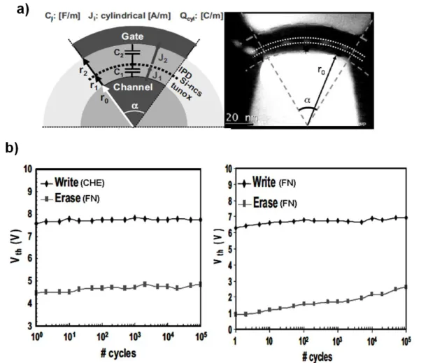
Finally they processed the silicon nanocrystal memory cell in order to assume a cylindrical shape, which greatly benefits improve the coupling ratio (figure 1.26a). In addition, they used an optimized ONO control dielectric, enabling the reduction of the parasitic charge trapping during cycling (figure 1.26b); this type of cell was integrated in a 4Mb NOR array [Gerardi '08].
Figure 1. 26. a) Cross-section of the cylindrical-shaped structure and corresponding TEM image on the right. b) Endurance characteristic of a Si-nc cell by using CHE/FN and FN/FN program/erase operations.
33
ATMEL presented an extensive set of experiments, resulting from a joint venture with
CEA-Leti. In this context, they demonstrated the validity of the discrete storage node concept on a 32Mb Si-NC NOR Flash memory product, fabricated in a 130 nm technology platform. The presented results gave a quantitative estimation of the maturity of two step LPCVD Si-NC technology [Jacob '07]. Their study focused on the impact of silicon nanocrystal size on memory cell performance integrating a HTO (High Temperature Oxide) as control oxide in order to avoid the parasitic charge trapping in ONO layer shown by STMicroelectronics results. In figure 1.27b the written and erased threshold voltages, measured on a set of 40 memory cells, are shown (corresponding to different dot sizes, see figure 1.27a) [Jacob '08].
Figure 1. 27. a) SEM images of Si-NCs with same dot nucleation step and different dot growing times. b) written and erased Vth of bitcells with different Si-NCs [Jacob '08].
It clearly appears that increasing the Si-nc size, the programming window is increased too. Indeed, this result well agrees with the theoretical model [De Salvo '01] which states that the programming window linearly increases with the floating gate surface portion covered by the Si-NCs. In fact it was demonstrated for the Si-nc cell that the dynamic charging/discharging Si-dot memory corresponds better to a FG memory device operation rather than to a pure capture/emission trap-like behavior [De Salvo '01]. Starting from the capacitive model of
34 Flash floating gate (section 1.3.1), and by considering the discrete nature of nanocrystals, the coefficient αD can be neglected and the equation (8) can be rearranged as:
T G G FG C Q V V (10)
In this FG-like approach, we define a parameter that takes into account the surface portion covered by the nanocrystals (Rnc). It corresponds to a weighting factor for the trapped charges
in the MOSFET threshold voltage; the Vt shift in this case takes into account this parameter and can be written as:
FC nc C R Q Vt Vt Vt 0 (11)
This approach will be considered as fundamental in the next chapters in order to improve the Si-nc memory cell coupling factor and thus the programming window.
We reported in figure 1.28 the results shown in [Jacob '08] concerning cell reliability using the HTO control oxide and keeping the silicon nanocrystal size constant.
Figure 1. 28. a) Endurance data for a memory bitcell b) Threshold voltage distributions of erased and written states of two different sectors, measured before and after 10k write/erase cycles. c) Data retention at 150°C on
35 Figure 1.28a shows the program/erase endurance data of a memory bitcell corresponding to a sample with 9nm Si-nc diameter and 1012nc/cm² Si-nc density. The cell has been
programmed by CHE adding a substrate biasing that enables trapping charge in the nanocrystals positioned toward the center of channel; this improves the programming window but degrades the analog circuit area and the cell consumption. The initial programming window (larger than 4V) decreases to 3V after 100kcycles, showing that even if the ONO layer is substituted by the HTO a parasitic charge trapping occurs. This appears also in figure 1.28b where the threshold voltage distributions of erased and programmed states of two different sectors are shown, measured before and after 10k write/erase cycles. In this case the programming window of tail bits is 600mV. To conclude, the data retention is reported in figure 1.28c. At 150°C the programming window loses 500mV after 168h.
Freescale was created by Motorola in 2004 when the studies on silicon nanocrystal memory
cell had already been started [Muralidhar '03]. Freescale did a comparative study on the importance of control dielectric, using HTO and ONO samples because the latter, with its silicon nitride layer, represents a barrier against the parasitic oxidation of silicon nanocrystals and decreases the leakage current in the memory stack. As a drawback the parasitic charge trapping is present during the programming operations. In figure 1.29 we report the endurance characteristics of HTO and ONO samples fabricated by Freescale. For the HTO sample the threshold voltages remain stable up to 1kcycles, and afterwards their increase is explained by the parasitic charge trapping in the oxide. In the case of ONO sample, the electrons trapping in the silicon nitride layer starts immediately with the first program/erase cycles figure 1.29.
Figure 1. 29. Endurance characteristics of silicon nanocrystal cells integrating a) HTO [Steimle '04] and b) ONO [Muralidhar '04] control dielectric.
36 This parasitic charge trapping impacts also the data retention (figure 1.30). It is thus important to minimize it to reach the 20 year target. They demonstrated the advantage of discrete nature of silicon nanocrystals on data retention and read disturb; it enables the tunnel oxide thickness to be decreased and hence the program/erase voltages.
Figure 1. 30. Program state data retention and erased slate READ disturb characteristics for a nanocrystal NVM bitcell with a 5mn tunnel oxide. Exhibited charge loss in cycled case is attributed to detrapping of
parasitic charge [Muralidhar '04].
Further studies have been performed concerning the impact of silicon nanocrystals size and density [Rao '05] [Gasquet '06]. Figure 1.31a shows that the covered area impacts the program/erase speed and the saturation level of the programming window.
Figure 1. 31. a) HCI program and FN erase speed (with positive gate voltage) for devices with 4.5nm bottom oxide and 12nm top oxide, with different nanocrystal depositions [Rao '05]. b) 200ºC bake Vt shift for samples
37 The hot carrier injection speed increases with the covered area, while the Fowler-Nordheim erase operation is more efficient with smaller nanocrystals. This is due to the presence of HTO and the Coulomb blockade effect. Data retention measurements have been also carried out on a 4Mb memory array. The samples had a 5nm tunnel oxide and 10nm HTO (figure 1.31b). Here the data retention loss is shown during a 200ºC bake. The erased state is very close to neutral charge so the Vt shift is small while most of the variation in program state response originates in the first 54 hours of bake and appear uncorrelated to nanocrystal size. Moreover, Freescale decided to integrate silicon nanocrystals in high scalable Split Gate memories (figure 1.32) [Sung-Taeg '08] [Yater '09], where it is possible to control the current consumption during the hot carrier injection for low energy embedded applications [Masoero '11] [Masoero '12b].
Figure 1. 32. Schematic of Split Gate with memory first Left) or Access first (Right) configuration [Masoero '12a].
Recent results of endurance and data retention are reported in figure 1.33.
Figure 1. 33. a) Erase and program Vt distributions of cycles up to 300K at 25°C. b) Bake retention characteristics at 150C with fresh, 10K and 100K cycled parts of 125°C cycling temperature [Sung-Taeg '12].
38 The cycling experiments (figure 1.33a) show program and erase Vt distribution width that remain approximately constant throughout extended cycling and a substantial operating window is maintained even after 300Kcycles. Concerning the data retention, due to the inherent benefits of NC-based memories, no extrinsic charge loss was observed on fresh and cycled parts (figure 1.33b). The average loss for 504hrs for uncycled arrays is about 70mV and for 10K and 100K cycled arrays it is 250mV and 400mV, respectively [Yater '11] [Sung-Taeg '12]. Finally all these studies underline the importance of achieving a good coupling factor to improve the programming window and thus cell endurance, paying attention to the tunnel oxide thickness that plays an important role for the data retention and disturbs.
1.5 Flash technology for embedded applications
The 1T silicon nanocrystal technology is not the only solution to replace the Flash floating gate. In particular for the market of embedded applications the Flash memory array is integrated in the microcontroller products with SRAM, ROM and logic circuits achieving System on a Chip solution (SoC). This type of integrated circuit enables the fabrication costs reduction due to the compatibility with the CMOS process, by improving the system performance because the code can be executed directly from the embedded Flash. The most important applications for embedded products are the smart card and automotive, where low energy consumption, fast access time and high reliability are required (figure 1.34). In this scenario each one of main industrial actors searches the best compromise between cell area, performance and cost. In figure 1.35 we show the mainstream Flash concepts proposed by the top players of SoC manufacturers [Strenz '11].
39 Figure 1. 35. Mainstream Flash integration concept [Strenz '11].
Although a large variety of different cell concepts can be found in sell, only three main concepts in terms of bitcell structure dominate the market – all of them using NOR array configuration: 1T stacked gate concepts, splitgate concepts as well as 2-transistor NOR concepts. Due to highly diverging product requirements there is a variety of concepts tailored to specific applications. Looking into development of new nodes a clear slowdown of area shrink potential can be observed for classical bitcell concepts while reliability requirements are tightened rather than relaxed. This increases the pressure for new, emerging cell concepts with better shrink potential. We used this brief analysis (Robert Strenz, Infineon - Workshop on Innovative Memory Technologies, Grenoble 2012), to highlight the concept that the industry push its technology to overcome the problem of scaling cost.
1.6 Innovative solutions for non volatile memory
Since the ultimate scaling limitation for charge storage devices is too few electrons, devices that provide memory states without electric charges are promising to scale further. Several non-charge-storage memories have been extensively studied and some commercialized, and each has its own merits and unique challenges. Some of these are uniquely suited for special applications and may follow a scaling path independent of NOR and NAND flash. Some may eventually replace NOR or NAND flash. Logic states that do not depend on charge storage eventually also run into fundamental physical limits. For example, small storage volume may be vulnerable to random thermal noise, such as the case of superparamagnetism limitation for MRAM. One disadvantage of this category of devices is that the storage element itself cannot
40 also serve as the memory selection (access) device because they are mostly two-terminal devices. Even if the on/off ratio is high, two terminal devices still lack a separate control (e.g. gate) that can turn the device off in normal state. Therefore, these devices use 1T-1C (FeRAM), 1T-1R (MRAM and PCRAM) or 1D-1R (PCRAM) structures. It is thus challenging to achieve small (4F2) cell size without an innovative access device. In addition,
because of the more complex cell structure that must include a separate access (selection) device, it is more difficult to design 3-D arrays that can be fabricated using just a few additional masks like those proposed for 3-D NAND [ITRS '12] [Jiyoung '09] [Tae-Su '09] [SungJin '10] [Eun-Seok '11] (figure 1.36).
Figure 1. 36. An overview on 3D array integration of charge trapped Flash NAND: a) [Jiyoung '09], b)[Tae-Su '09], c) [SungJin '10], d) [Eun-Seok '11].
1.6.1 Ferroelectric Random Access Memory (FeRAM)
FeRAM devices achieve non-volatility by switching and sensing the polarization state of a ferroelectric capacitor. To read the memory state the hysteresis loop of the ferroelectric capacitor must be traced and the data must be written back after reading. Because of this “destructive read,” it is a challenge to find ferroelectric and electrode materials that provide both adequate change in polarization and the necessary stability over extended operating cycles. The ferroelectric materials are foreign to the normal complement of CMOS fabrication materials and can be degraded by conventional CMOS processing conditions. Thus, the ferroelectric materials, buffer materials and process conditions are still being refined. So far, the most advanced FeRAM [Hong '07] is substantially less dense than NOR
41 and NAND flash. It is fabricated at least one technology generation behind NOR and NAND flash, and not capable of MLC. Thus, the hope for near term replacement of NOR or NAND flash has faded. However, FeRAM is fast, low power and low voltage, which makes it suitable for RFID, smart card, ID card and other embedded applications. In order to achieve density goals with further scaling, the basic geometry of the cell must be modified while maintaining the desired isolation. Recent progress in electrode materials show promise to thin down the ferroelectric capacitor [ITRS '12] and extend the viability of 2-D stacked capacitor through most of the near-term years. Beyond this the need for 3-D capacitors still remains a formidable challenge.
1.6.2 Magnetic Random Access Memory (MRAM)
MRAM devices employ a magnetic tunnel junction (MTJ) as the memory element. An MTJ cell consists of two ferromagnetic materials separated by a thin insulating layer that acts as a tunnel barrier. When the magnetic moment of one layer is switched to align with the other layer (or to oppose the direction of the other layer) the effective resistance to current flow through the MTJ changes. The magnitude of the tunneling current can be read to indicate whether a ONE or a ZERO is stored. Field switching MRAM probably is the closest to an ideal “universal memory”, since it is non-volatile and fast and can be cycled indefinitely, thus may be used as NVM as well as SRAM and DRAM. However, producing magnetic field in an IC circuit is both difficult and inefficient. Nevertheless, field switching MTJ MRAM has successfully been done in products. In the near term, the challenge will be the achievement of adequate magnetic intensity fields to accomplish switching in scaled cells, where electromigration limits the current density that can be used. Therefore, it is expected that field switch MTJ MRAM is unlikely to scale beyond 65 nm node. Recent advances in “spin-torque transfer (STT)” approach, where a spin-polarized current transfers its angular momentum to the free magnetic layer and thus reverses its polarity without resorting to an external magnetic field, offer a new potential solution [Miura '07]. During the spin transfer process, substantial current passes through the MTJ tunnel layer and this stress may reduce the writing endurance. Upon further scaling the stability of the storage element is subject to thermal noise, thus perpendicular magnetization materials are projected to be needed at 32 nm and below [ITRS '12].
![Figure 1. 24. a) Schematic of a CAST structure. b) Program/erase characteristics in fully Fowler-Nordheim regime [De Salvo '03]](https://thumb-eu.123doks.com/thumbv2/123doknet/14663906.740265/36.893.127.773.509.787/figure-schematic-structure-program-characteristics-fowler-nordheim-regime.webp)
![Figure 1. 29. Endurance characteristics of silicon nanocrystal cells integrating a) HTO [Steimle '04] and b) ONO [Muralidhar '04] control dielectric](https://thumb-eu.123doks.com/thumbv2/123doknet/14663906.740265/40.893.168.731.826.1104/figure-endurance-characteristics-nanocrystal-integrating-steimle-muralidhar-dielectric.webp)
![Figure 1. 31. a) HCI program and FN erase speed (with positive gate voltage) for devices with 4.5nm bottom oxide and 12nm top oxide, with different nanocrystal depositions [Rao '05]](https://thumb-eu.123doks.com/thumbv2/123doknet/14663906.740265/41.893.225.689.664.1086/figure-program-positive-voltage-devices-different-nanocrystal-depositions.webp)