Publisher’s version / Version de l'éditeur:
Analytical Chemistry, 80, 13, pp. 4945-4950, 2008-05-29
READ THESE TERMS AND CONDITIONS CAREFULLY BEFORE USING THIS WEBSITE. https://nrc-publications.canada.ca/eng/copyright
Vous avez des questions? Nous pouvons vous aider. Pour communiquer directement avec un auteur, consultez la première page de la revue dans laquelle son article a été publié afin de trouver ses coordonnées. Si vous n’arrivez pas à les repérer, communiquez avec nous à PublicationsArchive-ArchivesPublications@nrc-cnrc.gc.ca.
Questions? Contact the NRC Publications Archive team at
PublicationsArchive-ArchivesPublications@nrc-cnrc.gc.ca. If you wish to email the authors directly, please see the first page of the publication for their contact information.
NRC Publications Archive
Archives des publications du CNRC
This publication could be one of several versions: author’s original, accepted manuscript or the publisher’s version. / La version de cette publication peut être l’une des suivantes : la version prépublication de l’auteur, la version acceptée du manuscrit ou la version de l’éditeur.
For the publisher’s version, please access the DOI link below./ Pour consulter la version de l’éditeur, utilisez le lien DOI ci-dessous.
https://doi.org/10.1021/ac800149d
Access and use of this website and the material on it are subject to the Terms and Conditions set forth at
Multiple surface plasmon resonances and near-infrared field
enhancement of gold nanowells
Li, Kebin; Clime, Liviu; Tay, Lilin; Cui, Bo; Geissler, Matthias; Veres, Teodor
https://publications-cnrc.canada.ca/fra/droits
L’accès à ce site Web et l’utilisation de son contenu sont assujettis aux conditions présentées dans le site
LISEZ CES CONDITIONS ATTENTIVEMENT AVANT D’UTILISER CE SITE WEB.
NRC Publications Record / Notice d'Archives des publications de CNRC:
https://nrc-publications.canada.ca/eng/view/object/?id=1cd10865-b317-448e-b4e4-a842f4d8d265
https://publications-cnrc.canada.ca/fra/voir/objet/?id=1cd10865-b317-448e-b4e4-a842f4d8d265
Multiple Surface Plasmon Resonances and
Near-Infrared Field Enhancement of Gold
Nanowells
Kebin Li,*,†Liviu Clime,†Lilin Tay,‡Bo Cui,†Matthias Geissler,†and Teodor Veres†
Industrial Materials Institute, National Research Council Canada, 75 de Mortagne, Boucherville, Que´bec, J4B 6Y4, Canada, and Institute for Microstructural Sciences, National Research Council Canada, 1200 Montreal Road, Ottawa, Ontario K1A 0R6, Canada
Arrays of Au nanowells (NWs) were fabricated by electron-beam lithography (EBL) and characterized by surface plasmon resonance (SPR) and surface-enhanced Raman scattering (SERS). It is revealed that these Au NW arrays exhibit multiple SP resonances that can be tuned by adjusting the geometrical characteristics of the NWs. SERS activity of Au NWs was confirmed for a range of excitation wavelengths and a number of model com-pounds including rhodamine 6G (R6G), phthalazine, and single-stranded oligonucleotides. According to numerical simulations based on the discrete dipole approximation (DDA), SERS enhancement originates from high electro-magnetic fields (hot spots) localized both inside and outside individual NWs. In addition, far-field intercou-pling effects between NWs have been observed experi-mentally in arrays with subwavelength pitch sizes. We show that the SERS enhancement factors can also be tuned and optimized by adjusting the geometry of NWs.
The interaction between light and metallic nanostructures can lead to interesting charge-density excitations and unique electro-magnetic effects, including surface plasmons (SP) and surface plasmon resonance (SPR).1–3Over the past decade, SP effects
have experienced increasing attention due to their fundamental and practical significance.4,5From a fundamental point of view,
SPs play an important role for scientists in unveiling the physical interaction between light and matter at the nanoscale level. Practically, SPs are being explored for their potential in optical signal processing,6–8magneto-optic data storage,9,10solar cells,11
plasmonic devices,12–15as well as sensors for detecting
biomol-ecules.16–28Surface plasmon resonance spectroscopy and
surface-enhanced Raman scattering (SERS) are two effects in which localized SPs can be used for the detection of chemical and biological species. Since its discovery,29,30SERS has proven to
be a sensitive technique able to detect a single molecule.31,32Its
chemical specificity and label-free nature have enabled many analytical, biomedical, or environmental applications, potentially improving global and homeland security domains.33 It is
well-known that the large signal enhancements in SERS mainly originate from excitation of localized SPR in metallic nanostruc-tures.34Various types of nanostructures including Au nanodisc
arrays,35bowtie nanoantennas,36nanoburgers,37triangular
nano-* To whom correspondence should be addressed. E-mail: kebin.li@ cnrc-nrc.gc.ca.
†Industrial Materials Institute. ‡
Institute for Microstructural Sciences.
(1) Ho¨vel, H.; Fritz, S.; Hilger, A.; Kreibig, U.; Vo¨llmer, M. Phys. Rev. B 1993,
48, 18178.
(2) Kreibig, U.; Vo¨llmer, M. Optical Properties of Metal Clusters; Springer-Verlag: Berlin, 1995.
(3) Ritchie, R. H. Phys. Rev. 1957, 106, 874.
(4) Barnes, L.; Dereux, A.; Ebbesen, T. W. Nature 2003, 424, 824. (5) Stuart, D. A.; Haes, A. J.; Yonzon, C. R.; Hicks, E. M.; Van Duyne, R. P.
IEE Proc.: Nanobiotechnol.2005, 152, 13.
(6) Sambles, J. R.; Bradbery, G. W.; Yang, F. Z. Contemp. Phys. 1991, 32, 173.
(7) Smolyaninov, I. I. Phys. Rev. Lett. 2005, 94, 057403.
(8) Wurtz, G. A.; Pollard, R.; Zayats, A. V. Phys. Rev. Lett. 2006, 97, 057402.
(9) Bonod, N.; Reinisch, R.; Popov, E.; Nevie`re, M. J. Opt. Soc. Am. B 2004,
21, 791.
(10) Nevie`re, M.; Popov, E.; Reinisch, R.; Vitrant, G. Electromagnetic Resonances
in Nonlinear Optics; Gordon and Breach: London, 2000.
(11) Derkacs, D.; Lim, S. H.; Matheu, P.; Mar, W.; Yu, E. T. Appl. Phys. Lett.
2006, 89, 093103.
(12) Andersen, P. C.; Rowlen, K. L. Appl. Spectrosc. 2002, 7, 124A. (13) Maier, S. A.; Brongersma, M. L.; Kik, P. G.; Meltzer, S.; Requicha, A. A. G.;
Atwater, H. A. Adv. Mater. 2001, 13, 1501.
(14) Maier, S. A.; Kik, P. G.; Atwater, H. A.; Meltzer, S.; Harel, E.; Koel, B. E.; Requicha, A. A. G. Nat. Mater. 2003, 2, 229.
(15) Shelby, R. A.; Smith, D. R.; Schultz, S. Science 2001, 292, 77. (16) Aizpurua, J.; Hanarp, P.; Sutherland, D. S.; Ka¨ll, M.; Bryant, G. W.; García
de Abajo, F. J. Phys. Rev. Lett. 2003, 90, 057401–1.
(17) Bailey, R. C.; Nam, J.-M.; Mirkin, C. A.; Hupp, J. T. J. Am. Chem. Soc. 2003,
125, 13541.
(18) Fritzsche, W.; Taton, T. A. Nanotechnology 2003, 14, R63.
(19) Haes, A. J.; Van Duyne, R. P. J. Am. Chem. Soc. 2002, 124, 10596. (20) Haes, A. J.; Van Duyne, R. P. Laser Focus World 2003, 39, 153.
(21) Hirsch, L. R.; Jackson, J. B.; Lee, A.; Halas, N. J.; West, J. L. Anal. Chem.
2003, 75, 2377.
(22) Homola, J.; Yee, S. S.; Gauglitz, G. Sens. Actuators, B 1999, 54, 3. (23) Mucic, R. C.; Storhoff, J. J.; Mirkin, C. A.; Letsinger, R. L. J. Am. Chem.
Soc.1998, 120, 12674.
(24) Nam, J.-M.; Thaxton, C. S.; Mirkin, C. A. Science 2003, 301, 1884.
(25) Nath, N.; Chilkoti, A. Proc. SPIEsInt. Soc. Opt. Eng. 2002, 4626, 441. (26) Obare, S. O.; Hollowell, R. E.; Murphy, C. J. Langmuir 2002, 18, 10407.
(27) Riboh, J. C.; Haes, A. J.; McFarland, A. D.; Yonzon, C. R.; Van Duyne, R. P.
J. Phys. Chem. B2003, 107, 1772.
(28) Chen, J.; Saeki, F.; Wiley, B. J.; Cang, H.; Cobb, M. J.; Li, Z. Y.; Au, L.; Zhang, H.; Kimmey, M. B.; Li, X.; Xia, Y. Nano Lett. 2005, 5, 473.
(29) Fleischmann, M.; Hendra, P. J.; McQuillan, A. J. Chem. Phys. Lett. 1974,
26, 163.
(30) Jeanmaire, D. J.; Van Duyne, R. P. J. Electroanal. Chem. 1977, 84, 1. (31) Kneipp, K.; Wang, Y.; Kneipp, H.; Perelman, L. T.; Itzkan, I.; Dasari, R. R.;
Feld, M. S. Phys. Rev. Lett. 1997, 78, 1667. (32) Nie, S. M.; Emory, S. R. Science 1997, 275, 1102.
(33) Baker, G. A.; Moore, D. S. Anal. Bioanal. Chem. 2005, 382, 1751. (34) Moskovits, M. Rev. Mod. Phys. 1985, 57, 783.
(35) Qin, L.; Zou, S.; Xue, C.; Atkinson, A.; Schatz, G. C.; Mirkin, C. A. Proc.
Natl. Acad. Sci. U.S.A.2006, 103, 13300.
Anal. Chem. 2008, 80, 4945–4950
prisms,38and nanopins39have been suggested for inducing local
enhancement of electromagnetic fields. Moreover, both SPR and SERS effects have been integrated into microfluidic chips for accurate and precise analysis of biological species such as DNA labeled with a fluorescent dye.40However, visible excitation laser
sources commonly used in SERS experiments can cause photo-chemical reactions on the surface as well as fluorescence from the adsorbed molecules. A way to circumvent this difficulty is to use near-infrared (NIR) laser sources. It is therefore desirable to tune the SPR frequencies of the substrate to the NIR regime to optimize SERS enhancement. Recently, Mahajan et al.41have used
spheres of various sizes in colloidal templates and electrochemical control over the film height to optimize SERS-active substrates in the NIR regime for molecules of a particular probe. It has also been demonstrated that ringlike nanoparticles exhibit tunable plasmon resonances by tailoring their aspect ratio16and extinction
maxima in the NIR.42In this paper, we report on the design,
fabrication, and characterization of the SPR and SERS effects on electron-beam lithography (EBL) fabricated periodic arrays of Au nanowells (NW). We analyze the SPR spectra and the near-field enhancement around individual Au NWs of different geometries and explain the origin of the experimentally observed SERS enhancement. The geometrical parameters responsible for tuning the SPR absorption peaks in the NIR regime and the localization of the regions of high field concentrations (hot spots) are discussed as well.
EXPERIMENTAL SECTION
Fabrication of Au NWs Substrates. The fabrication process of the NW arrays used in the present study is summarized below: (1) arrays of nanoring patterns with different pitches and dimen-sions were created by using EBL (Hitachi S4800 installed with a Nabity NPGS system) on poly(methyl methacrylate) (PMMA, 950K, MICRO-CHEM) resist using a beam energy of 30 keV, a writing current of 30 pA, and an exposure dose of 2 nC/cm; (2) a 20 nm thick Cr nanoring was obtained by standard Cr deposition and lift-off process; (3) by using reactive ion etching (RIE) to transfer the Cr nanorings to the Si wafer, Si NWs are formed after the Cr removal by using a commercial Cr etchant (CR-4S); (4) arrays of Au NWs are finally obtained by evaporation of gold at normal incidence on the nanostructures previously generated on the Si substrate. Each NW consists of a Au disk inside a hollow Si cylinder and a Au donut on top of this cylinder.
Immobilization of Probes. Rhodamine 6G (R6G, Sigma-Aldrich) with a concentration of 1 × 10⁻³ M was obtained by
dissolving 47.5 mg of R6G powder into 100 mL of deionized (DI) water. Aqueous R6G solutions with other concentrations are then obtained by further dilutions of this initial solution in DI water.
Au NW substrates were incubated with R6G solutions for ∼1 h and dried with a stream of N2gas. For adsorption of phthalazine, a 0.1 mM aqueous solution was applied to a Au NW substrate for ∼4 h, followed by a rigorous rinse with DI water and drying with a stream of N2gas. Oligonucleotides 1 (5′-Cy3-CGG GCA GCA TCA AGC-(CH2)6-NH2-3′) and 2 (5′-ACC GAT GTT TCT ACC TGC AC-(CH2)6-NH2-3′) were purchased from Integrated DNA Technologies, Inc. and used without further purification. For covalent attachment of DNA molecules, Au NWs were exposed to a 2 mM solution of 11-mercaptoundecanoic acid (Sigma-Aldrich) in methanol for 1 h, rinsed with methanol, and dried with a stream of N2gas. The modified sample was then incubated with a 50 µM solution of oligonucleotide 1 in phosphate-buffered saline (PBS, pH 7.4, Sigma-Aldrich) containing 0.2 mg of N-hydroxysuccinimide (NHS, Sigma-Aldrich) and 0.8 mg of 1-ethyl-3-(3-dimethylamino-propyl)carbodiimide hydrochloride (EDC, Sigma-Aldrich) for ∼12 h. The sample was stored in a sealed Petri dish (Sigma-Aldrich) containing an excess of DI water to limit evaporation and prevent drying of the DNA solution. The substrate was rinsed with DI water to remove nonspecifically adsorbed DNA molecules followed by drying with a stream of N2gas. Oligonucleotide 2 was physically adsorbed on the surface of Au NWs through incubation with a 10 µM aqueous solution for ∼12 h, followed by rinsing with DI water and drying with a stream of N2gas.
Raman Spectroscopy. Raman spectra were acquired by using a LabRam HR from Horiba Jobin Yvon with multiple excitation sources. The spectra were collected by using a 100× objective lens for 3 s with a spot diameter of about 1 µm and power of 0.1 mW at λ ) 633 nm and 1.1 mW at λ ) 785 nm, 0.4 mW at λ ) 488 nm. Some of the Raman spectra were acquired with a 40× objective lens coupled to a Raman Micro Station R3 (Avalon Instruments) operating at λ ) 785 nm. The spot size and power density of the laser were 25 µm and 0.15 mW/µm2, respectively.
All spectra were calibrated with respect to the Raman peak of Si at 520 cm-1.
UV-Vis Spectroscopy. UV-vis spectra were measured with a microspectrophotometer (QDI 2010, CRAIC Technologies) operated in reflection mode. The system was equipped with a 50 W xenon light source and a linear Si array detector. All measure-ments were done with a 36×all-reflective objective lens, and the acquired spectra were referenced to the bare Au film in the unpatterned area.
RESULTS AND DISCUSSION
Figure 1 shows typical scanning electron microscope (SEM) images at different stages in the fabrication of Au NW arrays by the above-described method. The NWs we employed for this study consisted of a hollow Si cylinder with a Au nanodisc at the bottom of its interior and a Au nanodonut on top of it. The nanodisc and the nanodonut are weakly coupled by a discontinuous layer of small Au particles with diameters up to 10 nm coated on the walls inside each well. Nanodonuts are equally coupled with the base of the continuous Au film by a similar layer coated on the external wall of the well. The thickness of both the Au nanodisc and nanodonut was about 25 nm, whereas the vertical distance between them was about 100 nm. The geometry of the NW can be therefore described by two parameters, namely, the inner diameter (Di) and the outer diameter (Do) of the donut, while the thickness of both the nanodisc and nanodonut as well as the height
(36) Ja¨ckel, F.; Kinkhabwala, A. A.; Moerner, W. E. Chem. Phys. Lett. 2007,
446, 339.
(37) Su, K.; Durant, S.; Steele, J. M.; Xiong, Y.; Sun, C.; Zhang, X. J. Phys. Chem.
B2006, 110, 3964.
(38) Jensen, T. R.; Malinsky, M. D.; Haynes, C. L.; Van Duyne, R. P. J. Phys.
Chem. B2000, 104, 10549.
(39) Wang, S.; Pile, D. F. P.; Sun, C.; Zhang, X. Nano Lett. 2007, 7, 1076.
(40) Docherty, F. T.; Monaghan, P. B.; Kier, R.; Graham, D.; Smith, W. E.; Cooper, J. M. Chem. Commun. 2004, 118.
(41) Mahajan, S.; Abdelsalam, M.; Suguwara, Y.; Cintra, S.; Russell, A.; Baum-berg, J.; Bartlett, P. Phys. Chem. Chem. Phys. 2007, 9, 104.
(42) Larsson, E. M.; Alegret, J.; Ka¨ll, M.; Sutherland, D. S. Nano Lett. 2007, 7, 1256.
of the Si cylinder remained constant. The diameter of each nanodisc is approximately the same as Diof the Si cylinder.
We have fabricated two batches of NW arrays for studying the effect of aspect ratio and the coupling among individual NWs and another two batches of NW arrays for their application in DNA detection. Each batch consisted of eight dies with differences in
Do, Di, and pitch (P) as shown in Table 1. The overall area of each die was about 80 × 80 µm2. The distance between two
adjacent dies was 240 µm, large enough to avoid interference during the measurements of UV-vis reflective spectra.
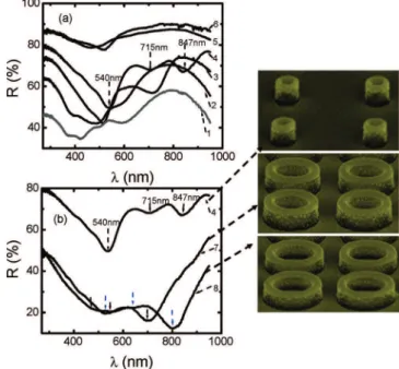
Figure 2 shows the experimental UV-vis diffusive reflectance spectra acquired on eight dies of Au NWs (Table 1). As shown in Figure 2a, the reflectance of the NW arrays decreases as the area density of NWs increases (the value of P is reduced from 800 to 300 nm). Moreover, the reflectance decreases with increasing the NW diameter when P is kept around 600 nm, as shown in Figure 2b. There are three apparent diffusive peaks located at 540, 715, and 847 nm for the Au NWs of Di) 50 nm, Do) 180 nm, and P ) 600 nm (curve 4 in Figure 2). The peak at 540 nm is associated with the continuous Au base film. However, compared to the continuous Au film (in the nonpatterned area) a red-shift of about 50 nm was observed (data not shown). The peaks located at 715 and 847 nm are associated with the NWs, the former being attributed to the nanodisc and the latter to the nanodonut. The position of all three peaks can be tuned by varying both the geometry of the NW and pitch of the array. This finding indicates that in addition to the interactions between discs and donuts in individual NWs, there are mutual intercoupling effects between
individual NWs as well as between NWs and the base of the Au thin film. However, these effects become negligible for P > 700 nm .
The spectra in Figure 2a further indicate that it was possible to shift one of the SPR peaks to the NIR regime. This peak is associated with the SPR characteristics of the nanodonuts which are somewhat similar to those of Au nanorings reported by Aizpurua et al.16According to this reference, the position of this
peak depends on the ratio r of the wall thickness and radius. We therefore conclude that the global shift of this NIR peak originates from a combined effect, involving the variation in r on the one
Figure 1.SEM images of nanostructures at different fabrication stages. (a-c) Cr nanorings on a Si substrate after lift-off. (d-f) Au NWs formed by deposition of 25 nm of Au onto the corresponding substrates. Features were observed at a tilt angle of 60°.
Table 1. Geometrical Parameters Do, Di, and P for the
Dies Used in this Study
die Do(nm) Di(nm) P (nm) 1 180 50 300 2 180 50 400 3 180 50 500 4 180 50 600 5 180 50 700 6 180 50 800 7 375 239 500 8 492 320 620
Figure 2.(a) UV-vis spectra of Au NWs characterized by Di) 50 nm, Do) 180 nm with different pitches ranging from 300 nm (curve 1sdie 1), 400 nm (curve 2sdie 2), 500 nm (curve 3sdie 3), to 600 nm (curve 4sdie 4), 700 nm (curve 5sdie 5), and up to 800 nm (curve 6sdie 6). (b) UV-vis spectra of arrays of NWs of different aspect ratios (Diand Do) and different pitch (P): Di) 50 nm, Do) 180 nm, and P ) 600 nm (curve 4sdie 4), Di) 239 nm, Do) 375 nm, and
P ) 500 nm (curve 7sdie 7), and Di) 320 nm, Do) 492 nm, and
P ) 620 nm (curve 8sdie 8).
hand and the intercoupling among NWs with various pitches on the other hand.
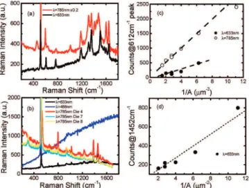
Figure 3a shows SERS spectra of R6G molecules (incubated at a concentration of 1× 10⁻⁶M) acquired at different
experi-mental conditions for die 4 characterized by Do) 180 nm and P ) 600 nm. The spectrum indicated by the red curve was taken at a Raman Micro Station R3 operating at the wavelength of λ ) 785 nm, whereas the black one represents the spectrum of the same die taken 6 weeks later at a LabRam HR instrument from Horiba Jobin Yvon operating at the wavelength of λ ) 633 nm. The spot size of the laser used for the Raman Micro Station R3 is 25 µm; the total number of the NWs sampled with its beam is about 2400, whereas in the measurements performed with LabRam HR, this number is less than four NWs. These two separate measurements demonstrate excellent stability of the fabricated SERS-active substrate.
Figure 3c shows an intensity plot of the 612 cm-1band which
is associated with the in-plane bending mode of the C-C-C ring as a function of 1/A for six dies containing identical NWs. We denote with A in this graph the square of the pitch such that 1/A stands for the number of NWs per unit area. This figure clearly shows that the output signal is directly proportional to the number of NWs per unit area regardless of the excitation wavelength and the instruments that were used for the measurements. This finding implies that the observed SERS effect is primarily a result of SERS enhancements from individual NWs. The slight scatter of the data is attributed to the small shifts of the SPR peaks in different dies (as shown in Figure 2).
The linear dependence of the SERS output signal on the number of NWs has also been confirmed by the detection of phthalazine molecules by the Laboratory Ram HR, as shown in Figure 3b. The intensity of the Raman peaks measured at λ ) 785 nm is stronger than that measured at λ ) 633 nm due to increase in laser power. However, there is no observable Raman peak from phthalazine when it is excited at λ ) 488 nm, although there is a broad plasmonic absorption peak near 500 nm. As
pointed out previously, this absorption peak comes from the continuous Au film base; it is associated with the propagating plasmons rather than the localized ones. Since the smooth Au film base does not contribute to the overall SERS signal, the measured SERS signal is solely a result of the patterned NW structure. The SERS spectra of phthalazine molecules at λ ) 785 nm for die 7 characterized by Do) 375 nm, P ) 500 nm and die 8 with Do) 492 nm, P ) 620 nm are also shown in Figure 3b. The total surface areas of the Au base film in dies 4, 7, and 8 are different. Assuming that the molecules are uniformly adsorbed on the Au surface, it is expected that the number of molecules attached on individual NWs increases from die 4 to die 7 and further on to die 8. After considering this effect, it is clear that the SERS enhancement factor of individual NWs is smaller for die 4 than for die 7, the enhancement in the latter being even smaller than that measured for die 8. This result indicates that the SERS enhancement factor is solely dependent on the geo-metrical parameters of individual NWs and it is completely independent of the Au base thin film.
We further validated the potential use of Au NWs as SERS platforms for the detection of nucleic acids using two relatively short (15 and 20 mer) single-stranded oligonucleotides as model systems. The first type of oligonucleotide was labeled with Cy3 fluorescent dye at its 5′position (sso1), whereas the other one was label-free (sso2). Both oligonucleotides entailed all four bases A, G, C, and T that were arranged in random order (see the Experimental Section for details). We relied on both physisorption of DNA molecules on bare Au NWs and covalent attachment of amino-modified oligomers involving a monolayer of 11-mercap-toundecanoic acid and activation of carboxylic acid groups with NHS/EDC.43Both methods allowed for recording SERS spectra
in a reliable manner. Typical SERS spectra of sso1 and sso2 on Au NWs (Do) 180 nm, Di) 50 nm, Au thickness is 35 nm, and
P ) 300 nm) are shown in Figure 4. The peak at 520 cm-1 is
attributed to the Si substrate again. For sso1, major peaks were observed at 560, 930, 1020, 1192, 1390, 1468, and 1588 cm-1, which
can be attributed to Cy3.44We do not observe signals from other
species including 11-mercaptoundecanoic acid and the bases of the nucleotide itself. In contrast, the spectrum obtained from sso2 comprised a mixture of Raman signals from individual bases:
(43) Johnsson, B.; Lo¨fa˚s, S.; Lindquist, G. Anal. Biochem. 1991, 198, 268. (44) Cao, Y. C.; Jin, R.; Mirkin, C. A. Science 2002, 297, 1536.
Figure 3.(a) SERS spectra of R6G molecules measured on Au NWs (die 4) at two excitation wavelengths. (b) SERS spectra of phthalazine molecules measured on Au NWs with different sizes (dies 4, 7, and 8) and different wavelengths of the incident laser beam. Plots of the counts at 612 cm-1for R6G molecules and 1452 cm-1for phthalazine
molecules as a function of the number of NWs per unit area 1/A are shown in (c) and (d), respectively.
Figure 4.SERS spectra of single-stranded DNA (ssDNA) conjugated with Cy3 (black curve) and label-free (red curve) recorded on Au NWs that correspond to die 1. The thickness of the Au film was 35 nm.
peaks at 650 and 1570 cm-1were attributed to G, 732 and 1320
cm-1to A, 1023 and 1635 cm-1 to C, whereas the peak at 790
cm-1corresponds to both C and T.45Although it was possible to
reconstruct the composition of the oligonucleotide in a qualitative manner, quantification of signal intensities still awaits further investigation. Plotting the counts at 1588 cm-1(Cy3) and those
at 790 cm-1 (C and T) as a function of 1/A retained a linear
relationship (data not shown), confirming potential suitability of Au NWs for analytical applications using SERS.
To gain a better insight into the field distribution around individual NWs, the local enhancement of the electromagnetic (EM) field was evaluated using a multiprocessor implementation of the discrete dipole approximation (DDA)46,47 with a lattice
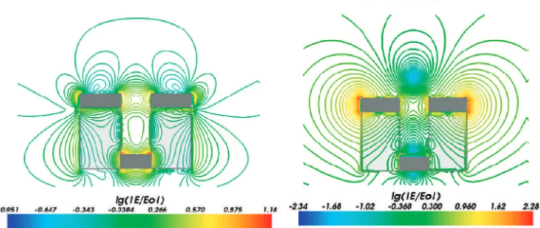
dispersion relation (LDR) prescription for individual polarizabilities at the nodes of the mesh. In our modeling, the NWs (as well as the surrounding free space) are meshed with a resolution of 3 nm, small enough to achieve high accuracy from the DDA algorithm. Figure 5 shows some scalar cross sections of the
near-field (left column) as well as isocurves of constant lg(E/E0) (right column) at a wavelength λ ) 785 nm for a single NW in dies 4 (Figure 5a), 7 (Figure 5b), and 8 (Figure 5c). As depicted in these figures, the hot spots are stronger and distributed over a larger surface area for the NW in die 4: on the nanodonut surface, the enhancement of the EM field E/E0reaches as much as 100 on both the top and lateral side. An enhancement of E/E0 was calculated to be more than 10 inside the whole cavity of the NW, as shown by the yellow region in Figure 5a. As observed from the contour line patterns, the bottom nanodisc undergoes dipolar electromagnetic oscillations, whereas the nanodonut on the top is obviously in a multipolar regime. Both nanodisc and nanodonut contribute to the enhancement of the electromagnetic field, the active regions of the nanodisc being located near its edge. However, near its median (central) region, the nanodisc presents a “dark spot” where the electromagnetic field is many times attenuated, and consequently it does not contribute to the SERS signal. As the size of the NW increases, the electromagnetic field enhancement becomes weaker and the hot-spot coverage shrinks. The enhancement factor lg(E/E0) drops from 2.7 (in die 4) to 2.4 or even 2.09 in dies 7 and 8, respectively. This decrease is accompanied by a reduction of the area of highly localized EM fields in the nanodonut at this wavelength. The important active
(45) Green, M.; Liu, F.-M.; Cohen, L.; Ko¨llensperger, P.; Cassc, T. Faraday
Discuss.2006, 132, 269.
(46) Yurkin, M. A.; Hoekstra, A. G. J. Quant. Spectrosc. Radiat. Transfer 2007,
106, 558.
(47) Yurkin, M. A.; Maltsev, V. P.; Hoekstra, A. G. J. Quant. Spectrosc. Radiat.
Transfer2007, 106, 546.
Figure 5.Scalar cut of the electromagnetic field enhancement (E/E0) in a plane defined by the NW symmetry axis and the polarization direction
of the incident light (left column) and isocurves of constant lg(E/E0) (right column) at λ ) 785 nm for a single NW whose geometrical parameters
correspond to dies 4 (a), 7 (b), and 8 (c). The gray regions stand for the optically active material (Au), the slightly shaded gray ones for the Si cylinder, whereas the rest is considered as free space (perfect vacuum).
region is located on the top surface of the nanodisc. At the edges of the nanodisc, the pattern of the resonance showed a multipolar contribution from the electric oscillations. All these simulation results are in good agreement with the SERS experimental results shown in Figure 3b.
The near-field distribution and the field enhancement lg(E/
E0) have also been computed at different wavelengths, namely, λ ) 500 and 1050 nm for the Au NWs in die 4. As shown in Figure 6, at short wavelengths, the charge distribution in the nanodonut corresponds to opposite signs for the inner and outer surfaces of the wall, which are two pairs of dipolar charge distributions. However, the field enhancement E/E0 decreases dramatically when compared to that at λ ) 785 nm. Although there are some regions of high field contributions located near the nanodisc, the field enhancement becomes generally weaker in this case. This is in good agreement with the SERS experimental results at λ ) 488 nm wavelength. At wavelengths in the NIR range, the charge distribution in nanodonuts has the same sign for the inner and outer surface of the wall, the whole NW being equivalent to a big electric dipole. These strong dipolar excitations involve the entire nanodonut perimeter and result in large field enhancements in the NIR regime, even though the nanodisc is almost “extin-guished” at these wavelengths.
CONCLUSIONS
We introduced Au NWs as stable and efficient nanostructures with two tunable plasmon resonances, one being located in the visible and the other in the NIR regime. SERS spectra of both
R6G and phthalazine molecules adsorbed on the Au NWs confirmed that the NWs are SERS active over a wide range of wavelengths. These nanostructures further proved useful as SERS platforms in analytical applications including the detection of DNA in both labeled and label-free forms. Numerical calculations indicate that SERS enhancements are attributed to hot spots located both inside and outside individual NWs. On the other hand, far-field intercoupling effects between NWs have been observed in arrays with pitch in the subwavelength regime. In principle, the double-SP resonances present in these Au nano-structures as well as the tunable SERS activity suggest that they should provide increased selectivity in the detection of molecules by accurately tailoring the geometric parameters of the NWs for either SPR or SERS applications.
ACKNOWLEDGMENT
This work was supported jointly by the National Research Council’s Genomics and Health Initiative Program and the Industrial Materials Institute. We thank the Re´seau que´be´cois de calcul de haute performance (RQCHP) for providing the compu-tational resources. We are gratefully thankful for the assistance of Joanne Zwinkels, Nelson Rowell and John Hulse for making the UV-Vis spectrometer available for our use.
Received for review January 21, 2008. Accepted April 7, 2008.
AC800149D
Figure 6.Isocurves of constant lg(E/E0) of the electromagnetic field at λ ) 500 and 1050 nm for individual NWs corresponding to die 4.