Publisher’s version / Version de l'éditeur:
Applied Physics Letters, 95, 18, pp. 183505-1-183505-3, 2009-11-05
READ THESE TERMS AND CONDITIONS CAREFULLY BEFORE USING THIS WEBSITE. https://nrc-publications.canada.ca/eng/copyright
Vous avez des questions? Nous pouvons vous aider. Pour communiquer directement avec un auteur, consultez la
première page de la revue dans laquelle son article a été publié afin de trouver ses coordonnées. Si vous n’arrivez pas à les repérer, communiquez avec nous à [email protected].
Questions? Contact the NRC Publications Archive team at
[email protected]. If you wish to email the authors directly, please see the first page of the publication for their contact information.
NRC Publications Archive
Archives des publications du CNRC
This publication could be one of several versions: author’s original, accepted manuscript or the publisher’s version. / La version de cette publication peut être l’une des suivantes : la version prépublication de l’auteur, la version acceptée du manuscrit ou la version de l’éditeur.
For the publisher’s version, please access the DOI link below./ Pour consulter la version de l’éditeur, utilisez le lien DOI ci-dessous.
https://doi.org/10.1063/1.3257729
Access and use of this website and the material on it are subject to the Terms and Conditions set forth at
Highly efficient cross-linked PbS nanocrystal/C60 hybrid heterojunction
photovoltaic cells
Tsang, S. W.; Fu, H.; Wang, R.; Lu, J.; Yu, K.; Tao, Y.
https://publications-cnrc.canada.ca/fra/droits
L’accès à ce site Web et l’utilisation de son contenu sont assujettis aux conditions présentées dans le site LISEZ CES CONDITIONS ATTENTIVEMENT AVANT D’UTILISER CE SITE WEB.
NRC Publications Record / Notice d'Archives des publications de CNRC: https://nrc-publications.canada.ca/eng/view/object/?id=7ad96b8f-48c3-4235-9e08-4efabf2fb11e https://publications-cnrc.canada.ca/fra/voir/objet/?id=7ad96b8f-48c3-4235-9e08-4efabf2fb11e
Highly Efficient Cross-linked PbS Nanocrystal/C60 Hybrid Heterojunction Photovoltaic
Cells
S. W. Tsang,1 H. Fu,1 R. Wang,2 J. Lu,1 K. Yu,2 and Y. Tao1,a
1
Institute for Microstructural Sciences, 2Steacie Institute for Molecular Sciences, National
Research Council of Canada, Ottawa, Ontario, Canada K1A 0R6
Abstract
We present a highly efficient hybrid heterojunction photovoltaic (PV) cell with a colloidal inorganic nanocrystal (NC) electron donor and an organic electron acceptor. The heterojunction is formed by a thin film of cross-linked PbS NCs and a vacuum deposited C60 layer. Compared to
the PbS-only PV cell, the heterojunction device has improved the power conversion efficient (PCE) from 1.6 % to 2.2 % under one sun of simulated Air Mass 1.5 Global (AM 1.5G) irradiation. The C60 layer effectively prevents exciton quenching at the NC/metal interface, as
evidenced by a significant improvement in fill-factor (FF) of the heterojunction devices. In addition, a slightly larger open-circuit voltage (VOC) obtained in the heterojunction devices also
suggests that there is an efficient charge transfer between PbS NCs and C60 through the NC
surface linkers to generate a depletion region. This is further supported by the photoluminescence (PL) quenching experiment of the hybrid system.
Solution processable thin film photovoltaic (PV) devices based on organic electron donor and acceptor materials have recently achieved over 6 % power conversion efficiency (PCE).1
Owing to the large energy bandgap (> 1.8 eV) of those organic materials, only the visible region in the solar spectrum can be harvested, leaving ~50 % of the solar irradiance abandoned. Colloidal semiconductor nanocrystals (NCs) are believed as an alternative or a complementary material that is compatible with the low-cost solution processes for PV application. By controlling the size of the NCs during the synthesis, light absorption can be tuned in a wide spectral range from infrared (IR) to visible. PbS NC is one of the prototypical materials used in PV application. Schottky-type PV cells based on PbS NCs have been reported with a PCE of 1.7-1.8%. 2,3 It has also been demonstrated that a Schottky-type PV cell fabricated with a single layer
of ternary PbSXSe1-X NCs can achieve a PCE as high as 3.3 %. 3
However, the maximum open-circuit voltage (VOC) of such a Schottky-type PV cell is limited to the half of the energy bandgap
(Eg) of the NC.4 Moreover, surface recombination centers as commonly present in the semiconductor/metal interfaces also lower the quantum yield of the device. Therefore, it is believed that a p-n or a p-i-n type heterojunction structure can overcome the limitations and enhance the device efficiency by increasing the VOC and shifting the exciton dissociation region
away from the metal electrode. However, a few major criteria have to be met for an efficient heterojunction device: the combination of the energy levels of the donor and acceptor materials should provide a considerable built-in potential to dissociate the photo-generated excitons; the electron coupling between the donor and acceptor materials should be strong enough to facilitate exciton dissociation and charge transport at the heterojunction. In addition, since the surface ligands play a key role in determining the interaction between the donor and acceptor materials in the heterojunction device, and thus affect directly the electronic properties of the heterojunction devices, the long chain insulating surface ligands that are commonly used to cap the colloidal NCs during synthesis must be removed or replaced in order to make the NCs electronically active. In the recent work on PbS/C60 hybrid heterojunction devices, Dissanayake et al have significantly
improve the short-circuit current density (JSC) of their devices, however the VOC is largely
reduced.5 The PCE of their hybrid heterojunction PV cell is lower than 0.5 %. Since the NC thin
film was treated in methanol in their case to remove the surface ligands, the process of which might lead to the increase of surface trap density and thus alter the energy alignment at the heterojunction.
In this work, we demonstrate a highly efficient hybrid heterojunction PV cell with cross-linked PbS NCs and a C60 layer. The heterojunction cell has a significant improvement in PCE.
The achieved efficiency in the heterojunction cell is the highest among those similar material systems and the PbS NC only PV cells reported in the literature. Detailed discussions are given on the electrical and optical characterizations of the heterojunction devices.
Colloidal PbS nanocrystals were synthesized according to the methods reported by Hines
et al 6 and Liu et al 7 with modifications. The synthesized PbS NCs were ~4 nm diameter and capped with oleic acid (OA) as the surface ligand. The first excitonic transition λex1 of the NCs
was at 1220 nm. The NCs were purified by using a combination of solvent/nonsolvent pairs (toluene/methanol first, hexanes/acetone second). For the PV cell fabrication, indium-tin-oxide (ITO) coated glass was used as the anode. Immediately prior to device fabrication, the ITO glass was cleaned by ultra-sonic baths of organic solvents and UV-ozone treatment for 15 min. A 5 mg/mL solution of PbS-OA in chloroform was used to prepare the active layer. The cross-linked PbS NC thin films were fabricated with the layer-by-layer method reported by Nozik et al.8
1,3-benezendithiol (BDT) was used as the cross-linker to replace the OA surface ligand and bridge the NCs. Instead of using dip-coating, we employed successive spin-casting to prepare the NC layers. Each step produced a 7 ~ 8 nm of PbS-OA film corresponding to 1-2 monolayers of the NCs, and then the film was soaked into a 0.02 M BDT solution in acetonitrile for cross-linking. For the hybrid PV cell, a C60 layer was thermally evaporated on top of the NC at a base pressure
had a general structure of ITO / PbS-BDT (90nm) / C60 (x nm) / LiF (1 nm) / Al (120 nm) with an
active area of 6.9 mm2.
The PV cells were characterized in air under one sun of simulated Air Mass 1.5 Global (AM 1.5G) solar irradiation (100 mWcm-2, Sciencetech Inc., SF150). The light intensity was
calibrated with a power meter (Gentec Inc., UP19K-30H-H5). The current density-voltage (J-V) characteristics were measured with a Keithley 2400 source meter. For the photoluminescence (PL) measurements, the PbS-OA and PbS-BDT films with the same thickness (90 nm) were prepared on quartz substrates and excited with a monochromatic source at 950 nm. The film thicknesses were measured by a Dektak profilometer.
Fig. 1 shows the J-V characteristics of the PbS-BDT only and the hybrid heterojunction PbS-BDT/C60 PV cells. With the addition of a 30 nm C60 layer, the overall performance of the PV
cell is improved. The JSC is increased from 9.9 mA/cm2 to 10.5 mA/cm2, the VOC is slightly
increased from 0.39 V to 0.40 V, and the fill-factor (FF) is significantly increased from 40% to 52%. This leads to the increase of the PCE from 1.6 % to 2.2 %. For the PbS-BDT only PV cell, the photo-generated excitons dissociate in the depletion layer formed beside the PbS-BDT/Al interface. However, it is well known that surface recombination centers are always present at the semiconductor/metal interfaces. The excitons would readily quench at such an interface without dissociation into free carriers. For the heterojunction cell, the increase in VOC and FF suggests a
reduced recombination current in the device. Excitons dissociate more efficiently at the PbS-BDT/C60 interface. Furthermore, as compared to the Schottky-type PbS-BDT only PV cell, the
larger VOC in the heterojunction cell suggests that the depletion layer is also formed in the
PbS-BDT layer. As both ITO/PbS and C60/LiF/Al contacts are Ohmic,9 charges can readily diffuse to
the donor and acceptor materials. An efficient charge transfer at the heterojunction can facilitate the formation of depletion at the heterojunction.
The improvement in efficiency of the heterojunction cell is also supported by the external quantum efficiency (EQE) measurement results as shown in Fig. 2 (a). Compared to the PbS-BDT only device, the heterojunction cell has a higher EQE over a broad spectral range. The EQE of the heterojunction cell is over 40 % from 380 nm to 570 nm. According to the EQE data, the
JSC under 100 mW/cm2 of AM 1.5G solar irradiation is calculated to be 10.2 mA/cm2. This is
consistent with the JSC measured from the J - V results, demonstrating negligible spectral
mismatch in the PCE measurement. The improvement in EQE is attributed both to the enhanced optical absorption in the device, and to the more efficient excitons dissociation at the PbS-BDT/C60 interface. The increased EQE in the spectral range between 400 nm and 600 nm is
possibly contributed by the optical absorption of the C60 layer, and also the induced optical cavity
effect in the devices as shown in the measured 1-Reflectance plot in Fig. 3. By assuming negligible internal reflection inside the device, the lower limit of the internal quantum efficiency (IQE) can be estimated with the measured specular reflectance from the device, i.e. IQElower limit =
EQE / (1 – Reflectance). As shown in Fig. 2 (b), the IQElower limit of the heterojunction cell has
increased in the spectral range above 500 nm by over 10% while it remains nearly unchanged in the short wavelength region. This may be due to the fact that although the first excitonic transition λex1 of the NCs is at 1220 nm, the optical absorption in the visible region is much
stronger than that in the near infrared (NIR) region. Therefore, higher energy photons in the visible region are strongly absorbed by the PbS-BDT film close to the anode side, and the lower energy photons can penetrate deeper into the cathode side of the device. By considering the AM 1.5G photon flux and the measured absorbance of PbS-BDT thin film, the number of photons in the NIR region reaching the cathode side is around three times more than those photons with wavelength below 500 nm. Since C60 has no absorption in the NIR region, the improved IQElower
limit of the heterojunction device in this region proves that the exiton dissociation is more efficient
at the PbS-BDT/C60 than the PbS-BDT/Al interfaces. It is also demonstrated with the improved
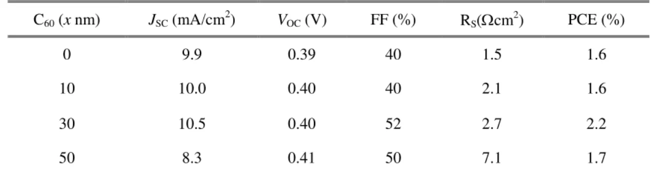
The performance of the heterojunction PV cells with C60 layer of different thicknesses is
summarized in TABLE 1. Generally, the heterojunction PV cells have higher VOC. The FF is
increased by 10 % with 30 nm and 50 nm C60. The maximum PCE is obtained with 30 nm C60.
For the device with 50 nm C60, although it is optically favorable as shown in Fig. 3, the JSC is
significantly reduced as the device has a larger series resistance RS. Previously reported
PbS/C60 heterojunction devices have higher JSC but a lower VOC than those of the PbS-only
devices where the PbS NC thin film was treated with methanol for removing the surface ligand to increase the conductivity.5 Although most of the as synthesized NCs are capped with insulating
ligands, it is essential to passivate the reactive NC surface. The lower VOC may be due to the
presence of surface traps which alters the energy level alignment at the PbS/C60 interface. For the
BDT capped PbS NCs as presented in this study, the VOC is increased in the heterojunction
devices. As the VOC is mainly determined by the build-in potential established in the depletion
region of the PbS NC layer, the increase suggests efficient charge transfer between the PbS and C60 through the BDT surface ligands. This is further supported by the PL measurement results of
the single and bilayer thin films as shown in Fig. 4. The PL quenching experiment has been widely used to characterize the ultrafast charge transfer in NC and organic materials.10,11 The
PbS-OA NC thin film shows a much stronger PL signal. The long chain OA (l = 2 nm) surface ligands effectively isolate the NCs from each other. However, after the ligands are replaced with BDT (l = 0.3 nm), the PL signal is significantly reduced by more than one order of magnitude. Moreover, the peak position is red-shifted by 50 nm. Consequently, the short BDT surface ligands increase the electron coupling between the NCs and other electronic materials. For the bilayer PbS-BDT/C60 film, the PL signal is completely quenched. Since C60 has negligible
absorption in the NIR region, charge transfer instead of energy transfer should be the most possible mechanism for the observed PL quenching. This confirms that the BDT surface ligands not only passivate the PbS NCs surface, but also facilitate the charge transfer in PbS NCs and C60
In conclusion, we have demonstrated a highly efficient PbS NC / C60 hybrid
heterojunction photovoltaic cell. The PCE is increased from 1.6 % in the NC only device to 2.2 % in the heterojunction device under AM 1.5G irradiation. Besides the reduced exciton quenching in the heterojunction device, the BDT surface ligand provides an efficient pathway to facilitate charge transfer between the NC and C60, which is supported by the higher VOC obtained in the
heterojunction device and the PL quenching experiment. The results presented here provide an insight into the future development of PV heterojunction devices with NCs and organics.
Acknowledge
The authors would like to acknowledge the financial support from the National Research Council of Canada’s NRC-Nano program. H.-Y. Fu thanks the Chinese Scholarship Council for providing her PDF scholarship.
References
1 S. H. Park, A. Roy, S. Beaupre, S. Cho, N. Coates, J. S. Moon, D. Moses, M. Leclerc, K. Lee, and A. J. Heeger, Nat. Photon. 3, 297 (2009).
2 W. J. Keith, G. P. A. Andras, P. C. Jason, H. M. Stefan, D. M. Dean, L. Larissa, and H. S. Edward, Appl. Phys. Let. 92, 151115 (2008).
3 W. Ma, J. M. Luther, H. Zheng, Y. Wu, and A. P. Alivisatos, Nano Letters 9, 1699 (2009).
4 J. Nelson, The Physics of Solar cells (Imperial College Press, London, 2003).
5 D. M. N. M. Dissanayake, T. Lutz, R. J. Curry, and S. R. P. Silva, Nanotechnology 20, 245202 (2009).
6 M. A. Hines and G. D. Scholes, Adv. Mater. 15, 1844 (2003).
7 T. Y. Liu, M. Li, J. Ouyang, M. B. Zaman, R. Wang, X. Wu, C. S. Yeh, Q. Lin, B. Yang, and K. Yu, J. of Phy. Chem. C 113, 2301 (2009).
8 J. M. Luther, M. Law, M. C. Beard, Q. Song, M. O. Reese, R. J. Ellingson, and A. J. Nozik, Nano Letters 8, 3488 (2008).
9 X. D. Feng, C. J. Huang, V. Lui, R. S. Khangura, and Z. H. Lu, Appl. Phys. Lett. 86, 143511 (2005).
10 N. C. Greenham, X. Peng, and A. P. Alivisatos, Phys. Rev. B 54, 17628 (1996). 11 D. S. Ginger and N. C. Greenham, Phys. Rev. B 59, 10622 (1999).
Table I Summary of the performance of the ITO/PbS-BDT (90 nm)/ C60 (x nm) / LiF/Al PV cells. C60 (x nm) JSC (mA/cm 2 ) VOC (V) FF (%) RS(Ωcm 2 ) PCE (%) 0 9.9 0.39 40 1.5 1.6 10 10.0 0.40 40 2.1 1.6 30 10.5 0.40 52 2.7 2.2 50 8.3 0.41 50 7.1 1.7
Figure captions
Figure 1
Current density-voltage (J-V) characteristics of the PV cells with (solid line) and without (dashed line) a 30 nm C60 layer. The black curves represent the dark current and the red curves represent
the devices under 100 mW/cm2 of simulated AM 1.5G irradiation.
Figure 2
(a) Measured external quantum efficiency (EQE) of the PV cells with (solid line) and without (dashed line) an additional 30 nm C60 layer. (b) Estimated lower limit of the internal quantum
efficiency (IQElower limit) of the PV cells using the EQE and 1-Reflectance results as shown in Fig.
2(a) and (3) respectively.
Figure 3
Measured 1-Reflectance plot of the PV cells, ITO / PbS-BDT (90 nm) / C60 (x nm) / LiF / Al,
with an additional C60 layer of different thicknesses.
Figure 4
PL intensities of PbS-OA (black), PbS-BDT (red), and PbS-BDT / C60 (blue) thin films on quartz
Figures