Preprint typeset in JINST style - HYPER VERSION
CALICE Report to the DESY Physics Research Committee
The CALICE Collaboration
∗ABSTRACT: We present an overview of the CALICE activities on calorimeter development for a future linear collider. We report on test beam analysis results, the status of prototype development and future plans.
∗The complete list of current CALICE authors can be found in Appendix 1.
Contents
1. Introduction 3
2. Silicon-Tungsten ECAL: SiW 4
2.1 Introduction 4 2.2 Physics prototype 4 2.3 Technological prototype 5 2.3.1 Sensors 5 2.3.2 ASIC 6 2.3.3 PCB 6 2.3.4 Integration 8
2.3.5 Data acquisition system 8
2.3.6 Mechanical structure 9
2.3.7 Cooling 10
2.4 Future Plans 10
3. Scintillator Strip ECAL: ScECAL 10
3.1 Operational experience with physics prototype 10
3.2 Next generation engineering prototype and current status 11
3.2.1 Strip clustering algorithm development 11
3.2.2 Layer electronics development 12
3.2.3 5 mm scintillator development 13
3.2.4 MPPC development 13
3.3 Future R&D 14
4. Digital ECAL: DECAL 14
4.1 Context 14
4.2 Testbeams in 2010 14
4.3 Pixel efficiency results 15
4.4 Future plans 15
5. Analogue HCAL Technological Prototype 16
5.1 Tiles and ASICs 16
5.2 Detector/DAQ interface 17
5.3 Light calibration system 18
5.4 Measurements and results 19
5.5 Future plans 20
6. Tungsten Analogue HCAL: W-AHCAL 20
6.1 Motivation 20
6.2 Experimental prototype 20
6.3 T3B: Time Structure of Hadronic Showers in the W-AHCAL 23
7. Digital HCAL: DHCAL 24
7.1 RPC-based DHCAL 24
7.1.1 Description of the project 24
7.1.2 Past achievements since the last review 25
7.1.3 First DHCAL results 27
7.1.4 Future plans 27
7.2 GEM-based DHCAL 28
7.2.1 GEM 30 cm × 30 cm prototype tests with KPiX readout system 28
7.2.2 Pressure dependence corrections 31
7.2.3 Evolution to large area chamber 32
7.2.4 Progress on thick-GEM alternative approach 32
7.2.5 DCAL digital readout integration 33
7.2.6 Future plans 33
8. Semi-digital HCAL: SDHCAL 33
8.1 RPC-based SDHCAL 34
8.1.1 Detector design 34
8.1.2 Electronic readout 35
8.1.3 Data acquisition 35
8.1.4 Cassette 36
8.1.5 Tests and results 36
8.1.6 Mechanical structure 38
8.1.7 Prototype construction 38
8.2 MICROMEGAS-based SDHCAL 38
8.2.1 Small prototypes 38
8.2.2 Active sensor units of 48×32 cm2 39
8.2.3 First prototype of 1 m2 39
8.2.4 Beam test 39
8.2.5 ASIC development 39
8.2.6 Future plans 40
9. Front-End Electronics 41
9.1 DHCAL technological prototype 41
9.1.1 HARDROC ASIC 41
9.1.2 MICROROC ASIC 43
9.2 AHCAL technological prototype 44
9.3 ECAL technical prototype 46
9.4 Conclusion 47
10. Data Acquisition 47
10.1 Functional specifications 47
10.2 Implementation 49
10.3 Planning & organisation 50
10.4 Hardware availability 50
10.5 Firmware & implemented functionalities 51
10.6 Software 51
11. Test Beam Analysis Results 52
11.1 Si-W ECAL performance 52
11.2 AHCAL performance 53
11.3 Combined calorimeter system 54
11.4 Sc-W ECAL performance 55
11.5 DHCAL performance 55
11.6 WHCAL and T3B results 57
11.7 Effects of high-energy particle showers on the embedded front-end electronics 59
12. Future Beam Test Plans 60
12.1 Physics prototypes 60
12.2 Technical prototypes 61
12.3 Concluding remarks on test beams 62
13. Summary and Outlook 62
14. Acknowledgments 64
1. Introduction
The CALICE Collaboration pursues the development of highly granular calorimeters for a future e+e− linear col-lider, based on the particle flow approach for optimal overall detector performance. The Collaboration consists of 57 institutes from 17 countries in Africa, America, Asia and Europe and has about 350 physicists and engineers as members.
We are investigating several technological options for both electromagnetic and hadronic calorimeters. Most of these are candidates for both of the particle flow based ILC detector concepts, ILD and SiD, and for a detector at a multi-TeV linear collider such as CLIC. Our aim is to cover the widest possible range of options with prototypes and to test them using particle beams, thereby maximizing the use of common infrastructure such as mechanical devices, ASIC architecture or DAQ systems. Wherever it is technically feasible and expedient, we work within a common software and analysis framework. This facilitates combination and comparison of test beam data while reducing systematic effects, and allows us to achieve a common understanding of the relative strengths and weaknesses of the options under consideration. This is one of the main strengths of a broadly-based collaboration such as CALICE.
The major part of the effort is focused towards presenting realistic proposals for the detector concept reports of the ILC Technological Design Phase 1, which is due in 2012. This is closely co-ordinated with the detector concept groups. Given the as yet uncertain schedule and energy range that will be required of the future lepton collider, we are also pursuing developments which will only reach a similar level of maturity at a later stage.
The development of calorimeter prototypes generally proceeds in two steps. Physics prototypes provide a proof-of-principle of the viability of a given technology in terms of construction, operation and performance. In addition they are used to collect large data sets for the study of hadronic shower evolution with high granularity. These are invaluable for testing shower simulation programs, and for the development of particle flow reconstruction algorithms with real data.
In contrast, technological prototypes address the issues of scaling, integration and cost optimization. Due to the differing responses of the various active media used to the components of hadronic showers, the physics prototypes are necessary for each combination of active and passive materials under consideration. Technical prototypes are required for each technology, but the effort can be kept to an acceptable level by using common building blocks, and by addressing large area and multi-layer issues separately without instrumenting a full volume.
Synopsis
The completion of data taking with physics prototypes of a silicon based ECAL and scintillator based ECAL and HCAL was reported in 2009. Since then, emphasis has shifted towards analysis of these data, as illustraed by the new results reported here, including detailed comparisons with Geant4- based simulations and a first test of state-of-the art particle flow reconstruction with combined ECAL and HCAL test beam data.
In the meantime, construction of the first gaseous digital HCAL prototype was finished, with front end electronics already integrated in the detector volume. Data taking started in 2010 at the Fermilab test beam facility, using the existing absorber structure and stage. We present first results on detector performance and the status of data taking, which is ongoing in conjunction with the silicon ECAL at the time of this review.
The year 2010 also saw the start o beam tests for a new tungsten HCAL absorber structure, as proposed for the CLIC energy range. Here, the well-understood active scintillator layers are being re-used. We report on a first look into the time structure of the hadronic response in a neutron-rich material.
Major progress was also made with technological prototypes with highly integrated ultra-low power electronics. Final versions of mixed-circuit read-out ASICs were mass-produced and successfully tested, including power-pulsed operation in high magnetic fields. The full read-out chain of the second generation scalable DAQ was established.
The biggest effort here is the construction of an RPC based semi-digital cubic metre scale HCAL prototype for beam tests in 2011, which will establish the electronics integration concept at large scale and contribute to the study of hadronic interactions seen with highly granular gaseous read-out.
Smaller scale technical tests, some ranging up to square-metre sized active layers, were carried out with all con-sidered HCAL read-out technologies, with GEMs, micromegas and scintillator, and are being prepared for the ECAL.
2. Silicon-Tungsten ECAL: SiW 2.1 Introduction
A high granularity ECAL is a central component of a particle-flow optimized detector. It should efficiently identify photons and measure their energy with reasonable precision, and should have excellent capabilities (in conjunction with other subdetectors) to distinguish photonic depositions from those due to other particle types. A sampling calorimeter naturally gives the required granularity in one dimension, while a highly segmented design of the readout layers provides it in the other two dimensions. The choice of tungsten as an absorber material is motivated by its small Molière radius and radiation length and the large difference between its radiation and interaction lengths, ensuring that photonic showers are of small size, and with a significantly different size to hadronic showers. The use of matrices of PIN diodes in high resistivity silicon allows an efficient and low-noise detection of charged particles, and the possibility to efficiently implement highly segmented readout.
2.2 Physics prototype
A first detector prototype, known as the “physics prototype” was constructed during the years 2005–2007. It had an active area of 18 × 18 cm2 and 30 sampling layers. It was extensively tested in particle beams between 2006 and
2008 at CERN and FNAL (as seen in Fig.1). These tests were performed as part of the combined CALICE test beam
campaigns with the ECAL followed by a (scintillator-based analogue readout) hadronic calorimeter, and a tail-catcher system, and used beams of electrons, muons and pions with energies between 2 and 180 GeV.
In 2011, the physics prototype will again be placed into test beams at FNAL, this time with a RPC-based digital readout hadronic calorimeter, allowing detailed comparisons between the two HCAL approaches.
The measured performance of this prototype has demonstrated that the silicon tungsten approach can satisfy the various requirements for detector performance at a future lepton collider. The detector has run stably over a period of five years without showing any signs of aging.
Figure 1. Physics prototype installed at a test beam.
2.3 Technological prototype
The focus is now is on the development of the technologies necessary for such a calorimeter to be integrated into a full detector, keeping in mind that large scale, industrialised construction and quality control will be necessary when a final detector is built. Factors considered include a modular design using low power front end electronics integrated into the detector volume, realistic mechanical supporting structures, a compact leak-less cooling system.
The general design of the module is shown in Fig.2; details can be found in [1]. The composite-tungsten mechan-ical structure is a slightly scaled down version of a barrel module envisaged for a linear collider detector, with a length of 1.5 m and a width of around 55 cm, and a total weight of around 600 kg. It has a trapezoidal shape and consists of 15 × 3 alveola into which sensitive detector slabs are inserted.
Each detector slab is built around a “H” structure with a tungsten core and composite walls. Both sides of this structure are equipped with active elements consisting of the silicon sensors, a PCB which routes signals and commands between the interior and exterior of the detector, and the front end ASICs embedded into the PCB thickness. A Kapton cable provides the high voltage to the sensors, and a sheet of copper helps to extract the heat to a dedicated heat exchanger at the end of the module. A small Detector InterFace board at the end of each slab is the first element of the common CALICE DAQ system, as described in more detail in Sect. 10
For the technical prototype, a tower with an area of 18 × 18 cm2will be instrumented in all 30 layers, and one long detector slab will be built to test the propagation of signals over long distances within the calorimeter.
2.3.1 Sensors
The silicon sensors used in the ECAL are arrays of 5 × 5 mm2PIN diodes made in 300–500µm thick high resistivity silicon, and reverse biased at around 200 V. The sensors envisaged for the technical prototype have a total area of 9 × 9 cm2. A guard ring structure at the edge of the sensor protects against breakdown. A photograph of such a sensor is shown in Fig. 3.
Current studies include the minimisation of the guard ring region (an effectively dead detector region), and the understanding of the cost drivers for mass production (in close collaboration with industrial partners), with a view to reducing the eventual cost.
Around 40 sensors have already been purchased from HPK, further sensors will have different characteristics: relaxed quality control tolerances (a few dead or noisy channels do not pose a serious problem in reconstruction), more aggressive laser cutting of the wafer to minimise the edge area, and sensors sourced from other manufacturers.
Figure 2. Design of the technological prototype. The left figure shows an overview of the mechanical structure and the instrumented region, while the right figure shows a section of a detector slab.
Figure 3. A photograph of a 9 × 9 cm2silicon sensor from Hamamatsu Photonics with 5.5 mm pixels. The inset shows a microscopic view of the guard ring area: the length of the red arrow corresponds to 750 µm.
2.3.2 ASIC
A dedicated front end ASIC with 64 channels (SKIROC2) will be used to read the signals from the PIN diodes. It is designed to give a wide dynamic range (from 0.5 to 2500 MIP signals in the sensor), low signal to noise at the single MIP level (around 17 at 1 MIP), and low power consumption, at the level of 25 µW/channel (using the power pulsing technique). The schematic of the ASIC is shown in Fig.4. More than 1000 such chips have been produced, and are in the process of being tested.
2.3.3 PCB
The sensitive layers of the ECAL will be made up of several identical modules, known as Active Sensor Units (ASUs). An ASU is based around a large and thin 8-layer PCB (thickness of around 1 mm, area of 18 × 18 cm2) which hosts
Figure 4. Schematic of the SKIROC2 ASIC.
Figure 5. View of the PCB with integrated front end ASIC.
16 SKIROC2 ASICs on one side, and on the other side of which are glued the silicon sensors. Signals (both for configuration and data) are routed along lines in the intermediate layers.
Several prototypes of the PCB have been produced, for both packaged and unpackaged ASICs. The main obstacle at present is the planarity of the PCB, particularly for thin models: since rather delicate silicon sensors will be glued to the card, it should not be quite flat. Present prototypes have deviations of several millimetres from perfect planarity over the full area of the card. Modified assembly procedures (temperature/time allowed for cooling) and/or design may result in a flatter PCB, and are under test.
In the case of unpackaged ASICs (as envisaged for the final prototype), the ASICs will be contained within the volume of the PCB, and wire bonded to pads on the PCB. A test of this procedure (results shown in Fig.5) has already been carried out at the CERN bonding lab. Tests of an epoxy protection layer for the ASICs and wire bonds are underway.
The bias voltage (200 V) will be supplied to the sensors via a flat Kapton cable, prototypes of which have been successfully produced and tested, and a ∼ 500 µm thick copper layer is used to extract the heat at the end of the slab.
Figure 6. View of a “thermal slab”, used to test integration techniques and to measure the thermal properties of the mechanical structure. Visible is a chain of interconnected test ASUs, and the continuous copper sheet which acts as a heat drain.
Figure 7. DAQ test hardware: prototype ASU - adapter board - Detector InterFace card.
2.3.4 Integration
The task of assembling several ASUs into a detector slab is also under study. The connection between ASUs must be both mechanical and electrical (since signals are routed along the entire length of a detector slab). A previously developed technique involved the deposition of solder paste using a silk-screen and brief heating under a halogen lamp. This technique works well, but is rather labour intensive and requires great care: somewhat impractical for the future industrialisation of the process. A simpler process, based on the use of anisotropic conductive film (ACF), seems to be a very promising alternative. Tests have already been carried out in conjunction with the 3M company, with good results. The main question is whether the fully equipped ASUs can withstand the pressure required to bond the ACF without the fracture of the silicon sensors.
A dedicated assembly laboratory is being prepared at LAL, which will have all necessary equipment to assemble the slabs in a suitable and dedicated environment. A large-scale test of the integration procedure has already been performed for the assembly of the “thermal slabs”, as shown in Fig.6.
2.3.5 Data acquisition system
The common CALICE data acquisition system is described in Sect. 10. The integration of the system is continuing, with recent progress including the configuring of the ECAL ASICs via the complete DAQ chain. The various pieces of hardware of the system have been produced, and good progress has been made of the development of the necessary firmware and software. Fig. 7 shows some of the hardware used to test the DAQ chain, with a prototype ECAL ASU (left), an adapter board (centre), and the Detector InterFace card on the right. The full system will be tested using cosmics and particle beams during 2011.
Figure 8. View of the composite-tungsten demonstrator structure used to validate the construction technique.
Figure 9. Parts of the final mechanical structure awaiting the final assembly step.
2.3.6 Mechanical structure
The mechanical supporting structure developed for the technical prototype is close in shape and size to a barrel module envisaged for the barrel part of a linear collider detector (e.g. ILD). It is based on an alveolar structure made in carbon fibre composite material, and incorporates half of the tungsten absorber plates. This allows a modular structure suitable for industrialisation, and minimises the non-instrumented detector regions.
A small “demonstrator” structure, shown in Fig.8, has already been built to validate the assembly methods and materials. It was produced within the required tolerances.
The pieces for the final structure have been produced (as seen in Fig. 9), and an assembly mould has been designed and constructed. Studies to better understand the final thermal curing of the composite are underway in order to ensure successful assembly (there is no possibility to re-do the final curing, so care must be taken!).
The manufacture of the “H” structures is at present on hold, waiting for a definite answer on the feasibility of a sufficiently thin and flat PCB.
The production of longer alveolar structures, required for the endcap detectors (up to 2.5 m long in the current design of ILD) are also under study. The additional length requires extra care to be taken in the manufacture to ensure that the various pieces of the mould can be successfully extracted after the curing of the composite material.
Figure 10. Cooling tests using the demonstrator module. The ends of the nine thermal slabs are visible at the end of the mechanical structure, as is the copper heat exchanger connected to the slabs’ thermal drain.
2.3.7 Cooling
The “demonstrator module” has been used to understand the thermal properties of the composite/tungsten alveolar structure. A number of thermal detector slabs have been produced which produce heat at a number of points in a controllable manner, and also measure the temperature. A cooling system has been developed based on cold water circulation. It has been tested and has sufficient performance (with a reasonably generous margin) to cope with the expected power dissipation of the ECAL. This results of the thermal tests have been used to tune thermal simulations of the module’s behaviour, and to apply the same model parameters to simulation of the full technical prototype module and also the entire ECAL system within the ILD detector.
2.4 Future Plans
A first, partially equipped ASU readout using the full CALICE DAQ system will be tested in cosmics and beams during 2011. This will be equipped with a previous version of the ASIC (SPIROC2). Once we are confident that a sufficiently thin and flat PCB can be produced, the “H” structures can be produced. In the case that they cannot, we may proceed with a temporary solution in the short term: a “U” structure holding a single sensitive layer per alveola, which considerably relaxes the constraint on the PCB thickness.
The structure will be gradually equipped, testing various different approaches to the various technical challenges in order to understand their respective strong and weak points.
Once a reasonable number of layers has been produced, they will be tested within the mechanical structure using both cosmic rays and test beams.
3. Scintillator Strip ECAL: ScECAL
3.1 Operational experience with physics prototype
We have constructed and tested two prototypes. Both prototypes use scintillator strips which are 10 mm wide, 45 mm long and 3 mm thick, and wavelength shifting fibres read out by MPPCs, as shown in Fig. 11. The original, smaller prototype was constructed using 18 strips in each of 26 layers, giving a total of 468 strips, while the second prototype has 72 strips in each of 30 layers, giving a total of 2160 strips. A good energy resolution performance as well as a reasonable linearity was presented in the previous report. For completeness, these results are briefly reported in section 11 below. Those data were taken at the DESY beam test line and FNAL beam test line MT6, in a combined effort from the CALICE Collaboration together with HCAL and tail catcher as well. The successful experience of those beam tests shows that the ScECAL performs well.
tungsten 3mm tungsten 3mm
wave length shifting fiber tungsten 3mm
read out ASIC
read out ASIC
scintillator 2mm read board 2mm read board 2mm scintillator 2mm MPPC MPPC MPPC MPPC MPPC MPPC MPPC
Scintillator strip
(4.5 x 1 x 0.2 cm)
MPPC
WLS fiber
Figure 11. Schematic cross section of the scintillator ECAL prototype.
Optical fiber(1mm!) Scintillator strips notches LED ...
temp. coef. (1/K)
mean -0.17/KFigure 12. Scintillator ECAL LED monitoring system and temperature coefficients.
We have installed a calibration system in the prototype at FNAL, which consists of a clear fibre with notches and a LED. Light from the LED passes through a clear fibre and is reflected at the notches along the fibre at the scintillator, then fed into a scintillator strip. The number of lights can be counted and monitored for the stability of the calorimeter system. The temperature coefficients are also extracted at the FNAL beam test and shown in Fig.12.
3.2 Next generation engineering prototype and current status
According to the current understanding of PFA studies, a maximum transverse segmentation of 5 mm is favoured, so that we are now aiming to achieve a 5 mm wide strip. The ScECAL incorporating these narrower scintillator strips will be constructed as in Fig. 13. A prototype should be produced and tested by 2012, according to the plan presented at the previous PRC review.
3.2.1 Strip clustering algorithm development
We have developed algorithms which will allow the energy desposited in the physical scintillator strips to be distributed among (virtual) square cells. This is achieved by making use of the information of the previous and the next layers
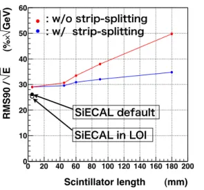
Figure 13. Scintillator ECAL second generation prototype Scintillator length (mm) 0 20 40 60 80 100 120 140 160 180 200 ) GeV ! (% E RMS90 / 0 10 20 30 40 50 60 : w/ strip-splitting : w/o strip-splitting SiECAL default SiECAL in LOI
Figure 14. Strip clustering perfromance: jet energy resolution vs. strip length.
whose directions are orthogonal to the strip under consideration. This algorithms is called Strip-Splitting and found to work well. One of the results is shown in Fig.14, where the jet energy resolutions are plotted as a function of the length of the scintillator strip.
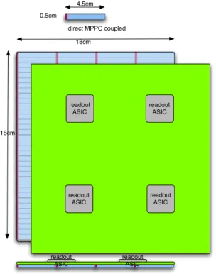
3.2.2 Layer electronics development
A few layers are now under construction, as illustrated in Fig. 15. The scintillator layer will be constructed in Korea and Japan. The electronics layer, with SPIROC ASIC from France, is currently being designed by a DESY engineer and will be incorporated into layers in Japan.
18cm 18cm 4.5cm 0.5cm direct MPPC coupled readout ASIC readout ASIC readout ASIC readout ASIC readout ASIC readout ASIC
Figure 15. Scintillator ECAL second generation integrated read-out electronics layer.
5mm x 45mm x 2mm scinti. MPPC X detected # of photons solid angle & reflec.
Figure 16. Scintillator strip uniformity measured with a Sr-90 source.
3.2.3 5 mm scintillator development
The width of a 5 mm scintillator is expected to be suitable without the use of wave length shifting fibre read out, though homogeneity should be confirmed. This has been tested using collimated90Sr sources, with preliminary results shown in Fig. 16. Relatively good uniformity is measured at x > 5 mm. However, we find non-uniformity due to the acceptance problem in the region near to the photo-sensor. This indicates that further effort is required to achieve optimal response, although in practise the overall energy resolution for electrons and photons are little affected by this non-uniformity.
3.2.4 MPPC development
We now have some MPPCs which consist of 2500 pixels of 20 µm2 within a sensitive area of 1 mm×1 mm. We have tested these devices and found that the new MPPC exhibits an extended dynamic range, and will continue to characterise their response further.
3.3 Future R&D
The integration of layers of scintillator sensors and readout electronics is the next key issue to be address for the current activity. Since this task is also a combination of several countr (Korea, Germany, France and Japan), international effort for the ILC/ILD will play an important role to achieve it.
4. Digital ECAL: DECAL 4.1 Context
The studies of a digital ECAL (DECAL) continue in the UK, in spite of very significant funding difficulties. In Dec. 2008, the STFC Executive recommended sufficient funding to allow the SPiDER Collaboration to construct a full physics prototype DECAL, as outlined in [2]. By Dec. 2009, the funding for SPiDER had still not been issued and STFC informed the Collaboration that they would not do so.
The UK groups in SPiDER have demonstrated that the INMAPS technology developed specifically for the DE-CAL application is viable in terms of basic pixel efficiency. INMAPS is implemented as a 0.18µm CMOS process in which a deep P-well implant stops signal charge from being absorbed in N-well circuits, and therefore allows the use of both NMOS and PMOS within the pixel, as well as (optionally) high resistivity silicon in the thin epitaxial layer to reduce the charge collection time.
4.2 Testbeams in 2010
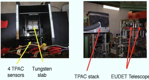
Following a successful test beam run at CERN in Sep. 2009 using 120 GeV pions, two further data taking runs have been carried out. The first of these was at DESY in Mar. 2010, for which the primary goal was to quantify the peak electromagnetic shower density observed downstream of specific absorber materials. A secondary goal was to make further pixel efficiency measurements. Data were recorded with the 1–5 GeV electron beam, using a configuration in
Figure 17. The DESY 2010 testbeam: (left) test stand, showing four upstream sensors and tungsten absorber, and (right) test stand with cooling system and EUDET telescrope upstream.
which four TPAC 1.2 sensors were aligned precisely along the beam direction using the same custom-built mechanical frame as at CERN. Absorber material (W, Fe, Cu) was placed downstream of these, followed immediately by a further pair of TPAC sensors, to study the shower density. The EUDET telescope was located upstream of the DECAL test stand, as shown in Figure 17.
To complement the DESY run, similar, additional data was recorded at CERN in Sep. 2010, using the EUDET telescope alone as it has finer pitch than the TPAC sensor, with positrons between 10 and 100 GeV. Similar absorber
materials and thicknesses to those at DESY were used. Analysis of these data is ongoing, with the aim of having first results to present at TIPP’11 in June.
4.3 Pixel efficiency results
The studies of pixel efficiency from CERN 2009 testbeam and DESY were performed using a set of six TPAC 1.2 sensors aligned along the beam direction, in which the outer four sensors served as a beam telescope, while the two innermost sensors were considered as the devices under test. The trajectory of the beam particle was projected onto the plane of both of these pixels, and each pixel of the test sensors was examined for the presence of hits as a function of the distance from the projected track. The MIP hit efficiency was determined by fitting the distribution of hit probability to a flat top function, convoluted with a gaussion of the appropriate resolution to allow for finite tracking performance. This efficiency, folded for all pixels together, is illustrated in Figure18.
Figure 18. (left) Distribution of the probability of a pixel registering a hit in response to a MIP, as a function of distance to the projected track, and (right) MIP efficiency as a function of the sensor digital threshold, for all four sensor variants studied.
The MIP efficiency was determined per pixel for both the DESY and CERN data, and for each of the four pixel variants tested. The variants (and corresponding marker colour in Figure 18) are:
1. (red) in 12µm standard (non-INMAPS) CMOS;
2. (black) 12µm deep P-well CMOS;
3. (green) deep P-well within a 12µm high resistivity epitaxial layer;
4. (blue) deep P-well within an 18µm high resistivity epitaxial layer.
The results [3] are summarised in Figure 18, for a range of the sensor digital thresholds representative of the signal levels expected in DECAL pixels due to charge spreading. (A typical MIP signal in a 12µm epitaxial layer of silicon is 1200 electrons and a single absorbs at most 50% of this due to charge spreading.)
From the results shown in the figure, it is observed that the standard, non-INMAPS sensors have markedly low efficiencies, which is attributed to signal charge being absorbed by in-pixel PMOS transistors. In contrast, the use of the deep P-well reduces the absorption of signal charge by N-wells in the circuitry, improving very substantially the pixel efficiency by a factor of ∼ 5. The addition of the high resistivity epitaxial layer further improves the pixel efficiency to ∼ 100%.
4.4 Future plans
It is no longer an option to plan for a physics prototype DECAL and the short-term future of the DECAL project is extremely uncertain at present. A programme of radiation hardness testing is in progress during 2011, using X-ray sources at RAL, and may be extended to include neutrons and protons. This is in part to understand how the TPAC
Figure 19. Electronics integration architecture for the technological AHCAL prototype.
sensor would satisfy the requirements of SuperB and ALICE ITS. The technology development will continue while this is still possible. The studies which have been carried out so far are in the process of being finalised, and a series of papers, e.g. [4], are in preparation to document what has been achieved.
5. Analogue HCAL Technological Prototype
A technological prototype of a highly granular scintillator based AHCAL is under design and construction to demon-strated the feasibility of this approach in a realistic linear collider (LC) detector. The challenge is the high level of integration to maintain maximum compactness and hermeticity of the final detector, once the AHCAL design is realized as a whole barrel detector for a LC experiment.
The envisaged detector architecture [5, 6] is sketched in Fig. 19. It is inspired by one variant of the ILD detector concept, but is very similar to those envisaged for SiD or CLIC.
The barrel of the AHCAL has a cylindrical structure and will be placed outside the electromagnetic calorimeter, while it is surrounded by the magnet. The cylindrical structure is divided into 16 segments with 48 detector layers each. The figure shows one sector of a barrel subdivided only once along the beam axis. This layout provides access to electronics and service interfaces once the detector end-cap is opened, but poses tight space constraints to the barrel end-cap transition region.
One active layer consists of three parallel slabs. Each slab is again subdivided in six HCAL basic units (HBU) and the middle slab is connected to the DAQ via the Central Interface Board (CIB). The side slabs are in turn connected to the CIB via the Side Interface Boards (SIBs).
The first HBU module, along with the interface modules, is shown in Fig. 20 left, as it is used in the DESY test setups. In the final design the HBUs are interconnected by flexleads and ultra-thin connectors with a stacking height of 0.8 mm (see Fig. 20 right), which are also used to connect the HBUs to the CIB.
5.1 Tiles and ASICs
The signal that is detected by the SiPMs is produced by scintillating tiles with a size of 3 × 3 × 0.3 cm3, as shown in Fig. 21 left. The new design differs from the design used in the physics prototype [7] and includes a straight wavelength shifting fiber coupled to a SiPM with a size of 1.27 mm2 on one side and to a mirror on the other side. The SiPM comprises 796 pixels with a gain of ∼ 106. Two alignment pins are used to connect the tiles to the HBU’s printed circuit board (PCB) by plugging them into holes in the PCB. The nominal tile distance is 100 µm.
For each HBU the analog signals from the SiPMs are read out by four 36-channel ASICs equipped with 5 V DACs for a channel-wise bias voltage adjustment. They provide two gain modes, which leads to a dynamic range of 1 to 2000 photo electrons. The chips are designed to operate with pulsed power supply for minimized heat dissipation. The foreseen power consumption amounts to 25 µW per channel for the final LC operation. The main new features of the ASICs compared to the physics prototype are the integration of the digitization step (12-bit ADC and 12-bit TDC for charge and time measurements) and the self-triggering capability with an adjustable threshold, which acts as a on-detector zero suppression. To reduce the height of the active layers the ASICs are lowered into the PCB by ∼ 500 µm. This leads to a total reduction of the AHCAL diameter of 48 mm. A picture of an ASIC as it is embedded into the PCB is shown in Fig.21 right.
5.2 Detector/DAQ interface
Fig. 22 shows the cross section of one AHCAL layer including the dimensions of the single components. The active layers, including the tiles, SiPMs, PCBs and ASICs, are shown as they are placed between two layers of absorber material and connected to the CIB. The total height of the detector/DAQ interface modules hosted by the CIB has to be very small (∼ 18 mm in case of a tungsten absorber) in order to fit between two layers.
In Fig. 23 the electronics setup is shown in the final assembly stage: The DAQ interface modules DIF, CALIB2 and POWER2 are realized as mezzanine cards on top of the central-interface board (CIB). All modules fulfill the stringent space requirements for an arrangement in the pitch of the absorber plates. All DAQ interface modules have been realized and are in commissioning stage at the moment. The module DIF has been realized by the Northern Illinois University (NIU). It serves as the interface between the inner detector module (HBU) and the back-end DAQ. The CALIB2 module controls the light calibration and gain monitoring system for the SiPMs, which is based on the usage of ultraviolet LEDs. The POWER2 module provides all necessary supply voltages to the inner detector electronics, including the SiPM bias voltages. Additionally, it enables the power-cycling of the HBU electronics in the scheme of the ILC bunch-trains. The final HBU module with the newest generation of readout ASICs SPIROC2b is currently in production.
Up to 10 CIB modules can be connected to one Link and Data Aggregator (LDA) module of the final CALICE DAQ. The LDA collects the parallel incoming data streams of the DIFs on the CIB modules, and serializes the data to a single, duplex optical line, which connects to the backend DAQ (ODR module, not shown in Fig. 23). Timing critical signals as the front-end clock, which is used by all front-end modules for a synchronous operation of all detector parts, are provided from the central experiment through the Clock-and-Control module (C&C). In testbeam setups, the C&C module can be used for the distribution of a fast trigger as well. The setup as shown in Fig. 23 is still in the beginning of the commissioning phase, the prototype has been operated so far by a preliminary Labview DAQ via an USB connection between a PC and the DIF-module.
Figure 20. Left) Current setup of an HBU as used in the DESY test measurements. Right) HBU interconnection via flexleads and ultra-thin connectors.
Figure 21. Left) Scintillating tile with embedded wavelength shifting fiber, SiPM, mirror and alignment pins. Right) Integration of the SPIROC ASIC into the PCB.
Figure 22. Cross section of one HCAL layer, including the absorbers, tiles, SiPMs, PCBs, ASICs and the detector/DAQ interface modules. All dimensions are given in mm.
Figure 23. Electronics setup of the inner detector electronics (HBU) connected to the DAQ interface modules (DIF, CALIB2 and POWER2) via the flexleads and the CIB module, and together with the final CALICE DAQ modules LDA and C&C. The setup is not yet in operation, but still in commissioning phase.
5.3 Light calibration system
Since the SiPM response shows a strong dependence on the temperature and bias voltage and saturates due to the limited number of pixels, a gain-calibration and saturation-monitoring system with a high dynamic range is needed. In the calibration mode of the ASICs a very low light intensity is needed to measure the gain as the distance between the peaks in a single-pixel spectrum, while at high light intensities (corresponding to ∼100 minimum-ionizing particles (MIPs)) the SiPM shows saturation behavior. Currently there are two concepts under investigation:
Figure 24. Left) Measurement result of a typical MIP spectrum obtained with the HBU and the DAQ interface modules using the newly developed Labview/USB DAQ in the 6 GeV DESY electron testbeam. Right) Light yield as measured in the DESY testbeam facility for multiple channels of the HBU.
• One LED per tile that is integrated into the detector gap. This system is used in the HBUs in the DESY test setups.
• One strong LED outside the detector, while the light is distributed to each tile via notched fibers (see [8]).
Both options have been successfully tested on the DESY test setups in the laboratory and under testbeam con-ditions. The measured cross-talk is purely optical and is of the order of 2.5%. The dynamic range of the system redesigned for the construction of the engineering prototype is currently under investigation. The channel uniformity is also an open issue, since for the first LED system the individual LEDs have a large spread of the emitted light intensity, while for the second system the light coupling from the fiber to the tile and its mechanical integration in a full prototype is unsolved.
5.4 Measurements and results
The main task of the current characterization is to prove the suitability of the realized detector-module concept for the larger-scale prototype with 2500 channels and the final length of 2.2 m. Two HBUs are in operation, one in the DESY 6 GeV electron testbeam facility (the 2-6 GeV electrons that have been used are MIPs in the scintillating tiles) and the second in a laboratory environment.
After the investigation of the fundamental properties of the SPIROC chip like noise behavior and signal delays [9], measurements in the laboratory using the LED calibration system and a charge injection setup, as well as testbeam measurements have been performed to investigate the uniformity of the tile/SiPM response for multiple channels. Fig. 24 left shows a typical MIP spectrum measured with the electron testbeam. It can be seen that single pixel peaks are clearly distinguishable for more than 10 peaks. The first peak is the pedestal peak and the maximum of the spectrum is at 9 pixels. The distribution of the light yields, defined as the most probable number of active pixels for a MIP signal, is plotted in Fig. 24 right.
The auto-triggering function of the SPIROC chip has been tested [10]. Fig. 25 left shows two single-pixel spectra measured with LED light and external trigger (black histogram) and auto-trigger (red histogram), respectively. The ratio of the two histograms is also shown and gives an impression of the width of the trigger turn-on curve. After the turn-on the trigger efficiency is 100%.
The threshold of the auto-trigger will be adjusted in order to minimize the noise hits and simultaneously maximize the efficiency for measuring a MIP.
For a threshold requirements of less then than 10−4noise hits per event, one gets a MIP efficiency of around 95% as illustrated in Fig. 25 right.
Figure 25. Left) Comparison of a single-pixel spectrum produced with LED light for external- and auto-triggering with a given threshold. Right) Calculated auto-trigger threshold for having a noise to signal ratio of smaller than 10−4. An independent pedestal measurement is compared to a MIP spectrum.
Here the noise threshold is fixed with respect to the pedestal distribution for one given channel (black histogram) and the MIP detection efficiency is calculated from the MIP distribution (red histogram) of the same channels. 5.5 Future plans
In 2011, the system will be further commissioned, including also the timing functionality.In parallel, final versions of the read-out and interface boards are in production, With this, all components are in hand for a multi-module layer tests, using the tile sand new sensors under production at ITEP.
For 2012 a multi-layer test is planned where several options are possible. The HBUs can be arranged in a flexible manner, such that one can instrument an electromagnetic section if the stainless steel module (a tower of 12 HBUs), or produce a few larger area layers (two by tow HBUs) to start exploring time-resolved 4-dimensional shower mea-surements in the tungsten HCAL. Provided sufficient funding, the second generation prototype will be extended to 40 hadronic layers.
6. Tungsten Analogue HCAL: W-AHCAL 6.1 Motivation
A hadron calorimeter required for the multi-TeV range of the CLIC linear collider will have to cope with increased jet energies. Particle separation will become more difficult and confusion will be of increased importance in the detector resolution when particle flow algorithm is used. But also leakage will be an important contribution to the energy resolution. In the design of the detectors proposed for CLIC a depth of the hadron calorimeter of 7.5 λI is required.
The calorimeter has also to be placed inside the solenoid to achieve optimum resolution. Iron (λI = 16.77 cm) as
absorber would yield then to a larger radius for the solenoid, which would be costly and difficult to realize. The choice of an heavier absorber material like tungsten (λI= 9.95 cm) leads to a substantially smaller solenoid diameter.
However, tungsten needs to be validated as absorber material. A particular question is the influence of delayed neutrons produced by spallation of the tungsten on the shower development. Also the simulation of the hadronic shower development in tungsten has not yet been validated to the same precision as the one in iron as absorber. Therefore a sampling calorimeter has been built using a tungsten absorber and scintillator tiles as readout with a total depth of 4.9 λI. First experimental data have been taken using a calorimeter depth of 3.9 λI.
6.2 Experimental prototype
The W-HCAL prototype has been designed in order to use the scintillator cassettes built for the AHCAL physics prototype [7]. The material used in the absorber was a sintered alloy formed by 93% W, 5.3% Ni and 1.7% Cu. This
alloy allows easy machining and handling since it is much less brittle then pure tungsten. Each absorber layer has been assembled from 5 square tungsten plates of 27 × 27 × 1 cm3 size and 4 triangular plates with corresponding size to form an octagon with 81 cm diameter (see Fig.26, left).
Figure 26. View of W-HCAL absorber plates (left) and stack during assembly(right).
This octagon has been glued into an aluminum frame of a size of 1 × 1 m2. For stability reasons the assembly has been glued to a 0.5 mm thick and 1 m2 sized stainless steel plate. Forty layers with an absorber thickness of 10 mm each have in total been assembled. Thirty and of these layers have been constructed in 2010 and another ten in 2011. The first thirty layers have been assembled in a stack with an interleaving space of 14 mm in between successive absorber layers leaving room for scintillator tile cassettes as active modules (see Fig. 26, right). Each cassette contains 216 scintillator tiles with a thickness of 5 mm: In the central core of the detector are situated 100 tiles with a size of 3 × 3 cm2, surrounded by 96 tiles sized 6 × 6 cm2. As can be seen in Fig. 27, left, cells with a size of 12 × 12 cm2are arranged on the very outside of the cassette.
Figure 27. Scintillator tiles layer (left), assembled module with front end electronics (right).
Each tile is read out individually via a wavelength shifting fibre coupled to a silicon photomultiplier (SiPM) mounted on the tile. The SiPM is a multi-pixel avalanche photodiode operated in Geiger mode and provides a gain of more than 105. The scintillator tile layers and the read-out are the same used already in the AHCAL tests with steel absorber in the previous test beams at DESY (2006), CERN (2007) and FNAL (2008, 2009).
The front end electronics is mounted on one side of the cassettes (see Fig. 27, right). It is based on 16 channel ASICs which are read out by the standard CALICE DAQ system. For the calibration and equalization of all the detector channel, test bench characterizations as well as test beam data are used. The detailed procedure is described elsewhere [7].
Minimum ionizing muon beams were used to equalize the cell response. All the cells are equipped with an LED illumination to monitor the gain of each of the SiPMs. In addition the SiPM temperature and SiPM bias voltage have been monitored. Detailed studies of the applied temperature offset corrections were performed.
Figure 28. Example of muon (left) and pion (right) event displays in the W-HCAL, for a beam energy of 8 GeV. The prototype, equipped with thirty layers of tungsten absorber, has been put into the CERN-PS. About 28 million triggers have been taken using e±, µ±, π±and protons in the energy range of 1 to 10 GeV. The beam passed through 2 threshold Cherenkov counters placed upstream in the beam which were used for offline particle identification. Typical events of muon and pions are shown in Fig.28.
In Fig. 29, left, the energy sum of the total calorimeter is plotted for positrons, muons, pion and protons at 5 GeV. The beam is always contaminated with muons which behave as minimum ionizing particles. Therefore the muon peak is well distinguished for beam energies Ebeam≥ 3 GeV. In Fig. 29, right, are plotted the calorimeter reponse of muons
and pions for energies varying from 1 to 10 GeV.
Figure 29. Total energy deposited in the W-HCAL: (left) 5 GeV positrons, pions and protons; (right) Muon and pion peaks for beam energies from 1 to 10 GeV.
Note that the presented results still use old calibration data (from CERN 2007). However, a first look at the new MIP calibrations indicates very similar calibration values.
We foresee to extend the test in 2011 to an energy range of up to 300 GeV at the CERN-SPS accelerator. From energies of approximately 60 GeV onwards, transversal leakage will become an important contribution to the observed
1000 mm
435 mm
1 2 3 4 5 6 7 8 9
10 11 12 13 14
0
Figure 30. Layout of the T3B scintillator tiles. From the nominal beam axis, the setup extends by 15 mm to one and 435 mm to the other side.
resolution. In order to cope with this, it is planned to add an instrumented tail catcher with a thickness of 6 λI behind
the calorimeter.
6.3 T3B: Time Structure of Hadronic Showers in the W-AHCAL
For calorimeters in CLIC detectors, the time stamping capabilities are of significant importance because of the high bunch crossing frequency of 2 GHz and the high hadronic background from γγ → hadrons processes. For hadronic showers, the possible time resolution is not only given by the active detector elements, but may well be limited by the intrinsic time structure of the showers themselves. For absorbers with heavy nuclei, such as tungsten, a particularly complex time structure is expected, calling for experimental verification of this aspect of the detector simulations.
To provide first experimental input, a specialized experiment, the Tungsten Timing Test Beam (T3B) detector, was developed and installed in the tungsten analogue HCAL (WHCAL) prototype. A first data taking period at the CERN PS in November 2010 was successfully completed, providing first analysis results [11] that constrain Geant4 physics lists.
6.3.1 T3B: setup and data analysis
The T3B setup consists of fifteen 3 × 3 cm2scintillator tiles with a thickness of 5 mm, directly read out with 1 mm2 Hamamatsu MPPC50P SiPMs with four hundred 50 × 50 µm2pixels. The scintillator tiles have a “dimple” drilled into the side face at the SiPM coupling position to achieve a uniform response over the full active area [12]. At nominal operation, they provide a signal of approximately 27 photoelectrons (p.e.) for minimum ionizing particles, including afterpulses of the photon sensor.
The photon sensors are read out with 4-channel USB oscilloscopes1with 1.25 GS per second, using long acquisi-tion windows of 2.4 µs per event to record the time structure of the energy deposits in the scintillator in detail. Each SiPM was connected to a preamplifier board, which then feeds the signal to the oscilloscope via coaxial cable. The preamplifier boards with packaged scintillator cells were mounted on a 2 mm thick aluminum plate and protected by a 1 mm thick aluminum top cover, forming a robust cassette.
The T3B scintillator tiles are arranged in one row extending from the center of the calorimeter layer out to one side of the detector. The first tile is centered on the nominal beam position, thus the setup extends 15 mm beyond the nominal beam center on one and 435 mm on the other side, as shown in Figure 30. This permits the measurement of a full radial timing profile of the hadronic shower at the position of T3B, given sufficient statistics. The limited coverage however only allows averages over many events to be measured, and is not suitable for the study of the time evolution on an event by event basis.
A first analysis of 645 000 10 GeV π−events was performed, using T3B in standalone mode without attempting to correlate the events with CALICE WHCAL events to obtain additional information about the showers. The data were analyzed on a cell by cell level. As a first step, zero suppression based on pedestals determined on a spill-by-spill basis was applied. Then, waveforms with an integral above 0.3 MIP were decomposed into individual photon equivalents to provide precise information on the arrival time of photons at the light sensor. This was done by consecutively
time [ns] 300 350 400 450 500 550 signal amplitude [V] 0 0.02 0.04 0.06 0.08 0.1 0.12
signal amplitude [p.e.]
0 1 2 3 4 5 6
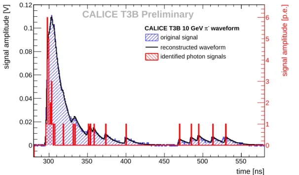
CALICE T3B Preliminary
waveform -π CALICE T3B 10 GeV original signal reconstructed waveform identified photon signalsFigure 31. Typical waveform with a high initial signal, decomposed into individual photon signals during the data analysis. Very good agreement of the original waveform and the reconstructed signal from standard single photo-electron distributions is observed.
subtracting single photon signals from local maxima detected in the waveform, until no maxima above approximately 0.5 p.e. remained. The single photon signals were obtained from noise events taken between spills and are determined for each tile separately. This results in an implicit gain calibration, since possible cell-to-cell gain differences lead to corresponding differences in the average single photon signals used in the analysis. The resulting number of photons is thus independent of the SiPM gain. This reference signal was refreshed every 10 spills, typically corresponding to time intervals of less than 5 minutes. This provided continuous automatic corrections of gain variations due to temperature changes.
Figure 31 shows one example of a waveform decomposed using this reconstruction technique. To check the
quality of this analysis, a waveform based on the identified photon signals was built up with the reference single photon signals and compared to the original waveform. The very good agreement between measurement and the reconstructed waveform demonstrates the quality of reconstruction. First results using this reconstruction are outlined in Sect. 11 below.
7. Digital HCAL: DHCAL
The Digital Hadron Calorimeter Project trades the typical tower structure of past hadron calorimeters and their high-resolution readout with large number of finely segmented active elements, read out individually with a single bit resolution.
7.1 RPC-based DHCAL 7.1.1 Description of the project
A collaboration of institutes (Argonne, Boston, FNAL, IHEP Beijing, Iowa, McGill, Northwestern, and Texas at Arlington) is developing such a novel calorimeter with Resistive Plate Chambers (RPCs) as active media. Currently the readout is segmented into 1 × 1 cm2pads or 10 000 per square metre.
The project progressed in several stages. In a first stage, different designs of RPCs were developed and tested with a high-resolution readout system [13]. In parallel to this activity a 1-bit readout system capable of handling large numbers of channels in a cost-effective way was developed. The second stage put the two together in a small prototype
calorimeter, here named the Vertical Slice Test (VST), and included detailed tests with both cosmic rays and in the Fermilab test beam. For the first time within the CALICE collaboration the VST utilized a readout system with the digitization taking place directly on the front-end boards. Based on the successful experience with the VST [14, 15, 16, 17, 18] and after a further round of R&D, the third stage consisted of the construction of a large technical prototype hadron calorimeter (the DHCAL) with, close to 350 000 readout channels. The active elements were inserted into the CALICE hadron calorimeter absorber structure. The calorimeter is now undergoing tests in the Fermilab test beam.
Located behind the hadron calorimeter is the CALICE Tail Catcher and Muon Tracker (TCMT) with 16 active layers. Over the past six month its Scintillator layers have been gradually replaced with RPC layers, identical to the one’s in the DHCAL. This brought the total number of readout channels of the combined DHCAL + TCMT system to approximately 480 000.
Following the tests in the Fermilab test beam, the DHCAL group will return to R&D to tackle the remaining technical issues in preparation of the construction of a so-called Module 0.
Additional information pertaining to this project can be obtained from [19].
7.1.2 Past achievements since the last review
The DHCAL group has been very active since the last review: publishing papers, completing the R&D necessary for the construction of the DHCAL, constructing the DHCAL and the RPC-TCMT, installing the active layers into the CALICE structures in the Fermilab test beam, taking data with various beam configurations, and last but not least analyzing the collected data. In the following we provide a few additional details on these activities:
Completion of the analysis of the VST data. The 5thand last paper based on data from the VST was published in JINST and documented the environmental dependence of the performance of RPCs.
R&D in preparation of the construction of the DHCAL Moving from the VST to the DHCAL represented an increase in size and channel count of roughly a factor of 200. Techniques to spray the glass plates with resistive paint providing the required surface resistivity and homogeneity were developed. Fixtures for the preparation of the rims of the RPCs were designed, built and optimized. Three identical fixtures for the assembly of RPCs were built. In order to provide the required uniformity of the gas gap, the fixtures were machined with a precision better than 0.1 mm.
The application of high voltage posed a significant problem, as an attempt was made to minimize the inactive rim around the edge of the chambers. After several set-backs we developed a technique which allowed us to extend the resistive paint up to within a couple of mm from the edge, without the risk of a high voltage break down.
The readout boards consist of a pad board (each with 1536 pads of 1 × 1 cm2) and the corresponding Front-end board (with 24 DCAL ASICs), thus avoiding the need for costly blind vias. The two boards are mated to together by applying drops of conductive glue on glue pads on the back side of the pad board. A gluing fixture was designed and built to apply the 1536 glue dots in a timely fashion.
Several prototype iterations were necessary before embarking on the mass production of the front-end boards. The challenge was to minimize the cross-talk between the digital activity of the board and the analog front-ends.
Finally, a viable design of the detector cassette needed to be developed. The role of the cassettes is to: (i) provide a mechanical structure to hold the 3 RPCs in a given layer together, and (ii) to provide a surface to cool the front-end ASICs. Our cassette design exerts slight pressure on the front-end boards against the underlying RPC. This is required to minimize the distance between the two and therefore to reduce the average pad multiplicity for single Minimum Ionizing Particles (MIPs).
Construction of the DHCAL and RPC-TCMT The construction of the DHCAL and RPC-TCMT took approxi-mately two years and involved up to 15 people at a given time.
Over 700 sheets of glass were sprayed with resistive paint. The procedure was never completely under our control and the efficiency was only about 60%. We made no effort in controlling the environment and abrupt changes in the weather typically required a tedious re-tuning of the various parameters of the spraying gun.
205 RPCs (with the dimensions of 32 × 96 cm2) were produced in three parallel assembly lines. The gap size was maintained at a very uniform level, with slightly larger values (<100 µm) at the four corners. The chambers were
tested for gas tightness and the high voltage connections were added. The chambers typically operate at 6.3 kV, but were tested overnight at 7.0 kV.
Over 300 Front-end boards and pad boards were produced. The boards were checked out thoroughly in three test stations, working in parallel. Each test took between 3–6 hours. Faulty boards, with e.g. more than 4 dead channels, were repaired and retested.
Cassettes consisting of a 2 mm copper matched by a 2 mm steel cover, a top and a bottom bar were produced by an outside company. The assembly of the cassettes was relatively straightforward and could be accomplished in less than one hour per cassette.
Of the order of 50 Data collector modules were built and tested at Boston University. Again a dedicated test station was needed to check out the boards. Twelve Timing and Trigger Modules were fabricated and assembled. The check out was done at Fermilab.
New gas mixing and distribution racks were built and commissioned. The RPCs require a mixture of three gases (Freon, Isobutan and SF6). The distribution rack features 28 outputs with individual controls.
The Front-end boards require +5 V. A low voltage power supply system was built which uses commercial Wiener power supplies and custom made distribution boxes. The system provides low voltage to all 306 front-end boards of the combined DHCAL and TCMT system. Each line can be individually controlled and is separately fused.
The high voltage system is on loan from CERN and Fermilab. Due to its relative old age (from the early 1980s), the system is prone to frequent break downs. The group is considering replacing the system with a commercially available system.
The completed cassettes were transported from Argonne to Fermilab in a specially devised transport structure, which minimized the impact of shocks due to bumps on the road. The cassettes were inserted into the CALICE Hadron Calorimeter absorber structure and into the CALICE TCMT. Fig.32 shows photographs of the two structures after installation of the RPC layers.
Figure 32. Photograph of the DHCAL (left) and the RPC-TCMT (right). The photos were taken before (after) cabling of the DHCAL (RPC-TCMT).
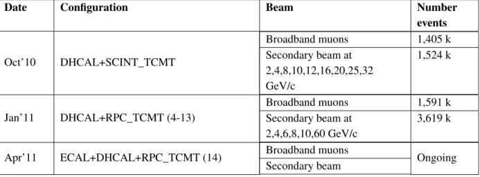
Data taking at Fermilab Testing of the DHCAL in the Fermilab test beam started in October 2010. Table I summa-rizes the data taken since. In general the data are of very high quality. The broadband muons were obtained with the 32 GeV/c secondary beam and a 3 meter long iron beam blocker.
As the January run progressed we gradually replaced the Scintillator TCMT layers with RPC layers identical to the ones in the DHCAL. In Tab. 1. the number of RPC – TCMT layers is indicated in parenthesis.
In its current and final configuration the system counts 480 000 readout channels. In April 2011 the CALICE Silicon-Tungsten electromagnetic calorimeter was installed in front of the DHCAL, bringing the total number of read-out channels to 490 000.
Date Configuration Beam Number events Oct’10 DHCAL+SCINT_TCMT Broadband muons 1,405 k Secondary beam at 2,4,8,10,12,16,20,25,32 GeV/c 1,524 k Jan’11 DHCAL+RPC_TCMT (4-13) Broadband muons 1,591 k Secondary beam at 2,4,6,8,10,60 GeV/c 3,619 k
Apr’11 ECAL+DHCAL+RPC_TCMT (14) Broadband muons
Secondary beam Ongoing
Table 1. Summary of the DHCAL data taking at the Fermilab test beam facility.
Due to the rate limitation of RPCs, pion and positron events are collected simultaneously. Separate data sample are generated offline using the Cerenkov signal.
7.1.3 First DHCAL results
A rigorous effort is underway to analyze the DHCAL data in a timely manner. Due to the fact that the data have been collected quite recently, the results shown here are still preliminary. In order to provide a flavor for the ongoing activities, in the following, we sample results from different analysis efforts. Additional results can be obtained from
the DHCAL CALICE notes [20, 21, 22].
1. Analysis of cosmic ray data. The completed chambers were inserted into a cosmic ray test stand and tested with cosmic rays. The stand could accommodate up to nine chambers at a given time. As an example, Fig. 33 shows the distribution of cosmic rays, the efficiency and the pad multiplicity as a function of the dip angle of the cosmic rays.
2. Measurement of the noise rate. The noise rate is measured two ways: i) in trigger-less operation, where any hit in the detector is recorded and ii) in triggered operation during off-beam times, where the trigger is provided by a pulse generator. The two methods are seen to provide consistent results [20]. Fig. 34 shows the noise rate as function of layer number or of RPC number. The average noise rate of 0.6 Hz/cm2 is somewhat elevated for this type of detector and due to the elevated temperature in the stack. Nevertheless, the measured noise rate contributes in average only 0.06 hits or 4 MeV per triggered event.
3. Analysis of muons. Muons are used to geometrically align the layers in the stack and to measure and monitor the performance of the calorimeter [21]. Fig. 35 shows the MIP detection efficiency, the average pad multiplicity and the calibration factors as function of layer number.
4. Analysis of secondary beam data. Fig. 36 shows the event display of a 60 GeV pion with significant leakage into the RPC-TCMT. Note that the observed isolated hits are not originating from noise, but are generated by the hadronic shower. Some first results based on events like this are outlined in Sect. 11 below.
7.1.4 Future plans
In parallel to the large effort of assembling the technical prototype the collaboration has initiated R&D related to the remaining technical issues of an RPC-based hadron calorimeter. Tab. 2 summarizes the various ongoing and planned activities.
Figure 33. Distribution of cosmic rays, average pad multiplicity and MIP detection efficiency as function of the dip angle of cosmic rays.
Figure 34. Noise rate in Hz/cm2as function of layer number and as function of RPC number. The different colors correspond to
different runs taken at different times.
7.2 GEM-based DHCAL
7.2.1 GEM 30 cm × 30 cm prototype tests with KPiX readout system
Figure 35. MIP detection efficiency, average pad multiplicity and calibration factors as function of detector layer as measured with broadband muons.
Figure 36. Display of a 60 GeV pion event with significant leakage into the RPC-TCMT. The observed isolated hits are part of the hadronic shower and are not due to noise.
R&D topic Funds Comment
Thin RPC Applied for Further investigation of 1-glass design
Large area RPCs Currently not
pursued
Areas of several m2needed
Gas system Funded Exploration of new gas mixtures, recycling, gas
distribu-tion High Voltage
distri-bution
Funded System capable of supplying HV to all layers of a
mod-ule individually Low Voltage
distri-bution
Currently not pursued
System capable of supplying LV to all layers of a module individually
Wedge shape Currently not
pursued
Develop concept to accommodate wedge shaped module designs
Pad/FE-board Currently not
pursued
Develop new design which minimizes thickness
Front-end ASIC (Funded) Develop next iteration with reduced power consumption,
token ring passing, and redundancy for reliability
Data concentrator Currently not
pursued
Develop new system which minimizes space require-ment and provides high reliability
Mechanical
struc-ture
Currently not pursued
Develop cassette structure which can be oriented which ever way, develop module structure which accommo-dates all supplies and data lines
Magnetic field Currently not
pursued
Tests of all subsystems in magnetic field
Table 2. Summary of R&D topics beyond the construction of the technical prototype.
was designed. In order to use the prototype chamber for beam tests and for integration of KPiX Analog and DCAL digital readout systems, we constructed three of these chambers. After completing one of these new chambers, with the new gas-transparent G10 spacer from CERN and the updated KPiX readout board, we performed source tests using
55Fe and106Ru radioactive sources. Since55Fe has characteristic peaks from 5.9 keV and 4 keV X-rays losing their
entire energy in the chamber, it provides an excellent test for chamber performance.
Fig.37 (a) shows two distinct peaks from55Fe X-rays in channel 49. The source particles were narrowly col-limated to ensure that the particles traversed a normal incidence path rather than with large incident angles. After confirming the minimum ionizing particle pulse height distributions from106Ru β source which shows the typical MIP Landau distributions, we moved into two dimensional measurement by removing the collimator. The source particles are then able to go through various channels demonstrating two dimensional profile distributions in Fig. 37 (b). Fig. 37 (c) shows the characteristic Landau distributions from cosmic ray muons obtained through the 2 cm × 2 cm coinci-dence trigger coverage and plotting the charges from the highest charge pad. Fig. 37 (d) shows the lego plot of the hits from the cosmic ray muons, clearly showing the area covered by the trigger paddles.
We are now in the process of investigating uniformity of the chamber responses by performing response mea-surements in many different channels. We do see some implication of differences in channel gains a factor of 3.5, we believe this is caused by incorrect application of electronic gains correction in KPiX software. We believe we will resolve this issue shortly working with the SLAC team. Once these issues are resolved, we will be able to deter-mine chamber gains using sources and will take cosmic ray data for further MIP studies and efficiency studies. We will then, as described in detail in the next section, take the chamber to a particle beam for high statistics chamber characterization.
Figure 37. (a) Pulse height distributions from55Fe source, showing characteristic peaks from 5.9 keV and 4 keV X-rays (b) Lego
plot of hits in all active channels with radioactive source (c) Pulse height distribution from cosmic ray muons, conforming to a Landau distribution (d) Lego plot of hits from cosmic ray muons which conforms to the trigger coverage area
7.2.2 Pressure dependence corrections
Due to the recirculation setup of the Ar-CO2gas, our GEM chamber gains depend on the atmospheric pressure. We
have observed the changes in chamber results over a period in which the atmospheric pressure was known to be changing. Therefore, it is of critical importance for chamber characterization, the chamber gains are corrected for pressure dependence. This section describes the pressure dependence correction.
The measurement was performed using a 30 cm × 30 cm GEM prototype chamber read out through the 64 channel KPiX7 chip. The electronics was comprised of two low voltage power supplies, both set at 7 A; one for the FPGA board and another located for the interface board. The GEM detector is directly connected to a high voltage power supply, which is used to set the potentials between the GEM foils. To study pressure dependence, a55Fe source was elevated a distance above the GEM window and is centered in relation to the readout pads. The pressure dependence of the chamber was studied by performing hour-long runs. The pressure of the local area (City of Arlington, Texas) can be retrieved from national weather services and for each run; and thus subsequent pressure is recorded.
Each hour-long measurement is then analyzed and fitted with a Gaussian distribution where its peak position (peak charge position) is recorded. After multiple data is obtained, a plot of peak position vs. pressure can be made and a linear-regression line made.
The fitted equation from the regression line is obtained where the dependent variable is gain and the independent variable is pressure. It is used to correct for pressure at 1 atmosphere (atm), which is theoretical gain (gtheo) from the
fit. The ratio of theoretical gain, at all the pressures where data was taken, over the measured gain at 1 atm is used as the correction factor (Cf). Using the theoretical gain equation we can input the pressure of the elapsed time for each
hour interval and combined with the theoretical gain for that interval and obtain the correction factor, as follows:
gtheo= −303.9 p + 35509 → Cf =
gtheo
g1atm