Integrating Atomic Force Microscopy in Scanning Electron Microscopy.
Andrew J. Smith1, Klaus Schock1, Gregor Renka1, Andreas Lieb2, Massoud Dadras3, and Stephan
Kleindiek1
1. Kleindiek Nanotechnik, Reutlingen, Germany
2. Nanosurf AG, Gräubernstrasse 12–14, 4410 Liestal , Switzerland
3. Centre Suisse d’Électronique et de Microtechnique, CSEM SA, Neuchâtel, Switzerland
Combining Atomic Force Microscopy (AFM) with Scanning Electron Microscopy (SEM) opens up new possibilities in 3D imaging. The SEM has the ability to quickly generate images of the sample using a wide array of detectors and analysis methods (SE, EBSD, EDX, ...). These methods can be utilized to locate an area of interest. With an in situ AFM, the located site can be imaged using force microscopy without the need for complicated registration or cumbersome relocating of the area of interest ex situ. In this setup, the AFM cantilever is mounted to a micromanipulator while the sample is mounted to a sample scanner. Thus, once the area of interest has been located as described above, the cantilever can be brought into position and landed on that site. Subsequently, the sample is scanned under the cantilever tip in order to generate a topography image.
With the large amount of current research and development focused on nano wires, carbon nano tubes, and other nano scale materials, imaging these materials has become a large part of the challenges involved.
The two most prominent methods for imaging at the nano scale are Scanning Electron Microscopy and Atomic Force Microscopy. These complimentary methods utilize fundamentally different principles for generating imagery - SEM exploits the interaction of electrons with matter, while AFM is based on physical interaction of a sharp tip with the sample surface.
Both approaches have strengths and weaknesses. The SEM's strength is to quickly generate images with a large range of magnifications, making it easy to locate the area of interest. However, it doesn't yield 3D information, e.g. "invisible" contamination layers. The AFM's main advantage is its ability to obtain 3D information, the downsides are that it is hard to find the target area and image generation is slow. Combining these two tools into one setup - putting an AFM inside an SEM - gives quick access to a more complete data set. Additionally, FIB-milled or FIB-deposited structures can be characterized using this combination of tools in a FIB/SEM system.
The utility of this combination of tools is demonstrated with several examples where locating the area of interest purely by AFM or light microscopy would have been highly impractical.
Paper No. 0716 1435
doi:10.1017/S1431927615007953 © Microscopy Society of America 2015
Microsc. Microanal. 21 (Suppl 3), 2015
https://doi.org/10.1017/S1431927615007953
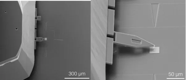
Figure 1. Addressing the target area for AFM inspection is fast and easy using the SEM.
Figure 2. Si surface observation by SEM and AFM characterization of defects. The defects have a
height of about 12nm.
1436 Microsc. Microanal. 21 (Suppl 3), 2015
https://doi.org/10.1017/S1431927615007953