HAL Id: hal-01629904
https://hal.archives-ouvertes.fr/hal-01629904
Submitted on 6 Nov 2017HAL is a multi-disciplinary open access archive for the deposit and dissemination of sci-entific research documents, whether they are pub-lished or not. The documents may come from teaching and research institutions in France or abroad, or from public or private research centers.
L’archive ouverte pluridisciplinaire HAL, est destinée au dépôt et à la diffusion de documents scientifiques de niveau recherche, publiés ou non, émanant des établissements d’enseignement et de recherche français ou étrangers, des laboratoires publics ou privés.
Boron and high-k dielectrics: Possible fourth etch stop
colors for multipattern optical lithography processing
Shailesh Dhungana, Thuong Nguyen, Bradley Nordell, Anthony N. Caruso,
Michelle Paquette, Georges Chollon, William Lanford, Kris Scharfenberger,
Danya Jacob, Sean King
To cite this version:
Shailesh Dhungana, Thuong Nguyen, Bradley Nordell, Anthony N. Caruso, Michelle Paquette, et al.. Boron and high-k dielectrics: Possible fourth etch stop colors for multipattern optical lithography processing. Journal of Vacuum Science and Technology A, American Vacuum Society, 2017, 35 (2), �10.1116/1.4974920�. �hal-01629904�
To be submitted to Journal of Vacuum Science & Technology A
Boron and High-k Dielectrics: Possible Fourth
Etch Stop Colors for Multi-Pattern Optical
Lithography Processing
Running title: Boron and High-k Dielectrics... Running Authors: Dhungana et al
Shailesh Dhungana, Thuong D. Nguyen, Bradley J. Nordell, A. N. Caruso,a) Michelle M. Paquettea), b)
Department of Physics and Astronomy, University of Missouri-Kansas City, Kansas City, MO 64110, USA
Georges Chollon
Laboratoire des Composites Thermotructuraux (CNRS, CEA, Safran, Univ. Bordeaux), 3, allee de La Boetie, Pessac, 33600, France
William A. Lanford
Department of Physics, University at Albany, 1400 Washington Avenue, Albany, NY 12222
Kris Scharfenberger, Danya Jacob, Sean W. Kinga), b)
Logic Technology Development, Intel Corporation, 5200 NE Elam Young Parkway, Hillsboro OR 97124, USA
a)American Vacuum Society member. (Please identify all AVS member authors.) b)Electronic mail: [email protected]; [email protected]
ABSTRACT. In a parallel investigation, the etch characteristics of materials within the Si-C-O-N-H system were surveyed using two common fluorinated plasma etches used to etch SiO2 interlayer dielectrics and SiN:H etch stop layers (CHF3 and CF4/O2,
respectively) with the goal of identifying new materials or “colors” to assist in the simplification of advanced multi-pass optical lithography. In this study, we investigate
2
additional materials outside the traditional Si-C-O-N-H phase diagram with the hope of identifying potential third or fourth color pattern-assist materials. The specific materials investigated include a series of high-k dielectrics commonly used in the industry (Al2O3,
AlN, and HfO2) and boron-based solids (a-B:H, a-BxN:H, a-BxP:H, and a-BxC:H) that
have been previously identified as potential hard mask, polish stop, and/or low-k
dielectric materials. The high-k dielectrics were all found to exhibit low to unmeasureable etch rates in both fluorinated etches. In contrast, the boron-based solids all exhibited etch rates in the CF4/O2 etch an order of magnitude or more higher than those of silicon-based
materials while still exhibiting comparable etch rates in the CHF3 ILD etch. The high-k
dielectrics thus appear to be potential third or fourth color materials, provided etch chemistries capable of selectively etching these relative to other silicon- and carbon-based materials can be identified. In contrast, the results for the boron-carbon-based solids suggest more immediate applications in patterning silicon-based materials. A more detailed examination of the B-C-H system also suggests that significant optimization of the etch selectivity for a-BxC:H can be achieved via compositional tuning for this and
I. INTRODUCTION
New pitch division and multi-pass patterning methods needed for printing <20 nm dimensions require a complex film stack to reduce and transfer the dimensions that can be currently printed in photoresists using 193 nm deep UV immersion lithography.1-3 To some extent, this patterning complexity and the associated materials/etch requirements can be simplified by consideration of the four color map theorem. This theorem states that a geographic map can be painted with just four unique colors such that no two bordering domains share the same color.4 The multi-pattern analogy to this theorem is that only four unique combinations of materials and etches with perfect etch selectivity relative to one another are needed to achieve any conceivable multi-pattern process scheme. However, the unfortunate reality is that the combination of materials and etches commonly available within the semiconductor industry at best only represents two or three colors.5 Thus, additional combinations of materials and etches that can serve as third or fourth colors must be identified to realize multi-pattern processes. The identified material–etch combinations must also simultaneously meet the rigorous demands of device and interconnect fabrication in order to provide sufficient flexibility to realize increasingly complex and demanding product requirements.
Toward this end, we have recently completed a survey of the dry etch
characteristics of the Si-C-N-O-H system.6 Over 50 materials from within this phase diagram were screened with two fluorinated etches, CHF3 and CF4/O2, commonly used to
selectively etch and pattern SiO2 interlayer dielectrics (ILDs) and a-SiN:H etch stop (ES)
layers, respectively. Materials identified as potential third or fourth colors included high mass density/low hydrogen content a-C:H, a-Si:H, and a-SiCx:H.6 Some forms of these
4
materials have already been used in various patterning schemes,7-10 and there is therefore some promise for meeting the needs of multi-pattern processes from within the Si-C-O-N-H system. However, it is likely that the additional complexities and requirements of device and interconnect fabrication will require increased flexibility and ultimately a greater selection of materials.5
We have thus performed a broadened survey of the dry etch characteristics of a variety of oxide, nitride, and carbide dielectric materials that fall outside the primarily silicon centric system previously investigated. These materials include high-dielectric- constant (high-k) materials such as Al2O3, HfO2, and AlN, which have been used
primarily in nanoelectronic devices as gate dielectrics,11,12 but have more recently received attention as potential hard mask materials in pitch division processes.13 Additionally, a particular emphasis was placed on boron-based or boron-containing dielectrics that largely fall outside both the Si-C-O-N-H and high-k dielectric phase diagrams.14-23 Boron nitride (BN),14 silicon boron nitride (SiBN),15,16 and boron carbon nitride (BCN)17 have been previously demonstrated as potential interlayer dielectrics, etch stops, and polish stop materials in microelectronic devices. More recently, amorphous hydrogenated boron carbide (a-BC:H)21-23 has also been demonstrated to exhibit excellent electrical, optical, thermal, and mechanical properties that position it as an up-and-coming low-k dielectric diffusion barrier and insulating interlayer dielectric material in addition to a hard mask, spacer, or etch stop multi-pattern assist material.24 As we will show, boron-based materials clearly exhibit distinct dry etch properties and hence
present compelling potential as a new and unique “color” in multi-patterning schemes.
II. EXPERIMENTAL
The materials investigated in this study were all deposited on Si (001) substrates using a variety of chemical vapor deposition (CVD), plasma-enhanced CVD (PECVD), atomic layer deposition (ALD), plasma-enhanced ALD (PEALD), and sputtering
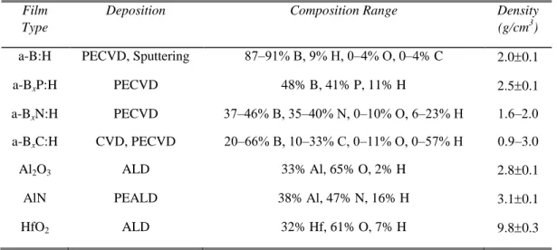
techniques, the details of which are provided elsewhere.21-28 Table I provides a summary of the various films investigated including their nominal composition and deposition method. The thickness of the films utilized in this study ranged from as thin as 100 nm to as thick as several microns. To allow a comparison between the etch rates of the materials described in this study and those from the Si-C-N-O-H composition space, both sets of samples were etched together in the same plasma system as will be described in more detail later.
The composition of all films was determined by combined nuclear reaction analysis (NRA) and Rutherford backscattering (RBS) measurements performed at the University of Albany Dynamitron Accelerator Laboratory. This analysis has been described in detail previously.29 Briefly, the H content was determined using the 15N nuclear reaction method, and the B, C, N and O content was determined using deuteron nuclear reactions. The Al, Si, P, and Hf content was determined by 2 MeV 4He RBS. Given the determined H, B, C, N, O, Al, Si, P, and Hf composition of the films, parameter-free simulations of the full RBS spectra were performed using the program RUMP.29 These RUMP simulations were then compared to the data to provide a powerful
6
check on the analysis. As an additional consistency check, the mass density for all of the films was determined using both NRA-RBS and previously described X-ray reflectivity (XRR) measurements.30 The two techniques were found to typically be in agreement to within 0.1 g/cm3.
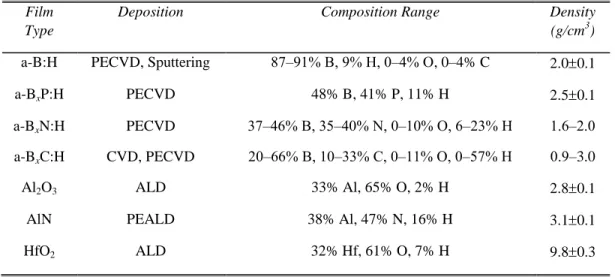
Table I. Summary of properties for high-k and boron dielectrics investigated in this study.
Film Type
Deposition Composition Range Density
(g/cm3)
a-B:H PECVD, Sputtering 87‒91% B, 9% H, 0‒4% O, 0–4% C 2.00.1
a-BxP:H PECVD 48% B, 41% P, 11% H 2.50.1
a-BxN:H PECVD 37‒46% B, 35‒40% N, 0‒10% O, 6‒23% H 1.6‒2.0
a-BxC:H CVD, PECVD 20‒66% B, 10‒33% C, 0‒11% O, 0‒57% H 0.9‒3.0
Al2O3 ALD 33% Al, 65% O, 2% H 2.80.1
AlN PEALD 38% Al, 47% N, 16% H 3.10.1
HfO2 ALD 32% Hf, 61% O, 7% H 9.80.3
To allow for a direct comparison between the dry plasma etch characteristics of the various thin-film materials, they were all etched together in a single plasma etch tool. This was accomplished by cleaving ½ × 1″ coupons of each material from their
respective substrates. These coupons were then loaded onto a handler wafer and etched simultaneously in a 300 mm diameter single wafer Oxford Instruments PlasmaLab Etch 300 RIE system. Portions of each coupon were protected from the plasma etch using a
thin Si beam cleaved from a 300 mm diameter Si (001) wafer and physically placed across each row of coupons (see Figure 1 in Ref. 6). After etching, the etch rate of each
material was determined by either measuring the thickness difference or step height across the exposed and unexposed portions of the coupon. For the former, the thickness of each portion of the coupons was determined using spectroscopic ellipsometry. For the latter, a surface profilometer was used to measure the step height created between the etched and un-etched portions of the sample. The surface profilometer was utilized primarily for samples where the unexposed and exposed portions of the films exhibited low color/thickness contrast that complicated the etch rate measurements using the ellipsometer. In several cases, the exposed portion of the film was completely etched away, thus preventing an accurate measurement of the film etch rate. These results were either excluded from the final analysis or marked as a minimum possible etch rate. In other cases, no transition between the exposed and unexposed portions of the samples could be measured. For these samples, the etch rate was concluded to be zero.
To screen the etch selectivity of the various materials under consideration, the samples were exposed to two different plasma etches typically used for selective SiO2
and a-SiN:H etching. The first plasma etch was a common CHF3 based chemistry used
for selectively etching SiO2 interlayer dielectric (ILD) with a a-SiN:H etch stop (hereafter
designated as the “ILD” etch). The second plasma etch was a common CF4/O2 based
chemistry typically utilized to selectively etch a a-SiN:H etch stop (ES) relative to SiO2
(hereafter designated the “ES” etch). The detailed process conditions used for both the ILD and ES recipes are summarized in our preceeding article.6 We note that while other etch chemistries might be more typically utilized in pitch division patterning processes,
8
the details of these recipes are not typically published in the open literature. In this regard, the CF4/O2 and CHF3 etch chemistries were specifically selected due to both their
complementary selective etching capabilities and the fact that detailed etch process conditions for these chemistries are frequently published in the public domain.
To account for possible run–run and within chamber variability, each dry etch run was repeated three times and typically included 2–3 replicates of each sample placed at opposing positions within the chamber. The three runs were performed using different etch times to accommodate the wide variation in thicknesses and etch rates exhibited by the samples in an attempt to avoid having all of the films of a given type be completely etched through or not etched at all. For additional statistical control, six or more CVD SiO2 samples were also included in each run and randomly distributed within the
chamber. The variability/error for the various thickness or step height measurements was generally <<1 nm and taken to be significantly lower than any sample–sample etch rate variability arising from spatial variations in etch rates within the etch chamber (>1 nm). Additional variability arising from sample–sample composition variability was excluded by utilizing thin film samples with <3% across wafer composition variability and
cleaving replicate samples only from the center of the 300 mm diameter Si (001) wafer. In the results to be presented, we have chosen to plot the results for each individual sample (as opposed to the mean) to more clearly illustrate the number of samples characterized and to highlight any significant sample–sample variability.
III. RESULTS AND DISCUSSION
Due to the large compositional space examined, we begin by first examining the etch behavior for the various high-k dielectrics (Al2O3, AlN, and HfO2). Next, we survey
a series of boron-containing materials (a-B:H, a-BxN:H, a-BxC:H, and a-BxP:H), and
compare their etch behavior to that of representative compounds from the Si-C-O-N-H system (a-C:H, a-Si:H, SiO2, a-Si3N4:H, and a-SiC:H). After establishing general trends,
we examine more subtle effects in the dry etch behavior of the boron-based materials by examining the compositional dependencies within the B-N-H and B-C-H systems. We conclude by comparing the etch behavior of all the different materials and assess whether they might represent potential new and unique etch “colors” for multi-pattern processes.
A. High-k Dielectrics
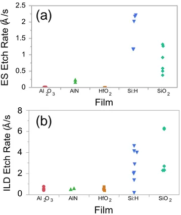
The ES and ILD etch rates for the high-k dielectric materials (Al2O3, AlN, and
HfO2) are summarized in Figure 1. For comparison, results for a-Si:H and SiO2 from a
recent investigation of the Si-C-N-O-H system are also included.6 Each data point represents the results from a single sample. As a reminder, we have chosen to plot the results from each individual sample both to clearly illustrate the number of samples characterized and highlight sample–sample variability arising from variations in the plasma density and uniformity within the plasma etcher. We note that the variability of each individual etch rate measurement for a sample was found to be significantly less than the variability of the sample–sample etch rates arising from variation in spatial etch
10
rates within the plasma etcher. As can be seen, all the high-k dielectrics exhibit zero to negligible etch rates in both the CF4/O2 ES and CHF3 ILD etches.
Å 2 2 3 2 Å 2 2 3 2
(a)
(b)
Figure 1 (Color Online). ES (a) and ILD (b) etch rates for high-k compound dielectrics, a-Si:H, and SiO2. Note: individual data points for a given film have been randomly offset in
some cases to allow greater visibility of all the individual data points.
The low etch rates exhibited by the high-k dielectrics in both fluorinated etches is perhaps not unexpected given the very low volatility for some of the likely etch
by-products such as AlF3 and HfF4.31-33 However, the low etch rates exhibited in both the ES
and ILD etches does indicate that these high-k dielectrics could represent potential third or fourth color materials for certain multi-pass patterning process flows if additional etches capable of etching these high-k materials selective to the Si-based dielectrics can be identified. In this regard, we do note that there is some precedent for this in that high selectivity etching of SiO2 with an AlN hard mask using C4F8 and SF6 chemistries has
been previously reported.34 Additionally, plasma etching of metal oxide hard masks using chlorine-based chemistries,13 and preferential etching of HfO2 optical coatings in a
multilayer stack have also been previously reported.35
B. Boron-Based Dielectrics
To better understand the etch behavior of the various boron-containing
compounds investigated, we first look at the etch rates of low hydrogen content (9%) pure boron films relative to those measured in our previous study6 for pure carbon and silicon films with similar mass density () and hydrogen content. In this regard, Figure 2 summarizes the measured CF4/O2 ES and CHF3 ILD etch rates for the a-B:H ( 2
g/cm3, H = 9%), a-C:H ( = 1.5–2.2 g/cm3, H = 27–33%) and a-Si:H ( 2.3 g/cm3, H = 0–12%) films investigated in this study. For the ES etch (see Fig. 2a), the a-B:H films showed extremely high etch rates ranging from 40–80 Å/s, with some data points actually representing minimum possible etch rates (signified by open markers) due to the films being completely etched through using the times employed to measure reasonable etch rates for the other materials included in the study. In contrast, the a-C:H and a-Si:H films
12
showed negligible to low etch rates ( 1 Å/s). Owing to the similar mass densities and hydrogen contents of these materials, this behavior can be directly attributed to the higher volatility of BF3 and other boron-fluoride etch products likely produced during the
CF4/O2 etching of a-B:H.36 For the ILD etched samples, all the films exhibited similar
etch rates (see Fig. 2b). This can be attributed to the CHF3 etch being a more
polymerizing chemistry37 that co-deposits surface CFx during etching that prevents
greater sub-surface penetration of the plasma activated etch species.38,39
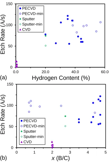
Looking next at multi-element boron-based compounds, Figure 3 summarizes the measured etch rates for non-hydrogenated BxC ( = 2.6–3.0 g/cm3, H 1%, B/C 2)40,
a-BxC:H ( = 1–2 g/cm3, H = 11–55%, B/C = 1–5), a-BxN:H ( 1.7 g/cm3, H 6%,
B/N 1.2), and a-BxP:H ( 2.5 g/cm3, H 11%, B/P 1.2). Alongside the
boron-containing materials in Fig. 3, results from the previous study6 are included for related silicon-based compounds, including a-SiC:H ( 1.7–2.5 g/cm3, H = 32–47%, C/Si = 1) and a-SiN:H ( = 2.6 g/cm3, H = 22%, N/Si=1.35). Focussing first on the CF4/O2 ES etch
rates shown in Fig. 3a, we see that the boron-based dielectrics, as a whole, show substantially higher etch rates relative to the silicon-based materials. In particular, a-BxC:H, and a-BN:H all exhibit etch rates upwards of 80 Å/s. These values are consistent
with prior reports of etch rates of 50 Å/s for CF4/O2 etching of PECVD deposited
a-BN:Hand low carbon content BCN (C 12%) thin films.41,42 The etch rates for these materials along with a-B:H represent a selectivity of almost 100 times relative to important silicon-based dielectrics such as a-Si:H and SiO2, which represents an
improvement of at least double the selectivity of a-SiN:H relative to SiO2, for which the
etch chemistry is specifically optimized.
Å 2 2 3 2 Å 2 2 3 2
(a)
(b)
Figure 2 (Color Online). Etch rates for a-B:H, a-C:H, and a-Si:H thin films in the (a) ES etch and (b) ILD etch. Note: open symbols signify a minimum possible measured etch rate. In some cases, individual data points have been randomly offset to allow greater visibility of all the individual data points.
14
Å
Å
(a)
(b)
Figure 3. ES (a) and ILD (b) etch rates for various boron and silicon dielectric films. See text for range of mass density, hydrogen content, and stoichiometry of the various films. Note: In some cases, individual data points have been randomly offset to allow greater visibility of all the individual data points.
In contrast to the hydrogenated boron compounds, the non-hydrogenated B2C
films exhibit much lower etch rates in the range of 1–15 Å/s, which may be attributed to their significantly higher density (2.6–3.0 g/cm3), and is consistent with the high
chemical inertness and low wet etch rates reported for boron carbide ceramics.43 Finally, the etch rates for the a-BP:H materials are roughly half those for a-BN:H and a-BC:H, although the a-BP:H etch rates remain in the same range as those for the a-SiN:H films. In this case, the reduced a-BP:H etch rates may be attributed either directly to
replacement of carbon or nitrogen by phosphorous and/or the generally lower hydrogen content/higher mass density for the a-BP:H films. Unfortunately, a-BP:H films with greater variation in stoichiometry and hydrogen content were not available for this study.
For the ILD etch, more muted trends were observed with the boron-based films exhibiting, on average, similar but slightly higher etch rates relative to the silicon-based films. Here, the etch rates for high-density B2C and a-BP:H were comparable to those of
a-SiC:H, while those of a-BC:H and a-BN:H were close to those of a-SiN:H. As discussed previously,6 the muted differences between the boron- and silicon-based dielectric films may be attributed to the propensity of the CHF3 ILD chemistry to
co-deposit a CFx polymer layer that makes the etch more physical ion bombardment
driven.37-39 However, the slight differences in ILD etch rates between the boron- and silicon-based compound dielectrics and the variations with the anion constituent suggest that the chemical composition of the material being etched can have a significant
influence on how thick the co-deposited CFx layer grows.
For the boron-based dielectrics, the exceedingly high ES etch rates but comparable ILD etch rates relative to silicon-based dielectrics suggest that these
materials may also represent potential third or fourth color materials. The results in Figs. 2 and 3 clearly demonstrate that these materials can be etched with high selectivity relative to silicon-based materials using a common CF4/O2 based etch. Using the example
16
of dual damascene metal interconnect patterning discussed in a preceeding article,6 the high etch selectivity for the boron-based dielectrics in a CF4/O2 ES breakthrough etch,
but comparable etch rates in a CHF3 ILD pattern transfer etch suggests that they might
naturally serve as an alternative or dual etch stopping layer. For the former, a boron-based dielectric could be utilized to replace a-SiN:H or a-SiCN:H as the etch stop/metal diffusion barrier layer to provide enhanced etch selectivity relative to the ILD material. For the latter, a boron-based dielectric could be used in conjunction with another co-planar etch stop layer and selectively etched through relative to a-SiN:H or a-SiCN:H using a CF4/O2 based chemistry.44 The generally high etch rates for boron-based
dielectrics may also allow their use as hard masking layers where highly polymerizing or non-fluorine-based ILD etches are utilized.24
Due to the compelling etch properties exhibited by some of the boron-based dielectrics, a more detailed examination of the effects of stoichiometry and hydrogen content on boron nitride and boron carbide dielectrics was undertaken. In a previous investigation of silicon-based dielectrics,6 stoichiometry and hydrogen content were found in some cases to have a profound influence on ES and ILD etch rates and offered the possibility for further tuning the etch properties of these materials. As we will show next, similar behavior was observed for a-BxN:H and a-BxC:H materials.
C. B-N-H System
films as a function of both hydrogen content (%) and x (B/N) ratio. No significant correlation was observed between the ES and ILD etch rates and either hydrogen content or B/N ratio. Part of this may be due to the small composition window examined (5–25% hydrogen, B/N = 1.05– .25) as a result of PECVD process limitations in depositing air-stable a-BxN:H films with greater degrees of non-stoichiometry and/or hydrogen
content.45,46 In this regard, we do note that the a-BxN:H ES etch rates shown in Fig. 4b
are comparable to those measured for a-B:H. However, the a-BxN:H ILD etch rates are
roughly five times higher relative to those measured for a-B:H. Thus, fine compositional tuning of a-BxN:H etch rates in CF4/O2 may not be possible while substantial tuning in
CHF3 may be possible by exploring higher B/N ratios than considered here. We also note
that the lack of correlation between ES etch rate and a-BxN:H composition is likely a
result of the thermodynamic instability of BN in the presence of oxygen relative to B2O3,47 and the high volatility for both of the likely etch by-products for a-BxN:H—that
18 0 30 60 90 1 1.1 1.2 1.3 Etch Rate ( Å /s) x (B/N) BN ES BN ILD (b) 0 30 60 90 0 5 10 15 20 25 Etch Rate ( Å /s) Hydrogen Content (%) BN ES BN ILD (a)
Figure 4. ES and ILD etch rates for a-BxN:H as a function of (a) hydrogen content (%)
and (b) B/N ratio, x.
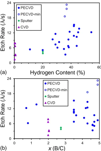
D. B-C-H System
Figures 5 and 6, respectively, summarize the ES and ILD etch rates for a series of CVD, PECVD, and sputter-deposited a-BxC:H films as a function of both hydrogen
content (%) and x (B/C) ratio. Relative to a-BxN:H, a greater variation in dry etch rate
with hydrogen content was observed for a-BxC:H. As shown in Fig. 5a, the a-BxC:H ES
etch rate increases with increasing hydrogen content. However, there is a significant spread in the observed etch rates, which could be due to experimental uncertainties in both the composition and thickness measurements, but could also suggest additional possible effects contributing to the etch rates (vide infra). For the highest hydrogen content films, we note that the data represent minimum possible etch rates due to the films being completely etched through. Extrapolating the trend for the upper band of etch rates to the higher hydrogen contents suggests that etch rates upwards of 150 Å/s may be obtained at hydrogen contents of 55–60%. This suggests that a-BxC:H/SiO2 etch
selectivities as high as 100‒200:1 may be potentially realized, with significant compositional tuning possible as well.
A weak correlation between etch rate and a-BxC:H hydrogen content was also
observed for the ILD etch, where the etch rate remained relatively constant out to 20% and then increased gradually with higher hydrogen content (see Fig. 6a). This may partially explain the lack of an observed correlation between etch rate and hydrogen content for a-BxN:H due to the hydrogen content for those films only approaching 25%
hydrogen. Comparing the ES and ILD a-BxC:H etch rates, the ILD etch rates are
substantially reduced. This is again attributed to the polymerizing nature of the CHF3 ILD
etch chemistry and the formation of a CFx surface layer that impedes plasma etching. In
this regard, we do note that similar etch rates of 2–5 Å/s have been reported for plasma etching of PECVD BCN materials using C4F8 which is another polymerizing etch
20
chemistry.48 As for the ES etch rates, there is also significant scatter in the ILD rates as a function of hydrogen content, with similar possible causes.
0 50 100 150 0.0 20.0 40.0 60.0 Etch Ra te ( Å /s) Hydrogen Content (%) PECVD PECVD-min Sputter Sputter-min CVD (a) 0 50 100 150 0 1 2 3 4 5 Etch Ra te ( Å /s) x (B/C) PECVD PECVD-min Sputter Sputter-min CVD (b)
Figure 5. ES etch rates for a-BxC:H as a function of (a) hydrogen content (%) and (b) B/C
0 6 12 18 24 0 20 40 60 Etch Ra te ( Å /s) Hydrogen Content (%) PECVD PECVD-min Sputter CVD (a) 0 6 12 18 24 0 1 2 3 4 5 Etch Ra te ( Å /s) x (B/C) PECVD PECVD-min Sputter CVD (b)
Figure 6. ILD etch rates for a-BxC:H as a function of (a) hydrogen content (%) and (b)
B/C ratio, x.
To examine the influence of B/C stoichiometry, the a-BxC:H ES and ILD etch
rates were plotted as a function of B/C ratio, as shown in Figs. 5b and 6b, respectively. Taken as a whole, no clear correlation between either ES or ILD etch rate and B/C ratio was observed. For ES etch rate, Fig. 5b does appear to show a local minimum at a B/C ratio of 2 suggesting that this is perhaps a unique or singular stoichiometry from an etch
22
perspective. However, we note that the a-BxC:H films with x = 2 were deposited by high
temperature CVD and have a very low hydrogen content relative to the rest of the films which were primarily deposited by lower temperature PECVD methods. The chemical bonding/molecular structure of the CVD and PECVD a-BxC:H films are accordingly
substantially different. For the former, carbon is present primarily in tetrahedral BC4 and
trigonal BC3 intericosahedral sites, intraicosahedral sites, with some free/excess carbon
also a possibility.49 For the latter, a substantial amount of carbon has been shown to also exist as extraicosahedral hydrocarbon species in addition to occupying intraicosahedral sites within C2B10 icosahedra.50 The lack of correlation between etch rate and B/C ratio,
and weak correlation with hydrogen concentration, could be due to more subtle effects such as how carbon is specifically incorporated into the film and/or the presence of nano-porosity as was previously observed for a-SiOC:H materials.6 However, without knowing the detailed microstructure of these materials, it is evidently difficult to tease out clear trends from simple correlation plots. From the data presented, it thus appears that in the a-BxC:H films, the B/C ratio can be tuned continuously from < 1 to 5 with relatively little
variation in ES or ILD etch rate as shown in Fig. 5b.
To further explore the possibility of a more complex relationship between etch rate and stoichiometry, a statistical response surface (RS) analysis was performed for both the a-BxC:H ES and ILD etch ratesusing Jmp 11.0 statistical analysis software
(SAS).51 The mixture RS analysis specifically used standard least squares and effects screening methods to fit the response (ES or ILD etch rate) to a polynomial that included
both linear and two factor elemental composition interaction terms. The resulting coefficient of determination (R2) from the statistical analysis was used to judge the quality of fit to the polynomial model where R2 close to 1 indicates an excellent fit and R2 approaching 0 indicates a poor or lack of fit. To look for subtle effects that might be masked by examining a limited composition range within the a-BxC:H system, the results
for a-B:H presented in the preceeding section and a-C:H results presented in a preceeding article6 were also included. This allowed the B-C-H composition space to be more fully examined. To allow a robust analysis, all minimum etch rate data points shown in Figs. 2-6 were excluded.
The results of the response surface analysis for both the ES and ILD etches are presented as ternary etch rate diagrams in Figure 7. Each side of the triangle represents the axis for one of the three elemental components of the system (i.e., % B, C, and H) with the three corners signifying a composition of 100% for each element. The illustrated data points are plotted such that each elemental concentration decreases in proportion to the distance from the corner of the triangle representing that element. The color shading illustrates the ES and ILD etch rates predicted by the RS model as a function of
composition. The solid circle data points in each ternary plot signifies the composition for the individual films utilized in the response surface modeling while open circles signify compositions where only minimum possible etch rates could be determined (but were not included in the actual response surface modeling). The triangle of open diamond data points in the right corner marks the region defined by constraint theory where
24 Å Å
(b)
(a)
Figure 7. Ternary response surface model for the B-C-H system for (a) ES etch rates, and (b) ILD etch rates. Note: Solid circles indicate data points used in response surface model and open circles represent compositions where minimum etch rates were determined but not included in the model. Open triangles signify compositions where continuously networked films are not expected based on topological constraint theory.
indicating that a reasonable fit to the experimental data was obtained and that 85% of the observed variability in etch rate was captured. As shown in Fig. 7a, the RS model
predicts a maximum ES etch rate on the B-H tieline at approximately 70% B and 30% H. This maximum decreases along a ridge that decreases and intersects the C-H tieline at approximately 70% C and 30% H. Overall, the RS model captures the observed high and low etch rates for a-B:H and a-C:H, respectively, and also indicates a general decrease in etch rate with decreasing hydrogen content and increasing carbon content. The model further suggests that the influence of increasing hydrogen content diminishes on increasing ES etch rate as carbon content increases. Unfortunately, this portion of the model is not experimentally validated due to all the films in this composition regime being completely etched through and excluded from the analysis. Thus, extrapolation of the RS model outside the experimentally sampled composition space should be done so with some caution.
For the a-BxC:H ILD etch rate, an R2 value of 0.72 was obtained, indicating that
the RS model fitted only 72% of the observed variability in etch rate. As shown in Fig. 7b, the a-BxC:H ILD etch RS model again predicts a maximum in etch rate at hydrogen
rich conditions. In this case, however, the predicted maximum etch rate decreases more gradually with decreasing hydrogen/increasing carbon-boron content relative to the ES etch. The reduced sensitivity to carbon content is likely due to the previously mentioned highly polymerizing nature and propensity of the CHF3 ILD etch to co-deposit a CFx
surface layer during etching. The presence of co-deposited carbon thus mitigates to some extent the presence of carbon in the a-BxC:H film. In this regard, we note that a similar
26
effect was also observed for the a-SiCx:H system where the influence of carbon content
on etch rates was also more muted in the CHF3 ILD etch.6
Concerning the viability of a-BxC:H as a potential third or fourth color dielectric,
Figs. 5–7 clearly illustrate that significant order of magnitude tuning of the etch characteristics of this material in a fluorinated plasma etch chemistry is possible via optimization of the films elemental composition and detailed chemical / molecular structure. This is important both from an etch perspective as well as providing lattitude for co-optimization of other material characteristics that may also be of importance such as thermodynamic stability and thermal, mechanical, electrical, and optical properties. In this regard, a-BxC:H is highly attractive due to recent demonstrations of the ability to
significantly tune the excellent electrical, optical, thermal, and mechanical properties exhibited by this material.21-23 The potential capacity to co-optimize both etch and salient material properties with a-BxC:H, therefore, makes it of extreme interest as a potential
third or fourth color material in low-k etch stop, diffusion barrier, hard mask, or spacer applications for pitch division / multi-pattern processing. However, significantly more characterization of the dry etch properties of a-BxC:H materials in other halogenated
chemistries commonly used in multi-pass patterning methods (i.e. Cl2, Br2, SF6, ...) will
be needed to further assess their viability.
Two fluorinated plasma etches commonly utilized to selectively etch SiO2 ILD
(CHF3) and a-SiN:H ES (CF4/O2) materials were utilized to survey the etch
characteristics of various high-k dielectric (Al2O3, AlN, HfO2) and boron-containing
materials (a-B:H, a-BxN:H, a-BxP:H, a-BxC:H) relative to those from within the
Si-C-O-N-H system to identify possible third or fourth color multi-pattern etch stop materials. The high-k dielectrics all exhibited very low to unmeasureable etch rates in both etches suggesting their potential as possible third/fourth color dielectric materials provided etch chemistries capable of selectively etching these materials relative to other silicon- and carbon-based materials can be identified. In contrast, the boron-based dielectrics all exhibited order of magnitude or higher etch rates in the CF4/O2 ES etch relative to
silicon-based materials while still exhibiting comparable etch rates in the CHF3 ILD etch.
A more detailed examination of the B-C-H system suggests that optimization of etch selectivity for a-BxC:H can be achieved via compositional tuning, although the
relationship between etch rate and microstructure may be complex as in the
a-SiOC:H/SiCO:H system.6 Most importantly, recent demonstrations21-23 of the ability to significantly tune the excellent electrical, optical, thermal, and mechanical properties of a-BxC:H suggest the potential capacity to co-optimize both etch and salient material
properties. This strongly suggests the viability of a-BxC:H and related materials as
potential third or fourth color etch stop, diffusion barrier, hard mask, or spacer materials in pitch division / multi-pattern processing.
28
The authors would like to acknowledge Drs. Tim Glassman, and Andre Baran of Intel Corporation for their assistance in providing some of the high-k dielectric materials examined in this study. The authors would also like to acknowledge Joe Sandstrom at the Center for Nanoscale Science and Engineering at North Dakota State University for preparing several of the boron-based materials investigated in this study. UMKC
acknowledges financial support from Intel Corporation (contract no. 2012-IN-2313) and the Defense Threat Reduction Agency (grant no. HDTRA1-15-1-0020).
1
C. Mack, J. Micro/Nanolith. MEMS MOEMS 12, 030101 (2013).
2
H. Hody, V. Paraschiv, D. Hellin, T. Vandeweyer, G. Boccardi, and K. Xu, J. Micro/Nanolith. MEMS MOEMS 14, 014504 (2015).
3
J. Chawla, K. Singh, A. Myers, D. Michalak, R. Schenker, C. Jezewski, B. Krist, F. Gstrein, T. Indukuri, and H. Yoo, Proc. of SPIE 9054, 905404 (2014).
4Martin Gardner, “The Four Color Map Theorem” in Sphere Packing, Lewis Carroll, and Reversi
(Cambridge University Press, New York, 2009).
5
S. King, ECS J. Solid State Sci. Technol. 4, N3029 (2015).
6
S. Dhungana, T. Nguyen, B. Nordell, M. Paquette, A. Caruso, W. Lanford, K. Scharfenberger, D. Jacob, and S. King, submitted to J. Vac. Sci. Technol.
7
S. Pauliac-Vaujour, P. Brianceau, C. Comboroure, and O. Faynot, J. Vac. Sci. Technol. B 31, 021603 (2013).
8
C. Ho, X. Lin, H. Chien, and C. Lien, Thin Solid Films 518, 6076 (2010).
9
10
H. Hody, V. Paraschiv, E. Vecchio, S. Locorotondo, G. Winroth, R. Athimulam, and W. Boullart, J. Micro-Nanolith. MEMS MOEMS 12, 041306 (2013).
11
G. Wilk, R. Wallace, and J. Anthony, J. Appl. Phys. 89, 5243 (2001).
12
J. Robertson, Rep. Prog. Phys. 69, 327 (2006).
13
J.-F. de Marneffe, L. Zhang, M. Heyne, M. Lukaszewicz, S.B. Porter, F. Vajda, V. Rutigliani, Z. el Otell, M. Krishtab, A. Goodyear, M. Cooke, P. Verdonck, and M. Baklanov, J. Appl. Phys. 118, 133302 (2015).
14
S. Nguyen, T. Nguyen, H. Treichel, and O Spindler, J. Electrochem. Soc. 141, 1633 (1994).
15
W. Kane, S. Cohen, J. Hummel, B. Luther, and D. Beach, J. Electrochem. Soc. 144, 658
16
B. Neureither, C. Basa, T. Sandwick, and K. Blumenstock, J. Electrochem. Soc. 140, 3607 (1993).
17
T. Sugino, Y. Etou, T. Tai, and H. Mori, Appl. Phys. Lett. 80, 649 (2002). (1997).
18
Y. Kumashiro, J. Mater. Res. 5, 2933 (1990).
19
D. Music, V. Kugler, Z. Czigany, A. Flink, O. Werner, J. Schneider, L. Hultman, and U. Helmersson, J. Vac. Sci. Technol. A 21, 1355 (2003).
20
V. Mohammadi, W. de Boer, T. Scholtes, and L. Nanver, ECS J. Solid State Sci. Technol. 1, Q16 (2012).
21
B. Nordell, S. Karki, T. Nguyen, P. Rulis, A. Caruso, S. Purohit, H. Li, S. King, D. Dutta, D. Gidley, W. Lanford, and M. Paquette, J. Appl. Phys. 118, 035703 (2015).
22
B. Nordell, C. Keck, T. Nguyen, A. Caruso, S. Purohit, W. Lanford, D. Dutta, D. Gidley, P. Henry, S. King, and M. Paquette, Mat. Chem. Phys. 173, 268 (2016).
23
B.J. Nordell, T. Nguyen, C. Keck, S. Dhungana, A. Caruso, W. Lanford, J. Gaskins, P. Hopkins, D. Merrill, D. Johnson, L. Ross, P. Henry, S. King, and M. Paquette, Adv. Elect. Mater. 2, 1600073 (2016).
30
24
L. Xia, D. Cui, M. Balseanu, V. Nguyen, K. Zhou, J. Pender, and M. Naik, ECS Trans. 35, 651 (2011).
25
S. King, M. French, M. Jaehnig, M. Kuhn, and G. Xu, ECS J. Solid State. Sci. Technol. 1, P250 (2012).
26
S. King, M. Paquette, J. Otto, A. Caruso, J. Brockman, J. Bielefeld, M. French, M. Kuhn, and B. French, Appl. Phys. Lett. 104, 102901 (2014).
27
N. Alimardani, S. King, B. French, C. Tan, B. Lampert, and J. Conley, Jr., J. Appl. Phys. 116, 0234508 (2014).
28
B. French and S. King, J. Mater. Res. 28, 2771 (2013).
29
W. Lanford, M. Parenti, B. Nordell, M. Paquette, A. Caruso, M. Mantymaki, J. Hamalainen, M. Ritala, K. Klepper, V. Miikkulainen, O. Nilsen, W. Tenhaeff, N. Dudney, D. Koh, S. Banerjee, E. Mays, J. Bielefeld, and S. King, Nuc. Instr. Methods Phys. Res. B 371, 211 (2016).
30
S. King, J. Bielefeld, G. Xu, W. Lanford, Y. Matusda, R. Dauskardt, N. Kim, D. Hondongwa, L. Olasov, B. Daly, G. Stan, M. Liu, D. Dutta, and D. Gidley, J. Non-Cryst. Sol. 379, 67 (2013).
31
M. Watanabe, T. Iida, K. Akiyama, S. Narita, T. Ishikawa, H. Sakai, K. Sawabe, and K. Shobatake, Jpn. J. Appl. Phys., Part 2 42, L356 (2003).
32
M. Watanabe, Y. Mori, T. Ishikawa, H. Sakai, T. Iida, K. Akiyama, S. Narita, K. Sawabe, and K. Shobatake, J. Vac. Sci. Technol. A 23, 1647 (2005).
33
S. King, R. Davis, and R. Nemanich, J. Vac. Sci. Technol. A 32, 051402 (2014).
34
K. Kolari, Microelectron. Eng. 85, 985 (2008).
35
T. Alig, S. Gunster, and D. Ristau, Thin Solid Films 592, 237 (2015).
36
37
V. Donnelly and A. Kornblit, J. Vac. Sci. Technol. A 31, 050825 (2013).
38
T. Standaert, E. Joseph, G. Oehrlein, A. Jain, W. Gill, P. Wayner, and J. Plawsky, J. Vac. Sci. Technol. A 18, 2742 (2000).
39
A. Sankaran and M. Kushner, Appl. Phys. Lett. 82, 1824 (2003).
40
J. Berjonneau, G. Chollon and F. Langlais, J. Electrochem. Soc. 153 C795 (2006).
41
D. Cote, S. Nguyen, D. Dobuzinsky, C. Basa, and B. Neureither, J. Electrochem. Soc. 141, 2456 (1994).
42
H. Aoki, S. Tokuyama, T. Sasada, D. Watanabe, M. Mazumder, C. Kimura, and T. Sugino, Diam. Rel. Mater. 17, 1800 (2008).
43
F. Thevenot, J. Eur. Ceram. Soc. 6, 205 (1990).
44
C. Carver, J. Plombon, P. Romero, S. Suri, T. Tronic, and R. Turkot, Jr., ECS J. Solid State Sci. Technol. 4, N5005 (2015).
45
J. Andujar, E. Bertran, and M. Polo, J. Vac. Sci. Technol. A 16, 578 (1998).
46
A. Soltani, P. Thevenin, H. Bakhtiar, and A. Bath, Thin Solid Films 471, 277 (2005).
47
R. Paine and C. Narula, Chem. Rev. 90, 73 (1990).
48
H. Aoki, M. Hara, T. Masuzumi, F. Ahmed, C. Kimura, and T. Sugino, Diam. Relat. Mater 19, 507 (2010).
49
C. Pallier, J. Leyssale, L. Truflandier, A. Bui, P. Weisbecker, C. Gervais, H. Fischer, F. Sirotti, F. Teyssandier, and G. Chollon, Chem. Mater. 25, 2618 (2013).
50
M. Paquette, W. Li, M. Driver, S. Karki, A. Caruso, and N. Oyler, J. Phys.: Condens. Matter 23, 435002 (2011).
51
SAS, Cary NC 27513 USA.
52
J. Phillips and M. Thorpe, Sol. Stat. Comm. 53, 699 (1985).
53
32
Table I. Summary of properties for high-k and boron dielectrics investigated in this study.
Film Type
Deposition Composition Range Density
(g/cm3)
a-B:H PECVD, Sputtering 87‒91% B, 9% H, 0‒4% O, 0–4% C 2.00.1
a-BxP:H PECVD 48% B, 41% P, 11% H 2.50.1
a-BxN:H PECVD 37‒46% B, 35‒40% N, 0‒10% O, 6‒23% H 1.6‒2.0
a-BxC:H CVD, PECVD 20‒66% B, 10‒33% C, 0‒11% O, 0‒57% H 0.9‒3.0
Al2O3 ALD 33% Al, 65% O, 2% H 2.80.1
AlN PEALD 38% Al, 47% N, 16% H 3.10.1
Figure Captions
Figure 1 (Color Online). ES (a) and ILD (b) etch rates for high-k compound dielectrics, a-Si:H, and SiO2. Note: individual data points for a given film have been randomly offset in
some cases to allow greater visibility of all the individual data points.
Figure 2 (Color Online). Etch rates for a-B:H, a-C:H, and a-Si:H thin films in the (a) ES etch and (b) ILD etch. Note: open symbols signify a minimum possible measured etch rate. In some cases, individual data points have been randomly offset to allow greater visibility of all the individual data points.
Figure 3 (Color Online). ES (a) and ILD (b) etch rates for various boron and silicon dielectric films. See text for range of mass density, hydrogen content, and stoichiometry of the various films. Note: In some cases, individual data points have been randomly offset to allow greater visibility of all the individual data points.
Figure 4 (Color Online). ES and ILD etch rates for a-BxN:H as a function of (a) hydrogen
content (%) and (b) B/N ratio, x.
Figure 5 (Color Online). ES etch rates for a-BxC:H as a function of (a) hydrogen content
34
Figure 6 (Color Online). ILD etch rates for a-BxC:H as a function of (a) hydrogen content
(%) and (b) B/C ratio, x.
Figure 7 (Color Online). Ternary response surface model for the B-C-H system for (a) ES etch rates, and (b) ILD etch rates. Note: Solid circles indicate data points used in response surface model and open circles represent compositions where minimum etch rates were determined but not included in the model. Open triangles signify compositions where continuously networked films are not expected based on topological constraint theory.