HAL Id: hal-01794379
https://hal.archives-ouvertes.fr/hal-01794379
Submitted on 15 Jun 2018
HAL is a multi-disciplinary open access
archive for the deposit and dissemination of
sci-entific research documents, whether they are
pub-lished or not. The documents may come from
teaching and research institutions in France or
abroad, or from public or private research centers.
L’archive ouverte pluridisciplinaire HAL, est
destinée au dépôt et à la diffusion de documents
scientifiques de niveau recherche, publiés ou non,
émanant des établissements d’enseignement et de
recherche français ou étrangers, des laboratoires
publics ou privés.
Local Schottky contacts of embedded Ag nanoparticles
in Al 2 O 3 /SiN x :H stacks on Si: a design to enhance
field effect passivation of Si junctions
E Elmi, R Cristini-Robbe, M. Chen, B Wei, R. Bernard, Dmitri Yarekha, E
Okada, Saliha Ouendi, X. Portier, F. Gourbilleau, et al.
To cite this version:
E Elmi, R Cristini-Robbe, M. Chen, B Wei, R. Bernard, et al.. Local Schottky contacts of embedded
Ag nanoparticles in Al 2 O 3 /SiN x :H stacks on Si: a design to enhance field effect passivation
of Si junctions. Nanotechnology, Institute of Physics, 2018, 29 (28), �10.1088/1361-6528/aac032�.
�hal-01794379�
Local Schottky contacts of embedded Ag
nanoparticles in Al
2
O
3
/SiN
x
:H stacks on Si: a
design to enhance
field effect passivation of
Si junctions
O Ibrahim Elmi
1, O Cristini-Robbe
2, M Y Chen
3, B Wei
3, R Bernard
2,
D Yarekha
4, E Okada
4, S Ouendi
4, X Portier
5, F Gourbilleau
5, T Xu
3,6and
D Stiévenard
4,61
Université de Djibouti, Faculté des Sciences BP 1904, Djibouti
2PHLAM, UMR8523, Université de Lille 1, F-59652 Villeneuve d’Asq Cédex, France 3
Key Laboratory of Advanced Display and System Application, Shanghai University, 200072 Shanghai, People’s Republic of China
4IEMN, UMR8520, Université de Lille1, F-59652 Villeneuve d’Ascq Cédex, France 5
CIMAP, Normandie Univ, ENSICAEN, UNICAEN, CEA, CNRS, 6 Boulevard Maréchal Juin, F-14050 Caen Cedex 4, France
E-mail:xtld@shu.edu.cnanddidier.stievenard@iemn.univ-lille1.fr
Abstract
This paper describes an original design leading to thefield effect passivation of Si n+-p junctions. Ordered Ag nanoparticle(Ag-NP) arrays with optimal size and coverage fabricated by means of nanosphere lithography and thermal evaporation, were embedded in
ultrathin-Al2O3/SiNx:H stacks on the top of implanted Si n+-p junctions, to achieve effective
surface passivation. One way to characterize surface passivation is to use photocurrent, sensitive to recombination centers. We evidenced an improvement of photocurrent by a factor of 5 with the presence of Ag NPs. Finite-difference time-domain(FDTD) simulations combining with semi-quantitative calculations demonstrated that such gain was mainly due to the enhancedfield effect passivation through the depleted region associated with the Ag-NPs/Si Schottky contacts. Keywords:field effect passivation, silver nanoparticles, Al2O3/SiNxstacks, FDTD simulation
1. Introduction
Recombination process in n-p (or p-n) junction mainly through defects [1] is a bottleneck to overcome in order to
improve the efficiency of light absorption and its conversion into photocurrent, with solar cells as one main application. First, a variety of approaches has been applied to increase light absorption, such as surface texturing and light frequency conversion[2–4]. In particular, research for light trapping has
focused on the surface plasmons technology via metallic
nanoparticles(NPs) over the past decades [5,6]. It has been
established that surface plasmons induced by light illumina-tion on noble metallic NPs result in scattering or absorpillumina-tion of light[7,8]. Furthermore, light trapping can be optimized by
engineering the size, shape and density of NPs [9–12]. This
area of research is still very active and many questions remained open[13]. As a result, there is a need to improve the
fabrication process of NP arrays to achieve optimized cov-erage. One approach is to use the nanosphere lithography (NSL) that is known to be a low-cost and high-efficiency fabrication technique for the creation of NP arrays with a controlled size and coverage rate [14]. Recently, Gao et al 6
have demonstrated that this method has large area capability and compatibility with various types of substrates, which could be further applied in the industry[15].
Once light absorption is optimized, it is also important to improve the surface passivation[16]. In general, metallic
NPs could be embedded in a passivation layer to hinder the formation of metallic NP recombination centers and to prevent the oxidation of metal [17]. It was found that the
Al2O3 films deposited by atomic layer deposition (ALD)
demonstrated excellent passivation effect comparing with the widely used passivation layers such as thermally grown SiO2 [18] and plasma-enhanced chemical vapor deposited
(PECVD) SiNx:H [19], taking advantage of the unique
features of precise growth control, high uniformity and excellent conformity of ALD deposition [20]. Al2O3 films
combine a high level of chemical passivation with an effective field-effect passivation, which is generated by a high density of negativefixed charges in the Al2O3[21,22].
Some earlier works showed that thefield-effect passivation remained high down to an Al2O3thickness of 2 nm, while
the chemical passivation was deteriorated[23]. In that case,
effective chemical passivation can be achieved by the dif-fusion of hydrogen from an additional SiNx:H layer to the Si
interface. As a result, stacks of an ultrathin Al2O3tunneling
layer(1–2 nm) in combination with a capping layer such as SiNx:H have showed promising passivation results for both
p and n-type Si cells[24–28]. It is thus necessary to get a
deeper insight into thefield-effect passivation effect of such configuration, as well as the plasmonic effect associated with the metallic NPs.
In this work, we showed that, by combining Ag-NPs with the Al2O3/SiNx:H stacks on implanted Si n+-p junctions, it is
possible to dramatically reinforce thefield-effect passivation through the local depleted space region associated with the Ag-NPs/Si local Schottky contacts, which is confirmed by photocurrent measurements. Ag-NP arrays with optimal size and coverage rate were fabricated by using NSL method while their optical properties have been investigated. Ag is the material of choice because of its low parasitic light absorption and good scattering properties [29]. It is worth noting that,
neglecting the promising issue of plasmonic structures and passivation formed on the rear-side of Si junctions[30], we
focus on the passivation effect of front-side in this work. Furthermore, finite-difference time-domain (FDTD) simula-tions were used to compare and explain the experimental results.
2. Methods
2.1. Device fabrication
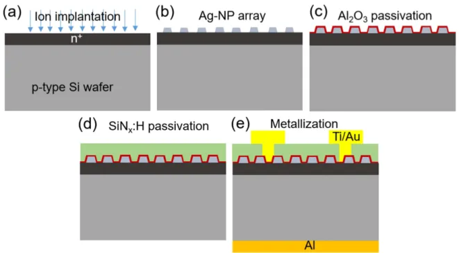
Figure 1 shows the fabrication process of Ag-NPs based implanted Si n+-p junctions with surface passivation of Al2O3/SiNx:H stacks. Four-inch boron-doped p-type silicon
(100) wafers with a resistivity of 5–10 Ω cm were used as substrate. The samples were cleaned using piranha solution
and distilled water before the realization of n+ top layer. Phosphorous ions implantation was performed using a dose of 1014at cm–2at 180 KeV, followed by an annealing at 900°C during 5 min to activate the dopants. A detailed description of the implantation process is described in our previous work [31].
Two-dimensional ordered Ag-NP arrays were deposited by combining NSL technique and thermal evaporation. Monodisperse SiO2nanospheres with different diameters D
(D=2r) ranging from 230 to 400 nm were purchased from Gmbh microparticles, and assembled into a close packed monolayer on Si wafer using Langmuir Blodgett(LB) tech-nique, acting as the mask. The size and spacing of the NPs were controlled by isotropic reactive ion etching (RIE) of SiO2using a mixture of CHF3and O2with power of 100 W
and pressure of 250 mTorr. Thermal evaporations of Ag were then performed on SiO2 nanospheres to deposit Ag layers
with different thicknesses ranging from 40 to 60 nm, while the substrate was kept at room temperature during evapora-tion. The SiO2 nanospheres were then removed by using
ultrasonic in isopropanol, giving an ordered array of Ag-NPs with triangular shape on the substrate.
First, an ultrathin Al2O3tunneling layer with a thickness
of 1.5 nm was deposited on the Ag-NP array by using ALD technique. The deposition was carried out in a TFS200 Beneq system with a thermal process. The reactants used were tri-methylaluminum (TMA) and H2O, while the growth
temp-erature was 290°C. Second, a SiNx:H layer with a thickness
of 80 nm which corresponds to the value usually used in Si-solar cell industry, was deposited on the sample by using PECVD with a mixture of SiH4 and NH3. The deposition
temperature was 340°C, while the pressure was 1 Torr and the power was 10 W. Sample was then annealed at 500°C for 30 min to make H diffusing into Si. In addition, a sample with only SiNx:H passivation layer was fabricated as control
device.
Finger electrodes of Ti/Au (20/800 nm) were deposited on the front-side by sputtering with a shadow mask after the opening of the SiNx:H coating by using RIE etching. The
back contact was then deposited by evaporating Alfilms of 400 nm. Finally, the samples were annealed at 400°C for 10 min to form Ohmic contact.
2.2. Characterization
The Ag-NP arrays were characterized by scanning electron microscopy (SEM, ZEISS ultra 55) to determine their size, spatial distribution and also surface coverage. The reflectance was measured using an UV–vis spectrophotometer (VARIAN CARY 5000), equipped with an integrating sphere (DRA-2500 LABSPHERE). The photoconductivity measurements were done using a monochromatic source (ORIEL) with a 200 W Tungsten light, allowing a spectroscopic analysis from 300 to 1200 nm. The photon flux was calibrated using a thermopile detector with a broad flat spectral response from 200 nm to 50 microns. All the photocurrent curves were therefore normalized and thus independent of the intensity of
the source. In order to increase the signal/noise ratio, the light flux was chopped at a frequency of 2.5 Hz and a lock-in detection was used.
The TEM analysis was done from cross sectional thin foils prepared by a focused ion beam (FIB) system. Prior to the ion thinning down, a carbon film and a platinum layer were deposited to protect the top surface of the sample. The TEM and HREM observations were done with a JEOL 2010 microscope operated at 200 kV and equipped with an energy dispersive x-ray(EDX) spectrometer (EDAX setup). The image processing
was performed using DIGITALMICROGRAPH (GATAN).
The images were taken with the electron beam parallel to the [011] direction of the Si (100) oriented substrate. In this orien-tation, the electron beam is parallel to the Ag particles/substrate interface.
2.3. FDTD simulations
FDTD simulations were performed using a commercially available package from OptiwaveTM to simulate the optical absorption of the samples. The OptiFDTD software is based on the FDTD algorithm proposed by K S Yee en (1966) [32], which introduced a modeling technique with second
order central differences to solve the Maxwell equations applying afinite-difference approach. The FDTD algorithm can directly calculate the value of E(electric field intensity) and H (magnetic field intensity) at different points of the computational domain. The excitation field is a Gaussian modulated continuous wave with the center wavelength of 550 nm.
3. Results and discussion
Figure2(a) shows a close packed monolayer of monodisperse
SiO2 nanospheres with diameter D (D=2r) of 400 nm,
assembled on Si substrate by using LB technique. The size and spacing of the NPs were further tuned by using isotropic RIE of SiO2[33,34]. Ag films were then deposited on SiO2
nanospheres as shown in figure2(b). Figure 2(c) displays a
top-view SEM image of the Ag deposition in one particular area. It can be observed that Ag filled well the voids of the nanosphere monolayer in a triangular shape. The honeycomb ordered array of Ag-NPs wasfinally obtained after removing the SiO2nanospheres, as it is shown infigure2(d). The height
of Ag-NPs depends on the evaporation thickness of Ag, which is well controlled in all samples.
NSL technique leads to an easy and precise control of the density of the NPs as well as their height, which is a great advantage compared with the dewetting of a thin metallic layer. In such a case, the density and the height of the NPs depend on the time, the temperature and the quantity of deposited metal, as well as the atomic structure of the surface, this last point being more difficult to control. Moreover, it is interesting to note that the following concept is independent of the metal used(in the limit of technological compatibility) and therefore is quite general.
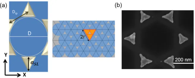
Ag-NP array was modeled in FDTD simulations by con-sidering the unit cell as shown in figure 3(a), and by
imple-menting periodic boundary conditions in the array(x, y) plane. The relevant geometric parameters were the distance Dip
between the centers of two neighboring NPs, the thickness h and the size aSLof each NP. The NPs were placed directly on
Figure 1.Schematic of fabrication process of Ag-NPs based implanted Si n+-p junction.(a) Formation of n+top layer on p-type Si wafer, (b) Ag-NP arrays deposited by NSL technique and thermal evaporation, (c) deposition of Al2O3tunneling layer by ALD,(d) deposition of
the substrate and the interface between the substrate and the medium was at the z=0 plane. Over the NPs, the medium (air) was considered as semi-infinite. When necessary, Al2O3
and SiNx:H layers were added. The semi-infinite conditions
were necessary to hinder radiation back-scattering from the external. This was done by using perfectly matched layer sub-domains.
To obtain good light absorption of Ag-NP arrays and to avoid large shading effect, it is of great importance to opt-imize the surface coverage of the arrays which is reported to
be around 10%[12]. The theoretical surface coverage (Sc) of
Ag-NPs fabricated by NSL technique can be easily calculated from the geometrical parameters of the array shown in figure 3(a). It is found that Sc does not depend on the
dia-meter of SiO2nanospheres with a constant value of 9% close
to the optimum value.
= = - = p -( ) / SC r r 3 3 0.09 1 A A A r triangle 3 circle 6 triangle 2 2 2 2
Figure 2.SEM images of(a) SiO2nanosphere monolayer.(b) SiO2nanospheres coated by Agfilm after thermal evaporation. (c) Top-view
SEM image of Ag deposition.(d) Ag-NP array after the removing of the SiO2nanospheres.
Figure 3.(a) Scheme for the FDTD simulation of the unit cell with the geometrical parameters of a metallic NP and an overview of the NP array.(b) SEM image of a part of Ag-NP array obtained from SiO2nanospheres with diameter D of 400 nm.
SEM observations coupled with MountainsMapTM soft-ware analysis were used to estimate the experimental surface coverage of Ag-NPs, which was measured to be around 10%, slightly higher than the theoretical value. The slight increase of experimental value can be explained by the non-perfect compactness of the SiO2nanosphere monolayer. An example
of Ag-NP array obtained from SiO2 nanospheres with
dia-meter of 400 nm is shown infigure3(b). The calculated grain
surface coverage is 10.7%.
The optical properties of Ag-NP array with different densities(different nanosphere diameters) and Ag thicknesses were studied. It should be noted that the Ag thickness was kept less than that of the SiNxlayer(80 nm) to ensure a good
coverage of the passivation layer on Ag-NP arrays. Figure4
shows the evolution of the reflectance spectra as a function of Ag thicknesses (40 and 60 nm) and nanosphere diameters (230, 300 and 400 nm).
The reflectance globally decreased when the density of Ag-NPs increased, in other words, when the diameter of SiO2
nanospheres used to fabricate Ag-NPs decreased from 400 to
230 nm. The same trend was observed when the thickness of Ag-NPs was increased from 40 to 60 nm. As a result, the best Ag-NP array giving the minimum of reflectance with an average value of ∼42% (lower than that of the Si reference ∼53%), was obtained with a high Ag-NPs density (fabricated from the smallest SiO2nanospheres 230 nm) and a thick Ag
layer (60 nm). Such configuration was then applied in the following devices.
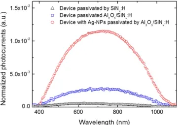
Passivation effect based on Al2O3/SiNx:H stacks
depos-ited by means of ALD and PECVD techniques, including or not Ag NPs were studied by means of photoconductivity measurements. Figure 5 gives the associated photocurrent measurements.
The control device passivated by SiNx:H layer showed a
very weak photocurrent. Indeed, during the fabrication of the metallic contacts on the devices, the etching of SiNx:H layer
led to locally damaged and unpassivated contact surface which resulted in important serial resistance (greater than a few ohm cm2) with subsequent degradation of the electrical per-formances. The insertion of an Al2O3tunneling layer became
thus necessary, which is known to be a good passivation candidate for metallic contacts without affecting their ohmic nature [35]. Furthermore, the Al2O3 tunneling layer can be
used not only as passivation layer but also as a control of the SiNxetching to avoid any degradation of the Si substrate,
since Al2O3is known to be hardly etched by RIE process. Such
stack structure allows both good chemical and field effect passivation. The junction passivated by stacks of Al2O3
(1.5 nm) and SiNx:H (80 nm) exhibited an increasing of the
photocurrent by a factor of 4 compared to that of the control device. In addition to the passivation effect, the embedded Ag-NPs in the Al2O3/SiNx:H stacks gave a gain of 5 on the
photocurrent compared with the Al2O3/SiNx:H-passivated
device without Ag-NPs. In total, the use of Ag-NPs combining with the Al2O3/SiNx:H stack passivation resulted in a typical
gain of around 20 on photoconductivity comparing with the control device.
FDTD simulations of the optical absorption versus the different passivation process were performed to get a better
Figure 4.Reflectance of Ag-NP arrays for different Ag thicknesses (40 and 60 nm) and different nanosphere diameters (230, 300 and 400 nm).
Figure 5.Photocurrent variations of devices with and without Ag-NPs passivated by SiNx:H and Al2O3/SiNx:H.
Figure 6.FDTD simulations of optical absorption at z=250 nm for (a) Si substrate and (b) Si+Al2O3/SiNx:H stacks.
understanding of the optical behavior of these devices. First, figure6gives the simulated optical absorption at z=250 nm for reference Si and Si+Al2O3/SiNx:H stack. The spectra
clearly show the optical enhancement for the use of Al2O3/SiNx:H stack, which can be mainly attributed to the
effect of the optical adaptation of SiNx:H between air and Si.
It is known that SiNx:H has an optical index n equal to 2,
value between n=1 (air) and nSi=3.4 (Si) and close to the
optimal value, i.e. nnsi equal to 1.84, while the addition of the ultrathin (1.5 nm) Al2O3 tunneling layer resulted in a
slight modification of the optical absorption.
We have seen that the optical absorption is enhanced by the SiNx:H layer. Second, what is the impact of the Ag-NPs
on the absorption?It is well known that Ag-NPs can weakly enhance the photovoltaic performances of devices according to scattering effect and waveguide effects through surface plasmonic modes of the Ag-NPs[36]. In order to quantify the
improvement on the optical absorption associated with the Ag-NPs, FDTD simulations were performed for samples passivated by Al2O3/SiNx:H with and without Ag-NPs, as
well as for the Si sample considered as the reference. Figure 7(a) shows the ratio of the absorption for
(Si+Al2O3/SiNx:H) and (Si+Ag-NPs+Al2O3/SiNx:H) over
Si at depth z=250 nm and z=1 μm. (This ratio is 1 for the reference Si).
An additional gain of absorption associated with Ag-NPs was observed near the surface with the depth of 250 nm where the plasmonic effect was prominent. The relative gain asso-ciated with the Ag-NPs compared to the reference samples is, integrated over all the wavelengths, of the order of 25%. The curve behaved with an oscillation shape. For Ag-NPs with a size of the order of 60 nm, there is an increased scattering efficiency leading to optical multireflections and therefore interference phenomena [37]. The metasurface associated
with the Ag-NPs should also change the absorption versus the incident angle of the light. To check this point, we have calculated the absorption at z=250 nm for samples with
Ag-NPs and for three incident angles: 0°, 45° and 60°, with respect to the normal direction to the surface. The results are given infigure7(b).
We observe a small increase of the absorption as the incident angle increases. The integral of the absorption all over the wavelengths leads to relative increases with respect to the incident angle of 0° of 25% and 35% for 45° and 60°, respectively. So, versus the incident angle, there is a typical variation less than 35% on the relative gain of 25% associated with the Ag-NPs. This effect is not significant comparing with the 500% gain obtained on the photocurrent.
Two depth values of 250 nm and 1μm were used in the simulations because they correspond to the middle of the n+ layer and to the space charge region in the p-doped layer, respectively. In both cases, there is a strong electric field associated with the built in potential of the junction, which is favorable for the separation of photogenerated electron–hole pairs, and therefore, favorable to the photocurrent. The simulations showed an increase of the absorption in the space charge region, i.e. where the electron–hole pairs were sepa-rated and contributed to the photocurrent, in the limit of the recombination process. This explained partially the increase of the photocurrent. Nevertheless, the main enhancement was due to the Al2O3/SiNx:H stacks, while the addition of the
Ag-NPs had a weak effect on the optical absorption. Due to their size, they mainly diffused the light into the SiNx:H layer and
only a small gain could be achieved through plasmonic effect. One possible way to increase the plasmonic effect is to try to get better tip effect on the triangular shape of the Ag NPs: tip effect will increase the local electric field and therefore, the coupling between the Ag-NPs, with the possibility to create new collective(plasmonic) effect. This better shape needs to play with the temperature of the substrate and with theflux of Ag during the metal deposition.
After the aforementioned analyses, we propose herein that the increase of photocurrent between (Si+Ag-NPs+Al2O3/
SiNx:H) and (Si+Al2O3/SiNx:H) is mainly associated with the
Figure 7.(a) FDTD simulations of the ratios of the optical absorption at depth z=250 nm and z=1 μm for (Si+Al2O3/SiNx:H) and
(Si+Ag-NPs+Al2O3/SiNx:H) over Si. (The Ag NPs size is 60 nm). (b) FDTD simulations of the optical absorption at z=250 nm versus the
Ag-NPs/Si contacts that play the role of local Schottky junc-tions inducing a strong electric field passivation. The photo-current can be semi-quantitatively linked to one key parameter of the electricfield passivation effect, the concentration Ditof
thefixed charges located in the oxide layer. It is known that an electric field passivation is associated with fixed charges localized in the oxide layer (in our case, Al2O3 layer). The
passivation effect is due to a depleted region with a depth Z, which prevents the recombination of photocarriers on the surface. Dit, Z and ND (the Si doping level) can be simply
bounded by the relation as follows: *
= ( )
Dit Z N .D 2
The passivation effect can be therefore quantified through Z or Dit. Concerning the Al2O3 layer, taking the average
doping level ND as 1018cm−3 deduced from SIMS
measure-ments[31] and Ditranging from a few 1011to a few 1012cm−2
[38, 39], the associated depth of Si depleted zone, ZAl O2 3,
according to(2), varies typically from 5 to 10 nm.
For the Ag-NPs deposited on a clean Si surface, local Schottky metal/Si contacts are created, as shown in the TEM image offigure8(in this image, a 8 nm SiNxlayer on 1.5 nm
thick Al2O3layer was used). Indeed TEM micrograph shows
a typical Ag-NPs network covered by the Al2O3/SiNx:H
stacked layers deposited by ALD and PECVD. One can see the perfect conformal layers covering the metallic NPs. Concerning the Ag-NPs dimensions, most of them are about 54 nm long and 20 nm height with sometimes, as evidenced in this figure, the presence of small ∼12×30 nm2 Ag-NP. In the inset is shown a zoom of the interface between Ag-NPs and the Al2O3/SiNx:H stacked layers. For distinguishing the
two layers, the micrograph has been captured under
unfocused conditions and dotted lines have been added for helping the reader. The Al2O3 ALD and SiNx:H PECVD
layers are 1.5 and 8.0 nm thick, respectively. EDX analyses using a 1 nm probe performed on both layers confirmed the presence and the absence of Al element in the ALD and SiNx:H layers, respectively.
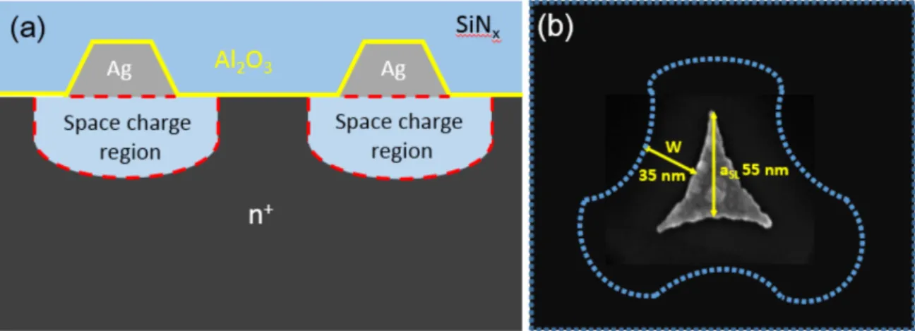
Figure 9(a) illustrates a schematic representation of the
Ag-NPs/Si contact. The depleted zone associated with the contact plays the same role as a depleted region associated with fixed charges. Its extension W is given by [1]:
e e = ( ) w V qN 2 , 3 r b D 0
where εo is the dielectric constant of the vacuum, εr is the
relative dielectric constant of Si, equal to 11.7, q is the electron charge and Vbis the Ag/Si(n) Schottky barrier height
equal to 0.75 eV[1]. Over 500 nm depth, the average value of
NDis 1018cm−3, leading to W equal to 35 nm.
The extension of this depleted layer is illustrated in figure9(b) with over a distance of W. The effective depleted
surface can be associated with a surface based on NPs with an effective size aslincreased by 2 W. The surface S of a NP is
0.04D2 and asl=0.233D [40], giving S=0.736 asl2. The
effective surface Seff of a depleted region associated with a
NP is therefore 0.736 (asl+2 W)2. The gain for the
passi-vated layer, associated with the Ag_NPs space charge region is therefore Seff/S. Starting with a Ag surface coverage r, the
final effective Schottky passivated surface coverage reffis:
=
(
+)
( ) r r 1 W . 4 a eff 2 2 slTaking the experimental surface coverage r of Ag-NPs to 10%., with asl=55 nm for D=230 nm, we calculate reff
equal to 0.53. As the remaining 47% of the surface is also covered by Al2O3, the equivalent depleted depth ZAgNPs
associated with embedded Ag-NPs, calculated all over the surface S, is given by the relation:
* = *( + ) ( )
S ZAgNPs S 0.53 W 0.47ZAl O2 3. 5 This leads to ZAgNPsranging from 20.9 to 23.2 nm, i.e. an
average value of ∼22 nm, which has to be compared with ZAl O2 3 ranging from 5 to 10 nm. As described in the previous
section, the comparison between two passivation processes can be related to the ratio of the depleted regions, equivalent to a ratio of Dit.Thus, the addition of embedded Ag-NPs induces an
equivalent increase of Dit by a typical factor ranging from
22/(5–10), i.e. from 2.2 to 4.4. Finally, the photocurrent I can be now linked to the passivation effect. Indeed, I is inversely proportional to the effective surface recombination velocity Se, while Se varies exponentially with Dit[24].
b
( / ) ( ) ( )
I% 1 Se % exp Dit 6
withβ depending on the sample and on the sign of the fixed charges(the product βDitis positive). It typically ranges from
0.3 to 1 (values deduced by fitting Se versus Dit). Taking for
example β=0.5, we obtain a gain for the photocurrent ran-ging from 3 to 9. The measured gain of 5(figure5) is in that
range, which is thus consistent with the calculated values. As a
Figure 8.TEM image of the Si+Ag-NPs+Al2O3/SiNx:H stacks. In
the inset is shown the interface between Ag-NP and Al2O3/SiNx:H
layers under unfocused approach to separate both layers. The carbon layer on top of the Al2O3/SiNx:H stacks has been added for FIB
result, such analysis allows us to describe, explain and confirm quantitatively the enhancedfield effect passivation induced by the local Schottky Ag-NPs/Si contacts.
4. Conclusion
In conclusion, we have developed a composite structure of ordered Ag-NP arrays embedded in ALD-Al2O3
/PECVD-SiNx:H stacks to improve the absorption and thefield effect
passivation of Si junctions. The density and surface coverage of Ag-NPs were well controlled by using a nanosphere lithography technique to achieve optimal light absorption. Photoconductivity studies of junctions were performed, while the best result was obtained in junctions with Ag-NPs embedded in Al2O3/SiNx:H stacks, giving five times gain
comparing with the only Al2O3/SiNx:H-passivated junction.
Finally, FDTD simulations and semi-quantitative calculations demonstrated that such improvement was mainly due to the enhancedfield effect passivation through the depleted region associated with the Ag-NPs/Si Schottky contacts, in addition to a weak plasmonic effect induced by Ag-NPs. Note that this concept is general and can be extended to other metal. The results achieved here demonstrate that the integration of Ag-NPs in an effective passivation stacks can be easily feasible, and is a really promising approach to increase significantly the efficiency of future solar cells.
Acknowledgments
This work was supported by the‘GENESE’ contract (Ref: 13-BS09-0020-03) from the Agence Nationale de la Recherche, ANR (France) and by the National Natural Scientific Foun-dation of China (61775130). X Portier is grateful to the 〈〈Agence Nationale de la Recherche〉〉 in the framework of the PAI program(ANR-11-EQPX-0020).
ORCID iDs
T Xu https://orcid.org/0000-0003-1410-9261
References
[1] Sze S M 1969 Physics of Semiconductor Devices (New York: Wiley) ch 1
[2] Faltakh H, Bourguiga R, Rabha M B and Bessais B 2014 Simulation and optimization of the performance of multicrystalline silicon solar cell using porous silicon antireflection coating laye Superlattices Microstruct.72 283 [3] Zhou D, Pennec Y, Rouhani B D, Robbe O C, Xu T,
Lambert Y, Deblock Y, Faucher M and Stiévenard D 2014 Optimization of the optical properties of nanostructured silicon surfaces for solar cell applications J. Appl. Phys.115
134304
[4] Salman K A, Omar K and Hassan Z 2012 Effective conversion efficiency enhancement of solar cell using ZnO/PS antireflection coating layers Sol. Energy86 541
[5] Stuart H R and Hall D G 1996 Absorption enhancement in silicon-on-insulator waveguides using metal islandfilms Appl. Phys. Lett.69 2327
[6] Mandal P and Sharma S 2016 Progress in plasmonic solar cell efficiency improvement: a status review Renew. Sustain. Energy Rev.65 537
[7] Atwater H A and Polman A 2010 A single-layer wide-angle negative-index metamaterial at visible frequencies Nat. Mater.9 205
[8] Jang Y H, Jang Y J, Kim S, Quan L N, Chung K and Kim D H 2016 Plasmonic solar cells: from rational design to mechanism overview Chem. Rev.116 14982
[9] Fahr S, Rockstuhl C and Lederer F 2009 Metallic nanoparticles as intermediate reflectors in tandem solar cells Appl. Phys. Lett.95 12105
[10] Rockstuhl C and Fahr Sand Lederer F 2008 Absorption enhancement in solar cells by localized plasmon polaritons J. Appl. Phys.104 123102
[11] Matheu P, Lim S H, Derkacs D, Mcpheeters C and Yu E T 2008 Metal and dielectric nanoparticle scattering for improved optical absorption in photovoltaic devices Appl. Phys. Lett.93 113108
[12] Wang X Y, Wang J L and Wang H 2014 Improvement of the efficiency and power output of solar cells using
nanoparticles and annealing Sol. Energy101 100
[13] Jang Y H, Jang Y J, Kim S, Quan L N, Chung K and Kim D H 2016 Plasmonic solar cells: from rational design to mechanism overview Chem. Rev.116 14982
[14] Liu J, Chen C Y, Yang G S, Chen Y S and Yang C F 2017 Effect of the fabrication parameters of the nanosphere lithography method on the properties of the deposited Au-Ag nanoparticle arrays Materials10 381
[15] Gao P, He J, Zhou S, Yang X, Li S, Sheng J, Wang D, Yu T, Ye J and Cui Y 2015 Large-area nanosphere self-assembly by a micro-propulsive injection method for high throughput periodic surface nanotexturing Nano Lett.15 4591 [16] Aberle A G 2000 Surface passivation of crystalline silicon
solar cells: a review Prog. Photovolt., Res. Appl.8 473 [17] Centeno A, Breeze J, Ahmed B, Reehal H and Alford N 2010
Scattering of light into silicon by spherical and hemispherical silver nanoparticles Opt. Lett.35 76 [18] Jeong S, McGehee M D and Cui Y 2013 All-back-contact
ultra-thin silicon nanocone solar cells with 13.7% power conversion efficiency Nat. Commun.4 2950
[19] Carnel L, Dekkers H F W, Gordon I, Gestel D V,
Nieuwenhuysen K V, Beaucarne G and Poortmans J 2006 Study of the hydrogenation mechanism by rapid thermal anneal of SiN:H in thin-film polycrystalline-silicon solar cells IEEE Electron Device Lett.27 163–5
[20] Otto M, Kroll M, Käsebier T, Lee S M, Putkonen M, Salzer R, Micleaand P T and Wehrspohn R B 2010 Conformal trans-parent conducting oxides on black silicon Adv. Mater.22 5035 [21] Lee H, Tachibana T, Ikeno N, Hashiguchi H, Arafune K,
Yoshida H, Satoh S, Chikyo T and Ogura A 2012 Interface engineering for the passivation of c-Si with O3-based atomic
layer deposited AlOxfor solar cell application Appl. Phys.
Lett.100 143901
[22] Wang W C, Lin C W, Chen H J, Chang C W, Huang J J, Yang M J, Tjahjono B, Huang J, Hsu W C and Chen M J 2013 Surface passivation of efficient nanotextured black silicon solar cells using thermal atomic layer deposition ACS Appl. Mater. Interfaces5 975211
[23] Terlinden N M, Dingemans G, Van de Sanden M C M and Kessels W M M 2010 Role offield-effect on c -Si surface passivation by ultrathin(2–20 nm) atomic layer deposited Al2O3Appl. Phys. Lett.96 112101
[24] Dingemans G and Kessels W M M 2012 Status and prospects of Al2O3-based surface passivation schemes for silicon solar
cells J. Vac. Sci. Technol. A30 040802
[25] Mack S, Wolf A, Brosinsky C, Scmeisser S, Kimmerle A, Cast P S, Hofmann M and Biro D 2011 Silicon surface passivation by thin thermal oxide/PECVD layer stack systems IEEE J. Photovolt.1 135
[26] Schmidt J, Veith B and Brendel R 2009 Effective surface passivation of crystalline silicon using ultrathin Al2O3films
and Al2O3/SiNxstacks Phys. Status Solidi3 287
[27] Veith B, Werner F, Zielke D, Brendel R and Schidt J 2011 Comparison of the thermal stability of single Al2O3layers
and Al2O3/SiNxstacks for the surface passiviation of silicon
Energy Procedia8 307
[28] Dawei W, Rui J, Wuchang D, Chen C, Deqi W, Wei C, Haofeng L, Huihui Y and Xinyu L 2011 Optimization of Al2O3/SiNxstacked antireflection structures for N-type
surface-passivated crystalline silicon solar cells J. Semiconduct.32 094008
[29] Temple L and Bagnall D M 2013 Broadband scattering of the solar spectrum by spherical metal nanoparticles Prog. Photovolt., Res. Appl.21 600
[30] Yang Y, Pillai S, Mehrvarz H, Kampwerth H, Baillie A H and Green M A 2012 Enhanced light trapping for high efficiency crystalline solar cells by the application of rear surface plasmons Sol. Energy Mater. Sol. Cells101 217
[31] Xu T, Tian Z H, Elmi O, Krzeminski C, Robbe O, Lambert Y, Yakeda D, Okada E, Wei B and Stiévenard D 2017 Optical and electrical properties of nanostructured implanted silicon n+-p junction passivated by atomic layer deposited Al2O3
Physica E93 190
[32] Yee K S 1966 IEEE Trans. Antennas Propag.14 302
[33] Zhou D, Xu T, Lambert Y, Robbe O C and Stiévenard D 2015 Enhancement of electrical properties of nanostructured polysilicon layers through hydrogen passivation J. Nanosci. Nanotechnol.15 9772
[34] Lambert Y, Zhou D, Xu T, Cristini O, Deresmes D,
Grandidier B and Stiévenard D 2013 Progressive multi-layer drop-casting of CdSe nanoparticles for photocurrent down shifing monitoring Appl. Phys. Lett.103
051102
[35] Loozen X, Larsen J B, Dross F, Aleman M, Bearda T,
O’Suilvan B J, Gordon I and Poortmans J 2012 Passivation of a metal contact with a tunneling layer Energy Procedia21
75
[36] Ferry V E, Munday J N and Atwater H A 2010 Design considerations for plasmonic photovoltaics Adv. Mater.
22 4794
[37] Stuart H R and Fall D G 1999 Island size effects in nanoparticle-enhanced photodetectors Appl. Phys. Lett.
73 3815
[38] Werner F, Veith B, Zielke D, Kühnemund L, Tegenkamp C, Seibt M, Brendel R and Schmidt J 2011 Electronic and chemical properties of the c-Si/Al2O3interface J. Appl.
Phys.109 113701
[39] Kotipalli R, Delamare R, Poncelet O, Tang X, Francis L A and Flandre D 2013 Passivation effects of atomic-layer-deposited aluminum oxide EPJ Photovolt.4 45107
[40] Hulteen J C and Van Duyne R P 1995 Nanosphere lithography: a materials general fabrication process for periodic particle array surfaces J. Vac. Sci. Technol. A13 1553