HAL Id: hal-01225345
https://hal.archives-ouvertes.fr/hal-01225345
Submitted on 6 Nov 2015
HAL is a multi-disciplinary open access
archive for the deposit and dissemination of
sci-entific research documents, whether they are
pub-lished or not. The documents may come from
teaching and research institutions in France or
abroad, or from public or private research centers.
L’archive ouverte pluridisciplinaire HAL, est
destinée au dépôt et à la diffusion de documents
scientifiques de niveau recherche, publiés ou non,
émanant des établissements d’enseignement et de
recherche français ou étrangers, des laboratoires
publics ou privés.
Coupling study in smart power mixed ICs with a
dedicated on-chip sensor
Marc Veljko Thomas Tomasevic, Alexandre Boyer, Sonia Ben Dhia, Alexander
Steinmar, Weiss B., Ehrenfried Seebacher, Rust P.
To cite this version:
Marc Veljko Thomas Tomasevic, Alexandre Boyer, Sonia Ben Dhia, Alexander Steinmar, Weiss B., et
al.. Coupling study in smart power mixed ICs with a dedicated on-chip sensor. EMC Europe 2015,
Aug 2015, Dresden, Germany. �10.1109/ISEMC.2015.7256236�. �hal-01225345�
Coupling Study in Smart Power Mixed ICs
with a dedicated On-Chip sensor
V.Tomasevic, A. Boyer, S. Bendhia
CNRS, LAAS, 7 avenue du colonel Roche, F-31400
Toulouse, France
Univ. de Toulouse, INSA, LAAS, F-31400 Toulouse,
France
Contact: [email protected]
A. Steinmair, B. Weiss, E. Seebacher, P. Rust
ams AG,
Tobelbaderstrasse 30, 8141 Unterpremstätten,
Austria
Abstract— In order to merge low power and high voltage devices
on the same chip at competitive cost, Smart Power integrated circuits (ICs) are extensively used. Electrical noise induced by power stage switching or external disturbances generates parasitic substrate currents, leading to a local shift of the substrate potential which can severely disturb low voltage circuits. Nowadays this is the major cause of failure of Smart Power ICs, inducing costly circuit redesign. Modern CAD tools cannot accurately simulate this injection of minority carriers in the substrate and their propagation in the substrate. In order to create a link between circuit design, modelling and implementation in innovative CAD tools there is a need to validate these models by measuring the high voltage perturbations that activate parasitic structures in the substrate directly on the chip. This paper presents an on-chip noise sensor dedicated to measurements of transient voltage fluctuations induced by high voltage activity and coupled by the substrate.
Keywords — on-chip sensor; Smart Power IC; substrate noise coupling; electromagnetic compatibility; substrate parasitic bipolar structures;
I. INTRODUCTION
Nowadays, many segments of microelectronics move towards monolithic system integration merging on the same IC (Smart power ICs) low voltage analog and/or digital parts with high voltage parts using power transistors.
Substrate coupling in Smart power ICs occurs when parasitic bipolar structures (with unpredictable size and location) are activated after an injection of current into the substrate due to internal switching activity or external noise coupling. When low power analog and digital applications are integrated with high voltage (HV) devices on the same IC, these side effects become very important and hurtful to the circuit operation. In turn, designers have to rely on empirical basis for the design strategy, which is expensive and time consuming. Today, when simulating circuits with HV-MOSFETS devices, their specific SPICE models are used in every CAD tool but these models do not address generation of these parasitic substrate currents of minority and majority carriers.
AUTOMICS project [1] aims at providing SPICE models, once implemented in CAD tools, will allow optimizing high voltage and high current capability, EMI-EMC performance
with respect to substrate parasitic robustness. Moreover, AUTOMICS should considerably improve the design methodology by developing efficient CAD models of parasitic structures activated by HV functions integrated in automotive Smart Power ICs [1]. In order to detect parasitic bipolar structures activation and the induced substrate coupling effect, some measurements have to be done directly on internal sensitive nodes using an on-chip sensor and thereby validate the proposed Spice models of the parasitic bipolar junction. These measurements will be performed with a dedicated on-chip sensor, specially designed for the AMS H35, High Power 0.35µm technological process. Other versions of the sensor were realized in order to characterize the integrity of the high speed signals (parasitic coupling issues between high speed lines, the delay induced by parasitic coupling) adapted for the 0.25µm Smartmos 8 technology [4], [5]. The architecture and sampling method between different versions of the sensor stays the same but in order to have similar performances on different technological processes some adjustments were done.
This paper aims at presenting an on-chip sensor dedicated to the characterization of transient voltage fluctuations due to parasitic structures activation in real application conditions. Section II briefly presents substrate-coupling issues in Smart Power ICs. Section III introduces the principles and structure of the proposed on-chip sensor. Section IV presents experimental measurements of substrate coupling effects on sensitive nodes in a Smart Power IC.
II. SUBSTRATE COUPLING ISSUES IN SMART POWER ICS
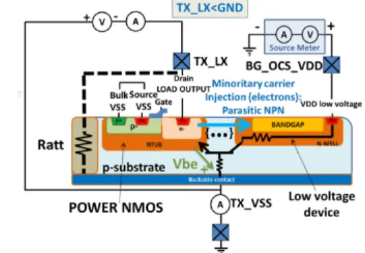
In Smart Power ICs, sources of substrate coupling are parasitic NPN and PNP bipolar transistors (Fig. 1) activated by ‘below-ground’ or ‘above-supply’ working conditions of High Voltage-MOSFETS at the circuit output [2], [3]. These parasitic bipolar transistors can be activated during normal circuit operation by the switching on/off of inductive loads. They can be also activated during usual automotive chip testing (EMI-EMC tests), by external electromagnetic perturbations or electrostatic discharges.
Two physical mechanisms are behind this type of coupling as seen in Fig.1. The first one is the injection of holes (majority carriers) into the p substrate (Fig. 1a). This happens when the drain of the power PMOS (i.e. the power output of the circuit), exceeds the power supply voltage VDD,
activating a parasitic PNP transistor. This in turn leads to a local voltage shift of the substrate potential in the neighbor sensitive electronic blocks. The second physical mechanism is the injection of electrons (minority carriers) into the p substrate when the drain of the power NMOS, at the power output of the circuit, is below the ground potential and thus activates a parasitic NPN transistor (Fig. 1.b).
These minority carriers injected into the substrate can be collected by every surrounding NTUB and causing a voltage fluctuation of the N-WELL of a surrounding sensitive blocks and cause its dysfunction.
a.)
b.)
Fig. 1 Wafer cross section of power a.)PMOS b.)NMOS
III. ON-CHIP SENSOR :PRINCIPLE &STRUCTURE
A. A general description
The on-chip sensor was developed to address signal and power integrity issues at circuit level, like an on-chip oscilloscope. Based on a sequential equivalent-time sampling method, the sensor exploits the benefits of subsampling techniques, which ensure a very high virtual sample rate without severe constraints on hardware bandwidth like in high speed sampling circuits. The signal to measure has to be repeatable and synchronized with the sampling command of the sensor [4], [5]. The on-chip sensor has its dedicated 5V power supply as a critical and crucial requirement to avoid any external disturbances and noise produced of other blocks of the circuit architecture description.
External disturbances and noise produced of other blocks of the circuit can induce voltage fluctuations coupled on sensor-on chip power supply and its substrate reference. This in turn can alter measurements and thus isolating the sensor of other circuit blocks is a critical and crucial requirement. With the present on-chip sensor, due to its internal architecture, the measurements can be done with minimal alteration of the circuit operation i.e. by adding high parasitic capacitance and/or small resistance on sensitive nodes.
B. Architecture description
The on-chip sensor architecture, presented on Fig. 2., is composed of an analog/digital core cell used to control 8 sensor probes placed close to nodes monitored during the test [4], [5]. Each probe is composed of one Sample&Hold (S&H)
cell, followed by a folded cascode operational amplifier in buffer configuration.
Fig. 2 Sensor-on chip architecture
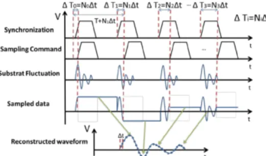
The sensor core integrates an 8x1 analog multiplexer (to externally select one of the 8 probes), a folded cascode operational amplifier in the buffer configuration and a delay cell used to control the acquisition time. The delay cell, used for subsampling method, provides a programmable sampling command with a variable delay added to the falling edge of the synchronization signal by a delay ∆Ti [4], [5]. The principle of subsampling method and the signal reconstruction are described in Fig. 3. The control of the delay is done by two external analog signals: the Vrange signal shapes the time range
for the delay, while the Vanalog signal ensures the delay fine
control. The delay law varies between 50ns and 1200ns. Delay cell characteristic after a calibration is shown on Fig. 4.
Fig. 3 The subsampling principle and the reconstruction of the temporal
Fig. 4 Delay cell characteristics (measurements)
The input voltage range of a nominal (without attenuator) is between 0.3 V and 4 V. For high voltage measurements an attenuator is placed at the input of the probe. To ensure low intrusion during voltage measurements the S&H cell (with the optional attenuator) form a high impedance probe with input capacitance of 25fF and a bandwidth of 1.7GHz.
Due to imperfections and mismatch in the implementation of the on-chip sensor, calibration procedures have to be performed. The sensor imperfections can be easily compensated by post-processing from the transfer function characterization.
IV. STUDY OF SUBSTRATE COUPLING ISSUES IN SMART POWER
CIRCUITS
The on-chip sensor is now used to study substrate coupling effect in Smart Power IC. The proposed study focuses on typical sensible devices and structures used in 0.35µm ams High Voltage CMOS technology using an 20V mixed signal process with 3 metal layers. This technology permits to isolate low voltage transistors, with a buried N-WELL, from high voltage part of the circuit. As already mentioned the sensor had to be entirely designed with 5V isolated MOS transistors. The entire test circuit is on the same die : the on chip sensor, one DC-DC converter and two bandgaps. One bandgap is provided with the sensor probes on its sensitive nodes and another bandgap without sensor probes which is used to verify if the sensor affects the bandgap operation (bandgap output voltage, power consumption). No major differences are observed between both bandgap. The circuit is mounted in a 32 QFN package, and soldered on a four-layer EMC test board with all surrounding electronics and I/O connections.
Sensor measurements aim at determining the amount of coupling between a power part (the output stage of a DC-DC converter) and a low voltage analog part (bandgap reference voltage). Two sensor probes (S4 & S5), have been placed on the DC-DC converter output in order to measure its transient voltage profile, and if needed transient current profile (not used here, only measurements with probe S4 will be considered). Three other sensor probes are placed on the bandgap sensitive nodes (the probe S6 on bandgap guard ring BG_DNPS, the probe S7 on bandgap output, and the probe S8 on bandgap power supply), in order to measure the impact of substrate coupling on this structure. TABLE I. gives the characteristics of these sensors.
Table I
PROBES S4,S5,S6,S7AND S8CHARACTERISTICS
Probe No. Probe Location Input signal range Attenuation ratio
Probe S4 DC-DC output 2V to 28V 1/7 Probe S5 DC-DC output 2V to 28V 1/7 Probe S6 Bandgap N-WELL (guard ring) 0.3V to 4V 1/1 Probe S7 Bandgap output 0.3V to 4V 1/1 Probe S8 Bandgap VDD 0.3V to 4V 1/1
Three case studies are intended in this work. The first one is done during nominal circuit operation and consists in observing the coupling between a power device (DC-DC converter) and a low voltage analog block (1.23V bandgap reference voltage circuit, later bandgap). The second experiment, done by inducing an external electromagnetic perturbation, has the purpose to measure the coupling and the impact of the current injection on the output of the power device (DC-DC converter) to the low voltage block (bandgap).
A. Coupling between power and low voltage analog block
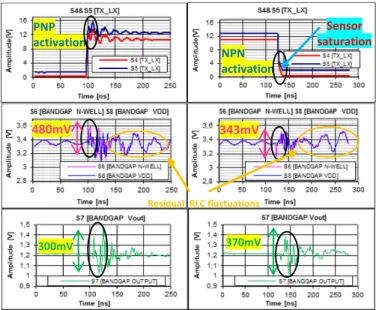
The objective of the experiment presented on Fig. 5 is to observe disturbances induced by the switching of one DC-DC converter on a bandgap circuit. Measurements are done directly on the DC-DC converter outputs (sensor probes S4
and S5) and also directly on the bandgap circuit sensitive nodes as its N-WELL, its output, and on its low voltage power supply (sensor probes S6, S7 and S8 respectively).
Fig. 5 Coupling between power and low voltage analog blocks
During switching operation of the DC-DC converter, on-chip sensor measurements, presented on Fig. 5, show that some noise appears on the bandgap sensitive nodes. The noise amplitude is linked to the DC-DC converter power supply voltage (TX_VDD20) and the switching current (related to the load resistance and inductance). Due to the high temporal resolution of the on-chip sensor measurements (in comparison to oscilloscope measurements), the observed voltage fluctuations on the bandgap sensitive nodes leads us to a better understanding of the coupling mechanism present in Smart Power ICs.
Fig. 6 DC-DC output effects on Bandgap power supply and output (left colon: rising edge; right colon: falling edge)
The voltage overshoot above the high voltage power supply is observed on the rising edge of the DC-DC converter output signal; more precisely on the drain of the conducting output power PMOS. This effect is the source of the activation of the parasitic PNP transistor leading to a local positive voltage shift of the substrate. Thus surrounding bandgap N-WELL has also a positive voltage shift relative to this voltage shift. As a consequence, bandgap power supply and its output have the same initial signal shape of this perturbation. The residual following fluctuations are caused by the resonance of the power supply RLC network. The bandgap output signal is also disturbed by these residual fluctuations of its power supply voltage, but in much less amount as expected due to his high power supply rejection ratio.
300mV 370mV 480mV 343mV PNP activation NPN activation Sensor saturation Residual RLC fluctuations
On the other side, when a falling edge occurs at the DC-DC converter output (probes S4 & S5 saturates below 0,4V), the drain of the conducting output power NMOS have a similar below ground voltage overshoot. This effect leads to the activation of the parasitic NPN transistor and is the source of a local negative voltage shift of the substrate potential. Surrounding bandgap N-WELL collects the substrate current and has also a negative voltage shift. Thus, bandgap power supply and its output have the same initial signal shape of this perturbation and the residual following fluctuations are also caused by the resonance of the substrate RLC network. Again, the bandgap output signal is also disturbed by these residual fluctuations of its power supply voltage, but in much less amount as expected due to his high power supply rejection ratio.
B. Influence of an EMI injected on DC-DC output stage on bandgap
In the experience presented on Fig. 7, the output of the DC-DC converter (TX_LX pin) harmonic disturbances are coupled in order to simulate the coupling of an electromagnetic interference test (EMI injection test). In real conditions the potentially mechanical large load or long cables connected to the output of the DC-DC converter may couple a significant amount of electromagnetic disturbance.
Fig. 7 Description of the conducted EMI test
Two sets of EMI injection tests were performed. Firstly the DC-DC converter power supply voltage (TX_VDD20) is set to 12 V without any resistive load on its output and the output PMOS was activated. The aim of this setup is to observe the activation of the parasitic PNP bipolar transistor. Afterwards the DC-DC converter was disabled and the tests were performed around the ground voltage in order to observe the activation of the parasitic NPN transistor. For both sets of tests, the on-chip measurements are performed will be done directly on the DC-DC converter outputs (sensor probe S4) and also directly on the bandgap circuit sensitive nodes as its N-WELL, its output, and on its low voltage power supply (sensor probes S6, S7 and S8 respectively).
1) Activation of the parasitic PNP bipolar transistor
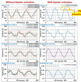
The first set of tests has been performed with various disturbance amplitudes and with power supply voltage set to 12 V. The measurements show very well the nature of the coupling between the DC-DC converter output and the bandgap sensitive node and they highlights the role of the substrate coupling mechanism and especially the role of the PN junction between the drain of the PMOS device of the DC-DC converter output and the surrounding N-WELL. Depending on the amplitude of the disturbance, the nature of the coupling may change as we can see on Fig. 8.
Fig. 8 PNP activation by EMI test on chip measurements of in presence of a 10 MHz disturbance with different Power Forward values
(PFOR=25.88dBm; 27,88dBm; 30.99dBm; 32.41dBm)
2) Activation of the parasitic NPN bipolar transistor
The second set of tests, shown in Fig. 8, has been also performed with various disturbance amplitudes and with the DC-DC converter disabled and thus having the power PMOS and NMOS in tristate mode. The measurements show very well the nature of the coupling between the DC-DC converter output and the bandgap output node, as a very sensitive node. This test highlights the role of the substrate coupling mechanism and especially the role of the PN junction between the drain of the NMOS device of the DC-DC converter output and the surrounding N-WELL of low power devices, like a bandgap present in our test chip. Here, in order to have a better coupling mechanism, the N-WELL guard ring of the bandgap was not polarized to minimizing the amount of electrons collected on it. This shows more accurately the coupling mechanism of the substrate coupling, when electrons injected into the substrate produces a voltage shift of internal bandgap sensitive nodes which in turn leads to an offset to its output and even more, when higher input injection power occurred, a deformed signal at the output of the bandgap can be observed.
Fig. 9 NPN activation by EMI test on chip measurements of in presence of a 10 MHz disturbance with different Power Forward values
(PFOR=25.88dBm; 30dBm; 33dBm; 35dBm; 37.77dBm)
PNP activation
Without bipolar activation With bipolar activation
With bipolar activation Without bipolar activation
We can observe from last figure Fig. 9 that depending on the amplitude of the disturbance, the nature of the coupling may change. Also a small, but not negligible, offset on the bandgap output can be observed depending on the amplitude of the disturbance. Note that due to the sensor limitations we cannot observe signals under 2V with probes S4 and S5, because they have a 1/7 attenuator on their inputs (see Table I) so here they are not provided. Because the bandgap N-WELL wasn’t polarized, measurements with probe S6 were also not provided here.
3) General observations for EMI test on chip measurements
From the previous measurement results the effects on the signals on the DC-DC converter output (TX_LX) and on bandgap internal signals are quite complicated to be fully described as they are dependent on the EMI amplitude and frequency. Nevertheless some interesting general conclusions can be drawn and two issues can be determined.
For both sets of tests, small voltage fluctuations amplitude coupled on TX_LX node, below a threshold voltage Vthreshold
above the power supply voltage TX_VDD20 or under the ground, the measured signals are not distorted. It can be noticed that a part of this disturbance is coupled on the internal signals of the bandgap and has the same shape as the input disturbance and the amplitude and phase of these internal bandgap signals are related to the input frequency. By doubling the disturbance amplitude the induced voltage amplitude, induced within the bandgap is also doubled, showing the linearity of the coupling effects. These effects can be associated to parasitic RLC network of the substrate and/or a coupling by the power distribution network and can’t be caused by a substrate coupling mechanism with parasitic bipolar transistor activation as described before. Nevertheless, the impact on the integrity of the output voltage of the bandgap remains weak or moderate.
On the other side, for the first set of tests, when voltage fluctuations amplitude coupled on TX_LX node are “large enough” and exceeds a threshold voltage Vthreshold above the
power supply voltage TX_VDD20 (nearly equal to the threshold voltage of a PN junction) the measured signals are distorted. Also, for the second set of tests when voltage fluctuations amplitude coupled on TX_LX node are “large enough” and exceeds a threshold voltage Vthreshold under the
ground voltage (nearly equal to the threshold voltage of a PN junction) the measured signals are distorted. This distortion of coupled signals on the bandgap sensitive nodes is due: -for the first set of tests, to the activation of the parasitic PNP transistor caused by an above power supply condition on the drain of the PMOS transistor of the DC-DC converterpower output;
-for the second set of tests, the activation of the parasitic NPN transistor caused by an under power supply condition on the drain of the NMOS transistor of the DC-DC converterpower output;
The surrounding N-WELL of the bandgap device fluctuates too, but the shape of the signal is distorted clearly showing that the current within the substrate triggers the activation of the parasitic PN junctions. The bandgap power supply and its
output fluctuates too and their signal shape showing a non-linear regime of this type of coupling. As a result, the integrity of the output voltage of the bandgap gives voltage fluctuations of several tens up to hundreds of millivolts and generation of voltage offsets.
C. I(V) characterisation of the parasitic bipolar structures
In this experiment the aim is to activate the parasitic bipolar structures and characterize them using a four quadrants source meter. In order to obtain characteristic I(V) curves of these parasitic bipolar transistors, the source meter is used to inject the current into the substrate of the test circuit: by controlling both current and voltage at the output and power supply pins of the test circuit the effects of an inductive charge can be simulated for instance. Two cases studies are analysed: one intended to activate the parasitic PNP transistor, see Fig. 10, and another to activate the parasitic NPN, see Fig. 11.
In this experience the DC-DC converter was disabled in order to have both PMOS and NMOS output transistors in tristate mode and avoid their damaging, even their destruction. Here, the Ratt resistance stands for the equivalent resistance of
the input attenuators of the On-Chip Sensor probes S4 and S5 and was experimentally measured.
Fig. 10 I(V) characterisation of parasitic bipolar a.)PNP b.)NPN transistor
Fig. 11 I(V) characterisation of parasitic bipolar NPN transistor
As seen before, in order to activate the parasitic PNP transistor, the power PMOS drain (the TX_LX output pin) needs to be at least above the power supply (TX_VDD20 pin) plus a threshold voltage Vthreshold. The threshold voltage
corresponds to the voltage of a forward biased diode formed by the p well of the NMOS drain and the n well of the NTUB.
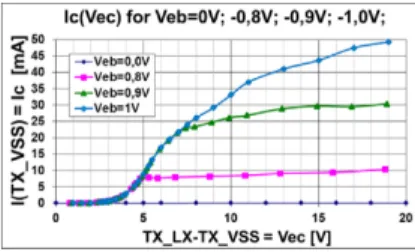
In the figure below, Fig. 11, we can observe a characteristic transfer curve Ic(Vec) of a PNP transistor for 3 different
voltage values of Veb=V(TX_VDD20)-V(TX_LX). Obviously, the transfer curve corresponds to the parasitic PNP transistor considered in our work. As expected, the current Ic increase with higher Veb values.
Fig. 12 Parasitic PNP characteristic transfer curve Ic(Vec) for different values of Veb
Next step is to analyze the activation of the parasitic NPN transistor by biasing the drain (TX_LX output pin) of the power NMOS transistor below the ground voltage. The threshold voltage of a forward biased diode formed by the n well of the PMOS drain and the p well of the p-substrate is measured at Vbe= -0.4 V. The effects of these working conditions are observed on the bandgap output in the figure below, Fig. 12.
Fig. 13 Parasitic NPN characteristic transfer curves Ie(Vbe) and Ic(Vce)
Fig. 14 Influence on bandgap output of the Vbe=V(TX_LX) voltage of the parasitic NPN transistor
On the previous figure, on the right on the Fig. 13, the Ic(Vce) transfer curve clearly demonstrate the supposition of the activation of the parasitic NPN transistor. This activation is due to the minority carrier injection into the p type substrate when the drain (TX_LX pin) of the output NMOS goes below ground voltage. This in turn induces the current to flowing outside of the chip, as seen on Ie(Vbe) transfer curve, the left part of the Fig. 13.
The main consequence of the activation of the parasitic bipolar NPN transistor, the bandgap output increases from nominal 1.2V to about its supply voltage of 3.3V progressively, leading to its dysfunction. This is essentially due to the increasing of the current inside the current mirrors present in the bandgap circuit architecture, which in turn is
transferred to its output due to the false biasing of its transistors used as reference voltage source.
V. CONCLUSIONS
This paper presents an on-chip sensor dedicated to the analysis of substrate coupling issues in Smart Power ICs. On-chip sensor offers a more accurate evaluation of these substrate coupling issues than a simple oscilloscope measurements without the possibility to scan IC internal nodes. This on-chip sensor has the advantage to perform low intrusion voltage measurements with high temporal resolution, have a large bandwidth obtained by subsampling technique and due to its separated power supply and its closeness to the measured point any additional noise coupling from other circuit blocks is avoided.
The first experiment clearly shows the effect of substrate coupling mechanism in Smart Power Ics when the DC-DC converter output is switching causing a coupling on bandgap critical nodes. Both coupling mechanism are observed and the activation of the parasitic PNP and NPN transistor are demonstrated. The amount of substrate coupling is linked to the DC-DC converter power supply voltage and its switching current. With the second experiment, the EMI injection tests on the output of the DC-DC converter, the analysis of the results confirms the major importance of the parasitic PN junction activation in the coupling between the DC-DC converter output and a neighbour bandgap reference voltage. With the last experiment a deeper analysis was performed in order to characterise these parasitic PNP and NPN transistors and the obtained I(V) transfer curves clearly show their presence and activation. Their activation consequence to the low voltage bandgap structure confirms again that the coupling via the substrate current has a major importance of the parasitic PN junction activation.
Acknowledgment
This study has been done with the financial support of FP7 Programme, a funding programme created by European Union (project AUTOMICS with grant agreement no. 314135).
References
[1] (2014) The AUTOMICS web site [Online]. Available: https://www.automics.eu/
[2] F. Lo Conte, J.-M. Sallese, M. Pastre, F. Krummenacher and M. Kayal. “A circuit-level substrate current model for smart-power ICs, IEEE Transactions on Power Electronics”, vol. 25, num. 9, p.2433-2439, 2010.
[3] M. Schenkel, “Substrate Curent Effects in Smart Power ICs”, Ph.D thesis, 2003, Technische Wissenschaften ETH Zürich, Nr. 14925, Available from: e-collection.library.ethz.ch, pp 1-24.
[4] S. Ben Dhia, “Une nouvelle methodologie de caracterisation de l’integrite du signal en cmos submicronique profond.” Ph.D thesis, 2003, Institut national des sciences appliquées de Toulouse.
[5] S. Ben Dhia, A; Boyer, “On-Chip Noise Sensor for Integrated Circuit Susceptibility Investigations” IEEE transactions on instrumentation and measurement, vol. 61, no. 3, march 2012