HAL Id: cea-01757656
https://hal-cea.archives-ouvertes.fr/cea-01757656
Submitted on 3 Apr 2018
HAL is a multi-disciplinary open access
archive for the deposit and dissemination of
sci-entific research documents, whether they are
pub-lished or not. The documents may come from
teaching and research institutions in France or
abroad, or from public or private research centers.
L’archive ouverte pluridisciplinaire HAL, est
destinée au dépôt et à la diffusion de documents
scientifiques de niveau recherche, publiés ou non,
émanant des établissements d’enseignement et de
recherche français ou étrangers, des laboratoires
publics ou privés.
Smart Instruction Codes for In-Memory Computing
Architectures Compatible with Standard SRAM
Interfaces
Maha Kooli, Henri-Pierre Charles, Clément Touzet, Bastien Giraud,
Jean-Philippe Noel
To cite this version:
Maha Kooli, Henri-Pierre Charles, Clément Touzet, Bastien Giraud, Jean-Philippe Noel. Smart
In-struction Codes for In-Memory Computing Architectures Compatible with Standard SRAM Interfaces.
Design, Automation and Test in Europe, Mar 2018, Dresde, Germany. �cea-01757656�
Smart Instruction Codes for In-Memory Computing
Architectures Compatible with Standard SRAM
Interfaces
Maha Kooli
1, Henri-Pierre Charles
2, Clement Touzet
1, Bastien Giraud
1, Jean-Philippe Noel
1 1Univ. Grenoble Alpes, CEA, LETI, F-38000 Grenoble
2
Univ. Grenoble Alpes, CEA, LIST, F-38000 Grenoble
[email protected]
Abstract—This paper presents the computing model for In-Memory Computing architecture based on SRAM memory that embeds computing abilities. This memory concept offers significant performance gains in terms of energy consumption and execution time. To handle the interaction between the memory and the CPU, new memory instruction codes were designed. These instructions are communicated by the CPU to the memory, using standard SRAM buses. This implementation allows (1) to embed In-Memory Computing capabilities on a system without Instruction Set Architecture (ISA) modification, and (2) to finely interlace CPU instructions and in-memory computing instructions.
I. INTRODUCTION
In-Memory Computing (IMC) represents a new concept of data computation that has been introduced to overcome the von Neumann bottleneck in terms of data transfer rate. This concept aimes to reduce the traffic of the data between the memory and the processor. Thus, it offers significant reduction of energy consumption and execution time compared to the conventional computer system where the computation units (ALU) and the storing elements are separated. Hardware security improvements can also be expected thanks to this system architecture (e.g., side channel attacks, etc).
The IMC concept has just started to be the focus of recent research works. The objective of our research works is to focus on different technological layers of an IMC system: silicon design, system architecture, compilation and programming flow. This enables to build a complete IMC system that can be then industrialized. In previous publications, we introduced our novel In-Memory Power Aware CompuTing (IMPACT) system. In [1], we presented the IMPACT concept based on a SRAM architecture and the possible in-memory arithmetic and logic operations. In [2], we proposed a dedicated software emulation platform to evaluate the IMPACT system perfor-mance. The results achieved in these papers show a significant performance improvement of the IMPACT system compared to conventional systems. In the present research work, we focus on a new important step of the design of a complete IMPACT system, in particular the communication protocol between the memory and the Computation Processor Unit (CPU).
Fig. 1 presents a comparison of the communication protocol for a conventional system, for a GPU system and for our
CPU Memory IMPACT Memory CPU GPU Memory GPU
…
Sequential computation• Multiple instruction fetch • Multiple data transfer
…
Parallel computation
Parallel computation • Single instruction fetch
• Multiple data transfer
• Single instruction transfer • No data transfer ALU Con ve ntional System GPUs IM PACT 32-bits 32-bits 512-bits Instruction fetch Data transfer Instruction fetch (a) (b) (c) Instruction fetch Data transfer
…
Instruction fetch Data transfer Data transferFig. 1. Comparison between the Communication Protocols of (a) Conven-tional System (von Neumann), (b) System with Accelerators GPUs (von Neumann with Single Instruction Multiple Data (SIMD)) and (c) IMPACT Systems (non von Neumann).
IMPACT system. In a conventional system based on von Neumann architecture, the traffic between the memory and the CPU is very crowded. Several instruction fetches and data transfers occupy the system buses during the computation (Fig. 1.a). In systems that are integrating accelerators (e.g., GPUs), the computation is performed in parallel, whereas only a single instruction fetch is needed. However, data transfers are still required over the data bus (Fig. 1.b). The traffic of our IMPACT system is completely different from the previous systems. No data transfer over the system buses is required since the computation is performed inside the memory. In addition, only one instruction transfer towards the memory
is required (Fig. 1.c). Indeed, the IMPACT system presents a new concept that completely changes the memory features by integrating computation abilities inside the memory boundary. Therefore, the usual communication protocol between the memory and CPU is not fully compatible with the specific IMPACT system architecture. Thus, it has to be redefined to manage the new process of instruction executions.
In this paper, we push one step further our research works on IMPACT system by:
• Introducing a novel communication protocol between the CPU and the memory that is able to manage the transfer of the IMPACT instructions to the memory.
• Defining the ISA that corresponds to this protocol. The reminder of this paper is organized as follows. Sec-tion II provides a summary of the architecture and the com-munication protocol used in conventional system. Section III discusses related works. Section IV introduces the IMPACT instruction codes and the communication protocol. In sec-tion V, we provide a possible solusec-tion to integrate the proposed IMPACT instructions inside an existing processor ISA. Finally, section VI concludes the paper.
II. BACKGROUND
In most traditional computer architecture, the memory and the CPU are tightly connected. Conventionally, a micropro-cessor presents a number of electrical connections on its pins dedicated to select an address from the main memory, and another set of pins to read/write the data stored from/or into that location. The buses which connect the CPU and the mem-ory are one of the defining characteristics of a system. These buses need to handle the communication protocol between the memory and the CPU. The buses transfer different types of data between components. In particular, we distinguish, as shown in Fig. 2, three types:
• Data bus: It has a bidirectional functionality. It enables the transfer of data that is stored in the memory towards the CPU, or vice versa.
• Address bus: It is an unidirectional bus that enables the transfer of addresses from CPU to the memory. When the CPU needs a data, it sends its corresponding memory location via the address bus, the memory then sends back the data via the data bus. When the processor wants to store a data in the memory, it sends the memory location where it will be stored via the address bus, and the data via the data bus.
• Control bus: It is a set of additional signals defining the operating mode, read/write, etc.
Address Bus Central Memory CPU ALU Decoder Reg PC Control Bus Data Bus
Fig. 2. Conventional Computing System Architectures.
When the program is executed, for each instruction the processor proceeds by the following steps:
1) Fetch the instruction from memory: The CPU transmits the instruction address via the address bus, the memory forwards then the instruction stored in that location via the data bus.
2) Decode the instruction using the decoder: The decoding process allows the CPU to determine which instruction will be performed. It consists in fetching the input operands and the opcode, and moving them to the appropriate registers in the register file of the processor. 3) Access memory (in case of read/write instructions): For ’read’instruction, this step consists in sending a memory address on the address bus and receiving the value on the data bus; The ’write’ instruction consists in sending a data with the data bus. Then, this data is copied into a memory address, sent by the address bus. The control bus is used activate the write or read mode.
4) Execute the instruction.
5) Write-back (in case of arithmetic/logic instructions): the ALU performs the computation and write back the result in the corresponding register.
III. RELATEDWORKS A. In-Memory Computing
Processing in-Memory (PiM), Logic in-Memory (LiM) and IMC architectures have been widely investigated in the context of integrating processor and memory as close as possible, in order to reduce memory latency and increase the data transfer bandwidth. All these architectures attempt to reduce the physical distance between the processor and the memory. In Fig. 3, we represent the main differences between PiM, LiM and IMC architectures. PiM [3] [4] [5] consists in putting the computation unit next to the memory while keeping the two dissociated. It is generally implemented in stand alone memories fabricated with a DRAM process. LiM and IMC architectures are based on embedded memories fabricated with a CMOS process. LiM [6] enables distributing non-volatile memory elements over a logic-circuit plane. IMC consists in integrating computation units inside the memory boundary, and represents a different concept that completely changes the memory behavior by integrating some in-situ computation functions located either before or after sens amplifiers circuits. As a result, the communication protocol between the memory and the processor has to be redefined. Compared to LiM, IMC enables non-destructive computing in the memory, i.e., the operand data are not lost after computation. Some recent research works start to explore and evaluate the performance of this concept. It has been applied both on volatile memories [7] [8] [9] and non volatile memories [10] [11].
Most of the existing IMC studies focus on the IMC hard-ware design. The system buses have never been presented, nor interactions between the CPU and the memory. Moreover, no ISA to implement the IMC system architecture has already been defined. All these points clearly limit the conception of a complete IMC system.
CPU SRAM bus Additional Logic On-chip Memory CPU Additional Logic Off-chip Memory Logic in Memory Embedded Memories (CMOS Process)
Stand-alone Memories (DRAM Process)
- Planar/3D process - Non-destructive computing M ulti -r ow Selector - Non-Volatile Memories (ReRAM, …) - Destructive computing - Non Volatile and Volatile Memories - Non-destructive computing n On-chip Memory SRAM SRAM bus n SRAM In-Memory Computing Processing in Memory CPU DRAM bus DRAM
Fig. 3. Comparison between IMC, LiM and PiM Architectures.
In this paper, we focus on the communication protocol between the memory and the CPU for the IMPACT system and we define the ISA. This study is a basic step in the devel-opment of a complete IMC system on different technological layers from the hardware to the software. In addition, the IM-PACT system is able to support operations with multi-operand selection. Thus, the classic format of instruction (opcode + two source operand addresses + a destination address) cannot be used due to limitations in the bus size.
B. Communication Protocols in Computing Systems
The communication protocol between the memory and CPU has been widely presented and discussed in different works [12] [13] [14]. This protocol is implemented and managed using buses. Existing system buses (data bus, address bus, control bus) are generally used to transfer the data or the addresses, but not the instructions. For the IMPACT system, the CPU should communicate the instruction to the memory so that the memory executes/computes this instruction. In the existing computer architecture, the buses are designed to enable only read and write operations, but not arithmetic and logic operations. This paper introduces a new communication protocol that is able to efficiently manage the interaction between the CPU and the IMPACT memory with a full compatibility with the existing buses.
IV. IMPACT MEMORYINSTRUCTIONCODES In this Section, we define the different IMPACT memory instruction codes that will be transmitted by the processor to the memory via the system buses. The challenge is to make
the IMPACT system architecture as close as possible to a conventional system architecture, i.e., we aim to bring the less possible changes to the conventional system implementation in order to facilitate the integration of the IMPACT system to existing system architectures. In addition, it allows to propose a system that is able to interweave the execution of conventional CPU instructions and IMPACT instructions. A. IMPACT Specific Operations
IMPACT system is based on the SRAM architecture to perform operations inside the memory macro thanks to an array composed of bitcells with dedicated read ports. The IMPACT system circuitry enables the same logic and arith-metic operations as a basic ALU. It also presents new specific features that are:
• Multi-Operand Operations: The IMPACT system cir-cuitry is able to perform logic and memory operations not only on two operands as for conventional systems, but on multiple operands. In fact, this feature is achieved thanks to the multi-row selector, which enables to generate a defined selection pattern (e.g., one line out of four, half-top of the rows, etc).
• Long-Word Operations: The IMPACT system circuitry is able to perform arithmetic/logic/memory operations on words whose size can be up to the physical row size of the memory. The operand size is no longer limited by the register size (that is much more smaller that the maximum memory row size).
B. IMPACT Instruction Formats
Regarding these specific features of the IMPACT operations, we propose two new formats that enable to build the IMPACT memory instruction codes.
(a) Multi-Operand Instruction Format: (b) Two-Operand Instruction Format:
Opcode Address Mask SP Output SI Opcode Address 1 Address 2 SP Output SI Fig. 4. Description of IMPACT Instruction Formats.
1) Multi-Operand Instruction Format: The multi-operand format enables to define the structure of the instruction that performs a multi-operand operation. In fact, in conventional system architecture, the instruction size is usually of 32 bits [15]. Thus, they do not enable to encode all the addresses of the multiple operands. Therefore, we propose to define a pattern that enables to select the lines that store the operand data of the given operation. This pattern is built thanks to a pattern code (defined by both an address and a mask) driving a specific row-selector.
To implement this instruction, we propose a multi-operand format, as shown in Fig. 4.a, that encodes:
- The opcode of the operation. In Fig. 6, we provide the list of the logic multi-operand operations that the IMPACT system is able to execute.
- The row selector address. - The row selector mask.
- The output address, where the computation result is stored.
- A Smart Instruction (SI) bit to inform the memory about the instruction type: an IMPACT or a conventional instruction.
- A Select Pattern (SP) bit to enable/disable the pattern construction using the row-selector.
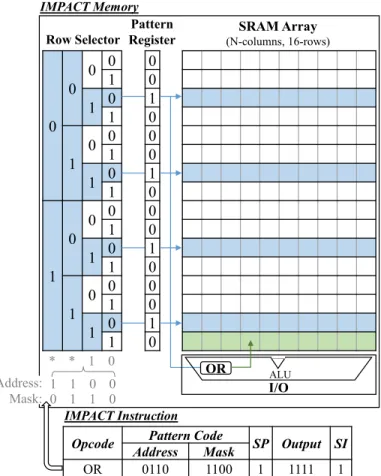
In Fig. 5, we provide an example of the operating mode of the IMPACT system when it is executing a logic ’OR’ operation with multi-operand. As input, the system take the instruction composants (opcode, pattern code, etc). Based on the bits of the pattern code address and mask, the specific row selector of the IMPACT memory builds a regular pattern to select the multiple memory lines. In this row selector, we create a sort of path (i.e., a tree) filled regularly by ’0’ and ’1’ bits. Then, the rule consists in looking after the bits of the mask: if the bit is ’1’, we select the two branches in the tree, if the bit is ’0’, only the branch corresponding to the address bit is selected. This method allows then to build regular output patterns. These patterns can then be refined by adding/deleting a specific line. For that, we define specific IMPACT operations (’PatternAdd’ and ’PatternSub’). As shown in Fig. 5, the pattern can be also stored in the pattern register in case we require to refine it or to use it in the future. We assume that this refinement process could take some additional clock cycles to build the required pattern, however for certain applications where the pattern is used several times, the gain would be considerable. Once the pattern is build, the last step of the instruction execution consists in selecting the lines in the SRAM memory array that correspond to ’1’ in the pattern, and performing the operation. The advantage of this format consists in not explicitly encoding all the operand addresses inside the instruction. To the best of our knowledge, there is no computer architecture that defines such instructions using this pattern methodology.
2) Two-Operand Instruction Format: The two-operand in-struction format represents the conventional format of instruc-tions with maximum two source addresses. This format is used for the long-word operations. The source address represents the address of the memory row on which the operation will be performed. As shown in Fig. 4.b, the two-operand instruction format encodes:
- The opcode of the operation. In Fig. 6, we provide the list of all the operations that the IMPACT system is able to execute.
- The addresses of the first and second operand.
- The output address, where the computation result is stored.
- SI bit to inform the memory about the instruction type: an IMPACT or a conventional instruction.
0 0 0 01 1 0 1 1 0 01 1 01 1 0 0 01 1 01 1 0 0 1 1 01
Row Selector (N-columns, 16-rows)SRAM Array
ALU OR 0 0 1 0 0 0 1 0 0 0 1 0 0 0 1 0 Pattern Register I/O IMPACT Memory
Opcode AddressPattern CodeMask SP Output SI
OR 0110 1100 1 1111 1 IMPACT Instruction 1 1 0 0 0 1 1 0 Address: Mask: * * 1 0
Fig. 5. Illustration of a Multi-Operand Instruction (OR) requiring a Pattern Code. Logic & Memory Operation Memory operation Copy Not Add Stochastic Set Reset
Shift Shift Left
Shift Right Logic Two-Operand Xor Nxor Multi-Operand And Or Nor Nand Pattern Save Pattern Refine PatternAdd PatternSub Operation
Line size Word Addition
8-bits Words Substraction
16-bits Words Increment
32-bits Words Decrement
64-bits Words Comparison
6 5 4 3 2 1 0
bit
LSB MSB
Arithmetic
- SP bit to activate/dis-activate the pattern construction using the row-selector. In this format the pattern con-struction should be disable for all the incon-structions. C. IMPACT Communication Protocol
In mainstream memories, the system buses are used to communicate between the memory and the CPU during the execution of different instructions of the program (that are stored in the code segment of the memory). In the IMPACT system, the instructions are built on the fly during the com-pilation by the processor respecting the formats defined in Subsection IV-A. Then, they are transferred from the processor to the memory via the standard SRAM buses (data and address buses). The compilation aspect and communication between the program code and the processor are not detailed in the present paper. In this Section, we present the implementation of the IMPACT instructions on the data and the address buses. For the proposed communication protocol, we consider a data bus of 32-bits size, an address bus of 32-bits size. Then, we propose a specific encoding of the instruction elements over the two buses.
IMPACT
SI=1 @IMPACT @Output @SRAM @Output
1-bit 12-bits
…
N-bits M-bits Data Bus Address Bus 32-bits 32-bits R/W R/W 4k words x 2M*32-bits CPU clock MSB LSB P-bits IMPACT addressing SRAM addressingInstruction/Data Memories
[16-bits] [16-bits]
Opcode @1 @2 SP
7-bits 12-bits 12-bits 1-bit CPU clock CPU clock SRA M Bus D D @ @
Fig. 7. Example of Data and Address Buses Use to Encode IMPACT and Conventional Instructions.
As shown in Fig. 7, we make use of the data and the address buses to encode the opcode, the source addresses, the output address, and additional one-bit SP and SI signals. This implementation does not change the implementation of conventional system. The communication protocol is able to address both the IMPACT and the SRAM memories.
1) Data Bus: The data bus encodes the opcode on 7 bits. In fact, the IMPACT operations are hierarchically ranked as shown in Fig. 6. Then, the data bus encodes the source addresses, each over 12 bits, leading to a maximum 4096 words of IMPACT memory. In case of two-operand format, we encode successively the two operand addresses. In case of multi-operand format, we encode the address and the mask of
the pattern code. The last bit of the data bus is occupied by the SP signal as described in Subsection IV-B.
2) Address Bus: The address bus encodes the output ad-dress over 12 bits in the Least Significant Bit (LSB). It also reserves one bit, in the Most Significant Bit (MSB) for the smart instruction signal in order to inform the memory about the arriving of an IMPACT instruction.
V. IMPLEMENTATION ATISA LEVEL
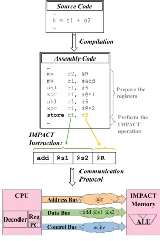
We propose, in this Section, a possible solution to built the proposed IMPACT instruction codes from the instruction set architecture (ISA) of a given processor. The solution consists in using an existing processor ISA without integrating new in-structions or opcodes. In particular, we use the store instruction to monitor the IMPACT operations (arithmetic/logic). The IM-PACT opcode, as well as its operands, will be encoded inside the operands (i.e., registers) of the conventional instruction.
Data Bus add @s1 @s2 @R … mv r2, @R mv r1, #add shl r1, #6 xor r1, #@s1 shl r1, #6 xor r1, #@s2 store r1, r2 … … R = s1 + s2 … Compilation Prepare the registers Perform the IMPACT operation IMPACT Instruction:
Address Bus IMPACT
Memory CPU ALU Decoder Reg PC Control Bus @r add @s1 @s2 write Source Code Assembly Code Communication Protocol
Fig. 8. Implementation of IMPACT Store Instruction.
In Fig. 8, we provide, for an IMPACT addition operation, the compilation process to create the corresponding IMPACT assembly code. First, the compiler generates instructions that encodes the addresses of the IMPACT opcode as well as the operands inside specific registers. These instructions will be transferred via the system buses respecting the conven-tional communication protocol. Then, the compiler generates the store instruction with the previously assembled specific registers. This store instruction is then transferred to the
memory through the system buses respecting the IMPACT communication protocol defined in Subsection IV-C.
The advantage of this solution consists in its facility to be compatible with the processor ISA (no problem in case of version changes). However, the compilation process will be quite complex since it requires to generate a prelimi-nary list of instructions needed then to generate IMPACT instruction using the store instruction. Further solutions to integrate the proposed IMPACT memory instruction code in the ISA are possible. However, they require to change the processor ISA by integrating one or more new instructions (e.g., ’IMPACTAdd’). The compilation process will be then simpler since it does not require to generate the preliminary list of instructions. However, this solution could have some problems of compatibility with future ISA versions.
VI. CONCLUSION
This paper discusses the integration of the In-Memory Computing capabilities into a system composed of a processor and a memory without changing the processor implementation and instruction set. This is acheived by inverting the von Neuman model: instead of reading instructions from memory, the CPU communicates the instructions, in certain formats, to the IMPACT memory via the standard SRAM buses.
The proposed approch allows to benefit from the huge speedup in terms of execution time and energy consumption offered by the IMPACT system, but also to easily interweave conventional CPU instructions and memory computing in-structions. One main advantage of this approach is to have a similar data layout view on both CPU and IMPACT side. Whereas, other conventional approaches (e.g., GPUs) need to copy data and change the layout at run-time.
As future works, we aim to continue characterizing applica-tions on high level, and to develop the compiler for this system. High level optimizations of classical programming languages or new programming paradigms are also under investigation.
REFERENCES
[1] K. C. Akyel, H.-P. Charles, J. Mottin, B. Giraud, G. Suraci, S. Thuries, and J.-P. Noel, “DRC 2: Dynamically Reconfigurable Computing Circuit based on memory architecture,” in IEEE International Conference on Rebooting Computing (ICRC), pp. 1–8, 2016.
[2] M. Kooli, H.-P. Charles, C. Touzet, B. Giraud, and J.-P. Noel, “Software Platform Dedicated for In-Memory Computing Circuit Evaluation,” in IEEE/ACM International Symposium on Rapid System Prototyping (RSP), 2017.
[3] M. Gokhale, B. Holmes, and K. Iobst, “Processing in memory: The Terasys massively parallel PIM array,” Computer, vol. 28, no. 4, pp. 23– 31, 1995.
[4] S. H. Pugsley, J. Jestes, H. Zhang, R. Balasubramonian, V. Srinivasan, A. Buyuktosunoglu, A. Davis, and F. Li, “NDC: Analyzing the impact of 3D-stacked memory + logic devices on mapreduce workloads,” in IEEE International Symposium on Performance Analysis of Systems and Software (ISPASS), pp. 190–200, 2014.
[5] “UPMEM.” www.upmem.com/.
[6] S. Matsunaga, J. Hayakawa, S. Ikeda, K. Miura, T. Endoh, H. Ohno, and T. Hanyu, “MTJ-based nonvolatile logic-in-memory circuit, future prospects and issues,” in Proceedings of the Conference on Design, Automation and Test in Europe, pp. 433–435, 2009.
[7] S. Jeloka, N. B. Akesh, D. Sylvester, and D. Blaauw, “A 28 nm configurable memory (TCAM/BCAM/SRAM) using push-rule 6T bit cell enabling logic-in-memory,” IEEE Journal of Solid-State Circuits, vol. 51, no. 4, pp. 1009–1021, 2016.
[8] Y. Zhang, L. Xu, K. Yang, Q. Dong, S. Jeloka, D. Blaauw, and D. Sylvester, “Recryptor: A reconfigurable in-memory cryptographic Cortex-M0 processor for IoT,” in IEEE Symposium on VLSI Circuits, pp. C264–C265, 2017.
[9] S. Aga, S. Jeloka, A. Subramaniyan, S. Narayanasamy, D. Blaauw, and R. Das, “Compute caches,” in IEEE International Symposium on High Performance Computer Architecture (HPCA), pp. 481–492, 2017. [10] Y. Wang, L. Ni, C.-H. Chang, and H. Yu, “DW-AES: A Domain-Wall
Nanowire-Based AES for High Throughput and Energy-Efficient Data Encryption in Non-Volatile Memory,” IEEE Transactions on Information Forensics and Security, vol. 11, no. 11, pp. 2426–2440, 2016. [11] S. Li, C. Xu, Q. Zou, J. Zhao, Y. Lu, and Y. Xie, “Pinatubo: A
processing-in-memory architecture for bulk bitwise operations in emerg-ing non-volatile memories,” in Design Automation Conference (DAC), 2016 53nd ACM/EDAC/IEEE, pp. 1–6, IEEE, 2016.
[12] F. Vahid and T. Givargis, Embedded system design: a unified hard-ware/software introduction. New York: Wiley, 2002.
[13] I. C. S. S. Committee, “Ieee standard microcomputer system bus,” Institute of Electrical and Electronics Engineers, 1983.
[14] L. Null, J. Lobur, et al., The essentials of computer organization and architecture. Jones & Bartlett Publishers, 2014.