HAL Id: hal-01005817
https://hal.archives-ouvertes.fr/hal-01005817
Preprint submitted on 13 Jun 2014
HAL is a multi-disciplinary open access
archive for the deposit and dissemination of
sci-entific research documents, whether they are
pub-lished or not. The documents may come from
teaching and research institutions in France or
abroad, or from public or private research centers.
L’archive ouverte pluridisciplinaire HAL, est
destinée au dépôt et à la diffusion de documents
scientifiques de niveau recherche, publiés ou non,
émanant des établissements d’enseignement et de
recherche français ou étrangers, des laboratoires
publics ou privés.
Photoluminescence of silicon nano-clusters
functionalized microtoroids
Yves Candéla, Jean-Baptiste Jager, R.P. Nalini, Guoping Lin, M. Terrier,
Vincent Calvo, Fabrice Gourbilleau, Jean Hare
To cite this version:
Yves Candéla, Jean-Baptiste Jager, R.P. Nalini, Guoping Lin, M. Terrier, et al.. Photoluminescence
of silicon nano-clusters functionalized microtoroids. 2013. �hal-01005817�
Photoluminescence of silicon
nano-clusters functionalized
microtoroids
Y. Cand´ela1, J.-B. Jager2, R. Pratibha Nalini3, G. L. Lin1, M. Terrier2, V. Calvo2, F. Gourbilleau3and J. Hare1
1Laboratoire Kastler Brossel, ENS, UPMC, CNRS ; 24 rue Lhomond, 75005 Paris, France 2CEA Grenoble INAC/SP2M/SINAPS Minatec, 17 rue des Martyrs, 38000 Grenoble, France
3CIMAP, CNRS/CEA/Ensicaen/UCBN, 6 Bld Marchal Juin, 14050 Caen, France
jean.hare@lkb.ens.fr
Abstract: We report on the first realization of on-chip toroid microcavities embedding size-controlled silicon nanoclusters (Si-nc), produced by reac-tive magnetron co-sputtering. We demonstrate functionalized whispering gallery microresonators with low volume and high quality factor. Emission properties are optimized by tailoring the size and the shape of the toroids and the Si-nc distribution. Coalescence of Si-nc during the melting of the toroid is minimized by the design of the microdisk preforms. Photolumines-cence in the whispering gallery modes of 13.5 µm diameter microtoroids, is observed in both near-field and far-field.
© 2013 Optical Society of America
OCIS codes: (140.3945) Microcavities; (160.4236) Nanomaterials; (060.2280) Fiber design and fabrication; (300.6280) Spectroscopy, fluorescence and luminescence; (350.3950) Micro-optics
References and links
1. L. Canham, “Silicon quantum wire array fabrication by electrochemical and chemical dissolution of wafers,” Appl. Phys. Lett. 57, 1046–1048 (1990).
2. L. Brus, “Luminescence of silicon materials: Chains, sheets, nanocrystals, nanowires, microcrystals, and porous silicon,” J. Phys. Chem. 98, 3575–3581 (1994).
3. D. Kovalev, H. Heckler, M. Ben-Chorin, G. Polisski, M. Schwartzkopff, and F. Koch, “Breakdown of the k-conservation rule in Si nanocrystals,” Phys. Rev. Lett. 81, 2803–2806 (1998).
4. M. Wolkin, J. Jorne, P. Fauchet, G. Allan, and C. Delerue, “Electronic states and luminescence in porous silicon quantum dots: the role of oxygen,” Phys. Rev. Lett. 82, 197–200 (1999).
5. L. Pavesi, L. Dal Negro, C. Mazzoleni, G. Franz`o, and F. Priolo, “Optical gain in silicon nanocrystals,” Nature 408, 440–444 (2000).
6. M. Dovrat, Y. Goshen, J. Jedrzejewski, I. Balberg, and A. Sa’ar, “Radiative versus nonradiative decay processes in silicon nanocrystals probed by time-resolved photoluminescence spectroscopy,” Phys. Rev. B 69, 155311 (2004). 7. I. Sychugov, R. Juhasz, J. Valenta, and J. Linnros, “Narrow luminescence linewidth of a silicon quantum dot,”
Phys. Rev. Lett. 94, 87405 (2005).
8. V. Sandoghdar, F. Treussart, J. Hare, V. Lef`evre-Seguin, J.-M. Raimond, and S. Haroche, “Very low threshold whispering-gallery mode microsphere laser,” Phys. Rev. A 54, R1777 (1996).
9. T. J. Kippenberg, S. Spillane, and K. J. Vahala, “Kerr-nonlinearity optical parametric oscillation in an ultrahigh-q toroid microcavity,” Phys. Rev. Lett. 93, 083904–4 (2004).
10. R. K. Chang and A. J. Campillo, eds., Optical processes in microcavities, vol. 3 of Advanced Series in Applied Physics(World Scientific, 1996).
11. D. K. Armani, T. J. Kippenberg, S. M. Spillane, and K. J. Vahala, “Ultra-high-Q toroid microcavity on a chip,” Nature 421, 925–928 (2003).
12. J. Verbert, F. Mazen, T. Charvolin, E. Picard, V. Calvo, P. No´e, J. M. G´erard, and E. Hadji, “Efficient coupling of Er-doped silicon-rich oxide to microdisk whispering gallery modes,” Appl. Phys. Lett. 86, 111117–1–111117–3 (2005).
13. J. Verbert, F. Mazen, T. Charvolin, E. Picard, V. Calvo, P. No´e, J. G´erard, E. Hadji, F. Orucevic, J. Hare, and V. Lef`evre-Seguin, “Room temperature emission from er-doped silicon-rich oxide microtorus,” Eur. Phys.J. Appl. Phys 34, 81–84 (2006).
14. J. Kalkman, A. Tchebotareva, A. Polman, T. J. Kippenberg, B. Min, and K. J. Vahala, “Fabrication and charac-terization of erbium-doped toroidal microcavity lasers,” J. Appl. Phys. 99, 083103 (2006).
15. F. Gourbilleau, X. Portier, C. Ternon, P. Voivenel, R. Madelon, and R. Rizk, “Si-rich/SiO nanostructured multi-layers by reactive magnetron sputtering,” Appl. Phys. Lett. 78, 3058 (2001).
16. M. Zacharias, J. Heitmann, R. Scholz, U. Kahler, M. Schmidt, and J. Bl¨asing, “Size-controlled highly luminescent silicon nanocrystals: A SiO/SiO2superlattice approach,” Appl. Phys. Lett. 80, 661 (2002).
17. A. Belarouci and F. Gourbilleau, “Microcavity enhanced spontaneous emission from silicon nanocrystals,” J. Appl. Phys. 101, 073108 (2007).
18. R.-J. Zhang, S.-Y. Seo, A. P. Milenin, M. Zacharias, and U. G¨osele, “Visible range whispering-gallery mode in microdisk array based on size-controlled Si nanocrystals,” Appl. Phys. Lett. 88, 153120 (2006).
19. G. Lin, B. Qian, F. Oruˇcevi´c, Y. Candela, J. Jager, Z. Cai, V. Lef`evre-Seguin, and J. Hare, “Excitation mapping of whispering gallery modes in silica microcavities,” Opt. Lett. 35, 583–585 (2010).
20. F. Orucevic, V. Lef`evre-Seguin, and J. Hare, “Transmittance and near-field characterization of sub-wavelength tapered optical fibers,” Opt. Lett. 15, 13624–13629 (2007).
21. B. Redding, E. Marchena, T. Creazzo, S. Shi, and D. Prather, “Comparison of raised-microdisk whispering-gallery-mode characterization techniques,” Opt. Lett. 35, 998–1000 (2010).
22. K. Srinivasan, A. Stintz, S. Krishna, and O. Painter, “Photoluminescence measurements of quantum-dot-containing semiconductor microdisk resonators using optical fiber taper waveguides,” Phys. Rev. B 72, 205318 (2005).
23. R. Kekatpure and M. Brongersma, “Fundamental photophysics and optical loss processes in Si-nanocrystal-doped microdisk resonators,” Phys. Rev. A 78, 23829 (2008).
24. M. Ghulinyan, D. Navarro-Urrios, A. Pitanti, A. Lui, G. Pucker, and L. Pavesi, “Whispering-gallery modes and light emission from a silicon-nanocrystal-based single microdisk resonator,” Opt. Express 16, 13218–13224 (2008).
1. Introduction
Due to its indirect band-gap, Silicon was for a long time considered as a poor light emitter. The discovery in the 90’s of an efficient emission from porous Si produced by electrochemistry [1] or nanostructured Si obtained by other methods [2] led to lively interest [3, 4]. It was early recognized that nanometer scale confinement results in a weakening of the indirect bandgap properties. Active researches yield to evidence of optical gain in Silicon nanocrystals [5]. This increased the activity [6, 7] in silicon photonics because an on-chip a Si laser would be a major achievement towards CMOS compatible photonics, but direct laser action has not yet been achieved.
In this quest, a critical point is the choice of high-performance cavities which can be com-bined with this active material. In this perspective, the Whispering Gallery Modes (WGM) of fused silica microcavities, exhibiting ultra high-Q up to 1010and small mode volumes V down to 100λ3constitute an appealing option. The high Q/V figures of merit achieved in these
cav-ities have allowed to observe low-threshold lasers [8], nonlinearcav-ities [9] and quantum effects [10]. The on-chip microtoroids introduced in [11] are peculiarly suited in the perspective of thin-film based all-silicon devices.
Silicon nanoclusters (Si-nc) are usually obtained from sub-stoichiometric silica, generally called “silicon-rich silicon oxide” (SRSO). Thermal annealing then enables phase segregation of the excess silicon and Si-nc nucleation. SRSO itself is obtained by different methods includ-ing laser pyrolysis [4], chemical vapor deposition [5], electron beam evaporation [12, 13] and ionic implantation [14].
An interesting variant is the reactive co-magnetron sputtering technique [15, 16]. This pro-cess not only produces SRSO, but also enables the production of multilayers (ML) consisting in an alternation of SiO2and SRSO films, and allows to accurately define the SRSO sublayer
thickness. As the growth of Si-nc during the annealing step is constrained by the SRSO sub-layer, this method allows to take control on their size distribution and on the resulting emission bandwidth. This unique property makes this technique very appealing for optical applications where size monodispersity could be a decisive advantage.
To the best of our knowledge, two papers have been devoted to Si-nc ML functionalized microcavities : planar microcavities in [17] and WGM microdisks in [18]. In this paper, we report for the first time on the combination of very-high quality factor WGM microtoroids with size controlled Si-nc produced by magnetron sputtering. We have successfully fabricated ML SRSO microdisks, and converted them to Si-nc doped microtoroids by laser fusion. We have then demonstrated an efficient coupling of the Si-nc emission with low order WGM of the microcavities. The obtained photoluminescence (PL) signal and its limiting factors will be presented and analyzed.
2. Sample fabrication
The production of microtoroids relies on several steps, the first of which consist in the fabrica-tion of a silica microdisk on a silicon pedestal. The processing steps used for this purpose are described elsewhere [11]. In brief, starting from an oxidized silicon substrate, lithography fol-lowed by wet etching in HF leads to silica disks on silicon, and then dry etching of the silicon creates the pedestals, isolating the disks from the silicon surface.
Fig. 1. (a) Transmission electron microscope image of a typical SRSO ML sample obtained with reactive co-magnetron sputtering technique, followed by thermal annealing at 1050°C for 1h. The white lines underline the boundaries of the MLs. In the inset, a zoom on a Si-nc shows the crystalline planes (b) Emission spectra of silicon nano-clusters functional-ized microdisks pumped at 532 nm (c) Schematic of a functionalfunctional-ized silica microdisk on a silicon pedestal.
2.1. SRSO microdisks
The active material consists of successive layers of pure and sub-stoichiometric silica deposited by reactive magnetron co-sputtering [15]. This technique uses two targets of Si and SiO2in an
Ar − H2plasma. The injection of H2in the vacuum chamber allows the reduction of the SiO2
target to favor a higher Si incorporation. During deposition the substrate temperature is set to 500°C and the chamber pressure is set to 0.4 Pa.
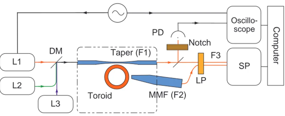
LP MMF (F2) Notch L3 L1 L2 Taper (F1) SP Oscillo-scope Toroid Computer DM PD F3
Fig. 2. Three LaserL1,L2andL3combined on a dichroic beam-splitterDM, are injected in the tapered fiber to characterize or to pump the microtoroid. The taper (F1) output signal is split to either measure the total transmitted power or analyze the PL with spectrometerSP. In both cases the pump is filtered out by using notch or Long pass filter respectively. The far-field (scattered light) is also collected using the thinned multimode fiber MMFF2and analyzed with the same spectrometer.
The SRSO sublayer thickness determines the mean diameter of the Si-nc, hence the central wavelength of the emission, ranging from visible to near infrared for thickness varying from 1 nm to 4 nm. For the purpose of this paper, we focus on SRSO sublayer thickness of 3 nm, leading to a central emission wavelength in the MLs structure of about 775 nm.
The SRSO MLs are deposited on top of a pure silica microdisk. This approach, introduced in [12], avoids the specific difficulty of SRSO wet chemical etching. The supporting silica microdisks have a diameter varying from 20 µm to 50 µm and a thickness ranging from 0.5 to 1.5 µm (see Fig. 1-c).
The samples are subsequently annealed at 1050°C for 1 h under pure N2 atmosphere, in
order to nucleate the Si-nc. Fig. 1-(a) shows a typical image of the material after annealing. In Fig. 1-(b) is plotted the emission spectrum of a microdisk embedding Si-nc, optically pumped at 532 nm.
2.2. Functionalized microtoroids
The deposited microdisks are then fused close to the focus of a CO2laser Gaussian beam, with
a waist of 110 µm. We used a circular polarization in order to keep a cylindrical symmetry. The silicon pedestal acting as an efficient heat sink, only the disk border reaches the fusion temperature, and surface tension shapes the molten material into a toroid.
As the melting temperature of silicon is lower than that of SiO2, the embedded Si-nc can be
damaged by the laser fusion. In order to minimize this effect, the microdisks are molten with a laser power as small as possible. This melting threshold was determined by fusing identical microdisks with different powers. It was found about 10 kW/cm2, thought dependent on the
microdisk geometry.
The microtoroid shape was characterized with a scanning electronic microscope (SEM) and an atomic force microscope. The observed surface roughness is under detection limit, with an amplitude below 1 nm, for 1 µm2scan.
3. Experiment
The experimental setup is shown in Fig. 2. As in [19], the microtoroid is hold on a three axis PZT-actuated translation stage and is coupled to a tapered fiber.
Silica disk (µm) SRSO Toroid (µm) Parameters Td Dd Dp N TSRSO TSiO2 D d
Sample A 1.5 50 7 70 3 nm 15 nm 33 8 Sample B 0.5 20 7 150 3 nm 7 nm 13.5 3
Table 1. Geometrical parameters of the microdisks, multilayers, and resulting microtoroids used in the experiment. Td, Dd and Dp denote the disk thickness, diameter and pedestal
diameter, respectively. N, TSRSOand TSiO2 denote the number of bilayers, SRSO thickness and Silica thickness, respectively. D and d are the outer and minor diameters of the toroid.
Three different lasers are alternatively or simultaneously used. The first one (L1) is a tunable extended-cavity laser diode (ECLD) atλ1=775 nm, which is used to characterize the cold cavity spectrum next to the maximum of emission. The two others, used as pump lasers, are a frequency-doubled Nd3+:YAG providing 25 mW atλ2=532 nm (L2) on one hand and a single mode tunable ECLD atλ3=405 nm with a power of 13 mW (L3) on the other hand. The L2/L3 can be combined with L1 using a dichroic mirror and coupled to the same taper for evanescent coupling to the microtoroid.
With a coupling gap of ∼ 0.5 µm the intrinsic microcavity losses dominate the coupling losses. When scanning L1 frequency one detects the resonances in the vicinity of 775 nm as absorption dips on the transmitted power, monitored on photodiode PD (as plotted in Fig. 4). This provides the microtoroid quality factor Qeat emission wavelength. In the same way, the
tunable laser L3 can be used to characterize the WGM spectrum in the absorption range, and estimate the quality factor Qp.
The light emitted into the WGM by the Si-nc is detected in two ways. On the one hand, it is evanescently coupled out by the taper and led to the output fiber F1 (near-field signal). On the other hand, it is scattered in the toroid and collected through a thinned multimode fiber F2 (far-field signal) like in [20, 21, 22]. At the output of both fibers the pump is removed by using a long pass filter LP (OG590). The two signals are then analyzed by an imaging spectrograph with a f = 300 mm focal length.
In these experiments a challenging difficulty lies in the strong infrared (IR) PL induced in the fibers by the short wavelength lasers used to pump the Si-nc. In many cases this spurious IR PL hides the interesting signal in both F1 and F2. This problem originates in the composition of the fiber used in the experiment. Our tapers are usually produced with IR single mode fibers (SMF) which have pure silica cladding and doped core: the deleterious signal comes from the doping elements. In contrast, the SMF adapted to short wavelength have a silica core and doped cladding, which makes them unsuitable for taper fabrication. When using blue laser L3, this spurious PL is significantly stronger than with L2. Therefore we abandoned resonant intracavity pumping with L3 and decided to use the non-tunable green laser L2.
The usual tapers, made from IR-fiber SMF 125-A-42, are single-mode at Si-nc emission wavelength. However, at the pump wavelengthλ2, they are multimode. The corresponding low
effective index could excite poorly confined higher order WGM. Nevertheless, this effect is minimized by injecting L2 into the taper through a SMF. Finally, the rather high power of this laser allows to efficiently pump the Si-nc located in the fundamental mode.
In the last stage of the experiment, the taper fabrication was improved in a decisive way to eliminate this fiber core PL limitation. This consisted in fabricating an “hybrid” taper made from two different fibers. A small length ∼ 15 mm of pure silica cladding SMF was spliced, on both sides, with pure silica core fibers (3M FS-SN-3224) suitable for visible light operation. This combination allows to minimize the fiber PL while preserving the ability to produce a good quality taper, with a transmittance T ≥ 90% atλ1=775 nm.
Fig. 3. SEM images of microtoroids cut with FIB. (a) Sample A general view, (b) zoom on the roll of sample A. Inset (e) : toroid similar to sample A, selected for the visibility of the coalesced Si clusters. (c) Sample B general view, (d) zoom on the roll of sample B toroid. On (d) and (e) the dashed line shows the boundary between silica and deposited material.
4. Results
We present successively the results obtained with two samples A and B of different thickness and diameters. Their geometrical parameters are summarized in table 1. Sample A was pro-duced in a first stage of the experiment, and the analysis of its characteristics led to engineer sample B, which features the main results of this work. For both samples, after annealing, the emission wavelength band, spanning from 730 nm to 830 nm, corresponds to a distribution of Si-nc diameters centered at 3 nm with a dispersion estimated to 0.3 nm.
We first used pure silica microdisks presenting a moderate thickness and a large distance between the pedestal and the edge (sample A in Table 1). The resulting microtoroid exhibit fundamental TE modes with quality factors Qe=2 × 10⁷and Qp=106. For all other observed
modes (10 per FSR), Qeis reduced to about 4 × 10⁶. In spite of these good quality factors, the
Si-nc emission was to weak to be isolated from the spurious fiber emission in F1.
An explanation of this small emission eficiency is provided by a structural analysis. After the optical characterization, the toroid was cut using a focused ion beam (FIB) in order to study the silicon distribution after melting. SEM images of the section are shown in Fig. 3-(a) and (b). These pictures evidence the usual rolled-up shape of the toroid originating from the large pedestal–edge distance [14]. Moreover, at high resolution, one observes a spiral shaped distribution of structures with a typical diameter of about 100 nm, which result from Si-nc coalescence, as confirmed by an energy dispersive X-ray spectrometry measurement, to be
Taper (F1) MMF (F2) 600 700 800 6 2 0 4 0.4 0.2 0 800 700 600 Emission wavelength (nm)
Raw emission spectra (10
3 /s)
(a)
(b)
(d)
1.0 0.9 0.8 80 60 40 20 0 15GHz(c)
Taper transmission Frequency shift (GHz) Q = 25,000Fig. 4.(a) Top view of the experiment. (c) Absorption dip for a fundamental mode observed when scanningL1. (b) Spectrum of the near field signal at output of the hybrid taper. (d) Spectrum of the far field signal in the same conditions. frequency.
published elsewhere. To illustrate this feature we show in the inset (e) of Fig. 3 the cross section of a toroid very similar to that of sample A, but with a much higher contrast. One actually observes the mid-size nanostructures created by coalescence of Si-nc, favored by advection during the melting. One also distinguishes the pure silica bottom layer of the microdisk, and above it a silicon doped layer.
If some nanometer sized Si-nc survived the melting process, their spatial distribution must basically be the same as for the larger visible ones. Due to the roll-up shape, the depth of the active region matches the 1.5 µm thickness of the supporting microdisk, while the radial extension of the fundamental mode is about 2λ1 below the surface. This results in a nearly
vanishing coupling between the emitting Si-nc and high-Q WGM, and explains the dim signal. Achieving a better coupling, requires a thinner silica substrate and a better control of the toroid shape. For this purpose, the fabrication process is modified with 3 times thinner support-ing silica microdisks and a 3 times smaller distance pedestal–edge, as described for sample B in Table 1. We keep the same pedestal diameter, and the same total disk thickness by increas-ing by a factor 4 the number of SRSO layers, with a reduced spacincreas-ing to improve the Si-nc concentration. In what follows we focus on this improved sample.
Fig. 3-(c) displays SEM images of the cross section of this toroid, demonstrating that is not rolled up. Actually, decreasing the amount of fused material inhibits the large displacement associated to the usual roll-up shape, and results in a 3 times smaller minor diameter. On the zoom presented in Fig. 3-(d) there is no indication of coalescence : in contrast to (b) and (e) the observable nanostructures have a much smaller apparent size. We observe no sign of advection, as the preserved Si-nc are almost homogeneously spread in the whole section.
Putting in contact the hybrid taper with the microtoroid allows to maximize the output cou-pling. The resulting signals, simultaneously collected by using the two fibers F1 and F2, are
4 3 2 1 0 760 750 740 730 720 Emission wavelength (nm) PL intensity (10 3/s)
Fig. 5.Same as Fig. 4-(b) but acquired at higher resolution and after subtraction of the fiber PL background.
analyzed with SP using a 300 grooves/mm grating (resolution ≈ 1 nm). In Fig. 4, we have plotted the corresponding spectra. Fig. 4-(a) is a picture of the experiment clarifying the two output ports F1 and F2, and Fig. 4-(c) is the absorption dip observed when scanning L1 in undercoupled conditions, exhibiting a reduced albeit still large Qe in sample B. Fig. 4-(b) is
the “near-field” signal detected at the hybrid taper output. The emission into the WGM with its characteristic quasi-periodicity (FSR ≈ 9 nm) is clearly observed. This spectrum is super-imposed on a large background, which results from the PL created in the central part of the taper and in the auxiliary multimode fibre F3 leading to SP. Only the PL emitted in the WGM is coupled back to the taper, therefore the broadband component of Si-nc emission does not contribute to this background.
Fig. 4-(d) shows the “far-field” signal coming from the MMF F2, in the same conditions. As a fraction of the scattered pump is collected by F2, it generates a large spurious PL which is the dominant contribution of the background. Thanks to the scattering losses of the micro-toroid, the Si-nc emission structured by the WGM is still present, but with a reduced contrast. A comparison between (b) and (d) demonstrates that the taper coupling has a better extraction efficiency than the omnidirectional scattering: in spite of a larger background, it enables a 20 times better detection efficiency of the WGM.
When working in non-contact conditions we recover the high quality factor of the WGM. The F1 signal spectrum is recorded in SP, with a 1,200 grooves/mm grating enabling a higher reso-lution. The pump-induced fibre PL background was first recorded with a large gap (g ∼ 10 µm), in order to digitally remove it from the detected signal. In Fig. 5 is plotted the resulting spec-trum obtained by this procedure. One recognizes the 9.0 nm periodicity of the WGM specspec-trum and 4 modes in each FSR. The observed linewidth of about 0.5 nm is here instrumental-limited. The two strongest peaks in a given FSR are separated by about 4.5 nm, compatible with the TE-TM shift expected for this small microtoroid.
5. Conclusion
We have for the first time produced on-chip silica toroidal microcavities embedding Si-nc of controlled size, and have investigated their photoluminescence. This combination of the best material with the highest Q/V silicon based microcavities was achieved by the reactive
mag-netron sputtering of SRSO on silica microdisks, followed by laser reflow and surface tension reshaping. These active cavities feature a Q-factor larger by one order of magnitude than the one obtained for microdisks in [23, 24], and is mostly limited by diffraction and not by scattering.
The optical characterization of the functionalized cavities has been realized in both the near-field (evanescently coupled taper) and the far-near-field (scattering collected by a fiber tip). It shows that rather large toroids, due to their “rolled-up” shape, maximize the quality factor, but gives a geometric mismatch between the emitters distribution and the WGM field, resulting in a very weak emission. In contrast, significantly smaller toroids, presenting an optimized symmetric shape, at the expanse of a significantly reduced Q-factor, feature a good coupling of the Si-nc to the WGM and give rise to a well resolved WGM emission.
The technical limitation coming from the spurious photoluminescence of the fibers was over-come by the realization of an hybrid taper. A further improvement in the taper fabrication technique is required to enable a better coupling of the pump in a resonant WGM. Such a con-figuration providing a much higher sensitivity would allow a better material optimization and the investigation of the fundamental loss mechanisms in Si-nc.
6. Acknowledgment
This work has been supported by the Region le-de-France in the framework of C’Nano IdF, the nanoscience competence center of Paris Region. Y. C. acknowledges support granted by the French Ministry of Higher Education and Research.