HAL Id: hal-01745644
https://hal.archives-ouvertes.fr/hal-01745644
Submitted on 28 Mar 2018
HAL is a multi-disciplinary open access
archive for the deposit and dissemination of
sci-entific research documents, whether they are
pub-lished or not. The documents may come from
teaching and research institutions in France or
abroad, or from public or private research centers.
L’archive ouverte pluridisciplinaire HAL, est
destinée au dépôt et à la diffusion de documents
scientifiques de niveau recherche, publiés ou non,
émanant des établissements d’enseignement et de
recherche français ou étrangers, des laboratoires
publics ou privés.
Design challenges for prototypical and emerging memory
concepts relying on resistance switching
Christophe Muller, D. Deleruyelle, O. Ginez, Jean-Michel Portal, Marc
Bocquet
To cite this version:
Christophe Muller, D. Deleruyelle, O. Ginez, Jean-Michel Portal, Marc Bocquet.
Design
chal-lenges for prototypical and emerging memory concepts relying on resistance switching. 2011 IEEE
Custom Integrated Circuits Conference (CICC 2011), Sep 2011, San Jose, CA, United States.
�10.1109/CICC.2011.6055316�. �hal-01745644�
Design Challenges for Prototypical and Emerging
Memory Concepts Relying on Resistance Switching
Ch. Muller, D. Deleruyelle, O. Ginez, J-M. Portal, and M. Bocquet
IM2NP, UMR CNRS 6242, Aix-Marseille Université, 13451 Marseille Cedex 20, France e-mail: [email protected]
Abstract—Integration of functional materials in memory
archi-tectures led to emerging concepts with disruptive performances as compared to conventional charge storage technologies. Be-side floating gate solutions such as EEPROM and Flash, these alternative devices involve voltage or current-controlled switching mechanisms between two distinct resistance states. The origin of the resistance change straightforwardly depends upon the nature and fundamental physical properties of func-tional materials integrated in the memory cell. After a general overview of non volatile memories, this paper is focused on prototypical and emerging memory cells and on their ability to withstand a downscaling of their critical dimensions. In addi-tion, despite different maturity levels, a peculiar attention is turned toward common guidelines helpful for designing em-bedded or distributed resistive switching memory circuits.
Keywords—Prototypical and emerging memory concepts; re-sistance switching; operation mechanisms; memory design; embedded or distributed memory circuits.
I. OVERVIEW
Currently, the microelectronic industry is facing new technological challenges for continuously improving per-formances of memory devices in terms of access time, stor-age density, endurance or power consumption. The major bottleneck to overcome is the downsizing of memory cell dimensions necessary to integrate a larger number of ele-mentary devices and subsequently more functionalities on a constant silicon surface. This drastic size reduction is con-strained, in particular, by the intrinsic physical limits of materials integrated in the memory architecture.
Beside volatile random access memories (RAM) such as Dynamic (DRAM) or Static (SRAM), non volatile memory technologies may be subdivided in two categories depend-ing upon the mechanism used to store binary data. A first group of solid state devices is based on charge storage in a polysilicon floating gate. In this family, gathering usual EEPROM and Flash technologies [1], new concepts or ar-chitectures are required to satisfy CMOS “More Moore” scaling trends. For instance, Si1–xGex “strained silicon”
technology enables boosting the charge carrier mobility and discrete charge trapping improves data retention and enables an extension towards “multi-bits” storage. Presently, Flash technology still remains the undisputed reference, regardless of its NAND (dense and cheap) or NOR (fast) architecture. However, as the scaling of the conventional floating gate
cell becomes ever more complicated below 32 nm node, opportunities for alternative concepts are rising. In the last two decades, several major semiconductor Companies have explored new solutions integrating a functional material, whose fundamental physical property enables data storage.
Older technology, called FRAM for Ferroelectric RAM [2], is in small volume production for several years by Fujit-su and Texas Instruments which license Ramtron patents. With their DRAM-like architecture FRAM memories inte-grate ferroelectric capacitors that permanently store electri-cal charges. Thanks to their low voltage operations, fast access time and low power consumption, FRAM devices mainly address “niche” applications such as contactless smart cards, RFID tags and nomad devices.
Excluding FRAM technology, recent R&D efforts also led to a new class of disruptive technologies based on resis-tive switching mechanisms. These memories, presenting two stable resistance states controlled by an external current or voltage, attract much attention for future solid state de-vices. The physical origin of the resistance change depends upon the nature and fundamental physical property of mate-rials integrated in the memory cell. As a result, a broad panel of new concepts is currently rising: magnetoresistive memories (MRAM) and derived concepts; phase change memories (PCM); resistive memories (RRAM) including oxide resistive (OxRRAM) and “nanoionic” memories (CBRAM and PMC) [3]. As compared to other technolo-gies, PCM and RRAM memories are more favourably posi-tioned as alternatives to Flash for sub-22 nm nodes. Never-theless, these two technologies have different maturity lev-els: while first PCM products are available (e.g. OmneoTM
by Micron, former Numonyx), RRAM memories are still at early R&D stage. Following 2010 ITRS’s report, MRAM, PCM and FRAM are categorized as “prototypical” memo-ries whereas RRAM is an “emerging” memory [4].
Hence, alternative non volatile memory concepts, either evolutionary or revolutionary, are being explored to satisfy the need for higher storage capacity and better performanc-es. Within a broad panel of innovative solutions, this review specifically addresses resistive switching technologies. After a brief description of memory cells and their ability to withstand downscaling of their critical dimensions, peculiar attention is turned toward common guidelines helpful for designing embedded or distributed memory circuits.
II. MEMORY MARKETS FOR RESISTIVE TECHNOLOGIES
To penetrate the markets currently covered by SRAM, DRAM and Flash memories, prototypical and emerging concepts are facing stringent requirements of process com-patibility and scalability at material, device and circuit lev-els. Status and outlook may be proposed as follows:
MRAM arising from spintronics may be viewed as a credible candidate to replace existing technologies in many applications requiring standalone or embedded so-lutions combining Flash-like non volatility, SRAM-like fast nanosecond switching and DRAM-like infinite en-durance. For future, “Spin Torque Transfer” (STT-MRAM) concept appears as a promising technology able to merge aforementioned advantages and scalable for aggressive technological nodes (cf. §III).
PCM is probably the most advanced alternative memory concept in terms of process maturity, storage capacity and access time. Furthermore, the phase change memory element exhibits an excellent ability to withstand a downsizing of its critical dimensions. Considering limi-tations in terms of high reset current and low perfor-mances in retention, PCM is rather positioned as a NOR Flash substitute. Nevertheless, it may be also envisaged to rethink PCM subsystem architecture to bring the tech-nology within competitive range of DRAM. To exploit PCM’s scalability as a DRAM alternative, new design solutions are expected to balance long latencies, high energy writing and finite endurance [5].
RRAM concept is in an earlier stage of development compared with MRAM and PCM. Since RRAM memory elements can be integrated into Back-End Of Line (BEOL), this technology is of particular interest for high density storage with possibly multi-levels three-dimensional architectures. Metal-organic complex-based RRAM [6], transition metal oxide (TMO) based Ox-RRAM [7,8] and chalcogenide-based CBRAM appear as promising candidates [9]. However, retention and endur-ance still remain to be demonstrated for CBRAM devic-es, while the high reset current is an issue in TMO-based memory devices. As a consequence, RRAM concepts, still in their infancy, require further academic and indus-trial investigations (i) to validate integration and scala-bility capabilities; (ii) to uncover the physical origin of resistance switching which remains sometimes contro-versial; (iii) to model the reliability.
Figure 1. Circuit/architecture of non volatile systems: (a) Conventional implementation with logic block and standalone non volatile memory (NVM) on separated chips. This configuration enables integrating separate-ly optimized technologies but requires tradeoffs in terms of cost and com-munication speed between chips. (b) Embedded implementation with NVM and logic block on a single monolithic substrate. (c) Implementation with distributed NVM circuits on a single chip.
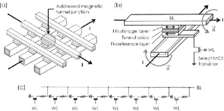
Figure 2. (a) To write MRAM bit, currents are passing through perpen-dicular metal lines surrounding MTJ. (b) The resultant magnetic fields enable programming a bit in reversing magnetization of upper FM storage layer (select MOS transistor is OFF). To read a bit, a current is passing through the MTJ and its resistance is sensed (select MOS transistor is ON). (c) Schematic diagram of series-parallel architecture for 1T/1MTJ cells.
Beside conventional standalone (Fig. 1a) and embedded (Fig. 1b) memories, emerging resistive concepts also enable designing innovative electronic functions such as field pro-grammable gate array (FPGA) or logic devices (e.g. Flip Flop) in which non volatile memory circuits are distributed over a single chip (Fig. 1c). This latter distributed imple-mentation requires CMOS compatible, low cost, low voltage and low power non volatile memory elements.
Before investigating novel architectures, it is of primary importance to develop design kits compatible with microe-lectronics design suites like Cadence or Mentor. Design kits dedicated to memories require first compact models describ-ing cell’s properties and verification tools that enable de-signing and checking the circuit layout [3].
III. MAGNETORESISTIVE MEMORIES, MRAM
In magnetoresistive devices, data are no longer stored by electrical charges, as in semiconductor-based memories, but by a resistance change of a complex magnetic nanostructure [10]. MRAM cells integrate a magnetic tunnel junction (MTJ) consisting of a thin insulating barrier (i.e. tunnel oxide) separating two ferromagnetic (FM) layers. Using lithographic processes, junctions are etched in the form of sub-micron sized pillars connected to electrodes. In conven-tional FIMS (Field Induced Magnetic Switching), each MTJ is located at the intersection of two perpendicular metal lines (Fig. 2a). MTJ resistance depends upon the relative orientation of magnetizations in the two FM layers: the magnetization in FM reference layer is fixed whereas the one in FM storage layer is switchable (Fig. 2b). Magnetiza-tion reversal in FM storage layer is controlled by two exter-nal magnetic fields produced by currents injected in the surrounding metal lines. Tunnel magneto-resistance (TMR) is due to tunnelling of electrons through the thin oxide layer sandwiched between two FM films having either antiparallel (high resistance state “0”) or parallel (low resistance state “1”) magnetizations.
In MRAM technology three major issues are identified: (i) low resistance discrimination between “0” and “1” states (i.e. small sensing margin); (ii) high sensitivity to disturb
during writing (“bit fails”); (iii) high currents (few mA) required for magnetization reversal. To overcome these issues, different solutions are proposed:
To enlarge the sensing margin, the tunnel barrier in amorphous aluminium oxide AlOx of first device
genera-tions was progressively replaced by crystallized magne-sium oxide MgO.
Everspin Company (former Freescale), world’s first volume MRAM supplier, already sells a 4, 8 and 16 Mb MRAM chips based on 180 nm CMOS technology and relying on the “Toggle” concept to limit disturbs during writing [11]. Thanks to a new free layer magnetic nanostructure called “synthetic antiferromagnet” (SAF), an appropriate bit orientation and a current pulse se-quence, MRAM cell bit state is programmed via Savtchenko switching. In that configuration, a single metal line alone cannot switch the bit, providing greatly enhanced selectivity over the conventional FIMS MRAM.
In October 2010, French startup Crocus Technology and TowerJazz completed the first stage integration of “Thermally-Assisted” MRAM into 130 nm CMOS plat-form. In TA-MRAM cell, a current injected in MTJ dur-ing writdur-ing induces a Joule heatdur-ing in FM layers and the subsequent temperature increase facilitates the magneti-zation reversal [12]. TA-MRAM concept enables (i) shrinking the memory cell size with only one metal line to produce magnetic field; (ii) reducing the power con-sumption thanks to limited writing current; (iii) improv-ing bit fails immunity.
More recently, STT (“Spin Torque Transfer”) switching was proposed to solve aforementioned issues and make MRAM memory compatible with more aggressive nodes. Large Companies (e.g. Renesas, Hynix, IBM, Samsung…) and few startups (e.g. Grandis, Avalanche, Everspin, Crocus…) are actively working on this new concept and state they can push the integration limits beyond 45 and 65 nm nodes for standalone and embed-ded memories respectively [13]. In STT writing mode a spin-polarized current, which flows through MTJ, exerts a spin torque on the magnetization of FM storage layer [14]. Technologically, STT concept requires the integra-tion of a polarizer to select the spin of electrons injected into the magnetic nanostructure and ensuring the mag-netization reversal. As compared to conventional MRAM cells, STT-RAM solution is said to consume less power, to improve bit selectivity and to reduce the memory cell size to approximately 6-9 F2.
Similarly to DRAM, EEPROM or NOR Flash memories and whatever the writing mode (Toggle, TA or STT), MRAM core-cell is based on the association of 1 select MOS transistor with 1 magnetic junction (i.e. 1T/1MTJ). To individually access each memory cell, magnetic tunnel junc-tions are located at each intersection of a bottom “Word Line” (WL) connected to the transistor gate and an upper “Bit Line” (BL) (Fig. 2c). In contrast to multi-layer structure
proposed for RRAM technology, such 1T/1MTJ cells disa-ble stacking memory layers due to disturbs between neigh-bouring cells during magnetic field-assisted writing.
Polarization of “Word”, “Bit” and “Source” (SL) lines used to select one core-cell in the memory matrix straight-forwardly depends on the writing mode. In TA-MRAM, writing requires a heating current injection in MTJ obtained in applying a positive voltage on the gate of the select tran-sistor (WL) of the addressed core-cell whereas the source line is grounded. Concomitantly, a current is injected in single metal line (BL) to create a magnetic field that enables switching of FM storage layer. In STT writing mode, a positive voltage is applied on the select transistor gate (WL) of the addressed cell [15]. Since writing does not require magnetic field, only bipolar voltage is applied between BL and SL to inject a top-down or bottom-up spin polarized current enabling magnetization reversal.
Beside memory architectures, TA [16] or STT [17] MTJs may be also integrated in reconfigurable FPGA. Using a heterogeneous design there is no need to load the configura-tion data from an external non volatile memory as required in SRAM-based FPGA. Non volatility enables reducing both power consumption and configuration time required at each start-up of the circuit in comparison with classical static random access memory-based FPGAs.
IV. PHASE CHANGE MEMORIES, PCM
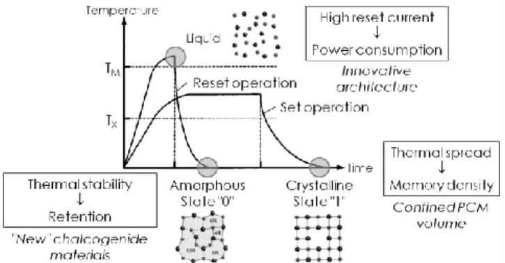
Since the 1970s, chalcogenide phase change materials at-tract much attention for data storage applications [18], par-ticularly in rewriteable optical media such as compact, digi-tal versatile or more recently Blu-ray discs. In addition, they offer a great potential for non volatile phase change memo-ries abbreviated as PCM [19,20]. This concept exploits the resistance change (few orders of magnitude) due to reversi-ble amorphous (state “0”) to crystalline (state “1”) phase transitions. As depicted in Fig. 3, to reach amorphous state (i.e. reset operation), GST material is heated above the melt-ing temperature TM (typically 600-700°C) and then rapidly
cooled. In contrast, GST material is placed in the crystalline state (i.e. set operation) when “slowly” (few tens of ns) cooled from a temperature in between melting point TM and
crystallization temperature TX (Fig. 3).
Figure 3. Temperature profiles used for set and reset operations in PCM. Innovations are mandatory to improve data retention, reduce power
con-sumption and increase memory density.
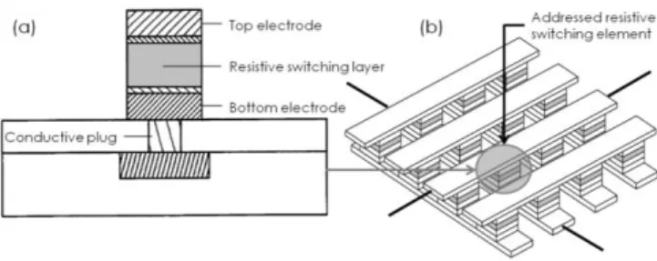
Figure 4. (a) Conventional PCM architecture in which two adjacent memory cells are coupled to a common digit line. Access MOS transistor driven by a word line WL is connected to phase change element through a conductive plug acting as a "heater". (b) 1 access device/1 resistor memory cell. (c) Electrical schematic arrangement of a PCM memory array.
Technologically, a layer of chalcogenide alloy (e.g. Ge2Sb2Te5, GST) is sandwiched between top and bottom
electrodes: the phase change is induced in GST programma-ble volume through an intense local Joule effect caused by a current injected from bottom electrode contact acting as a “heater” (Fig. 4a). As illustrated in Fig. 3, improvement of PCM performances needs to overcome three main issues:
Design innovative cell architectures that enable reducing reset current which remains quite high in existing proto-types (typically 0.5 mA).
Propose new chalcogenide materials exhibiting a higher crystallization temperature to improve data retention (spontaneous amorphous-to-crystalline transition) and crystallizing rapidly to decrease switching time.
Fabricate confined phase change volume to limit heat spread toward neighbouring cells during reset operation. As compared to MRAM technology, PCM memories have a better ability to withstand size reduction. Indeed, although the endurance is still limited (less than 1010
cy-cles), the memory cell is much more compact (typically 10 F2) and downsizing should be extended beyond 25 nm
node by shrinking programmable volume. PCM is rather positioned as a NOR Flash substitute: on this market seg-ment, PCM technology displays significant improvements in terms of endurance, access time and bit alterability (i.e. state switching without intermediate erase operation required in floating gate technologies).
PCM technology basically uses 1X/1R core-cells (Fig. 4b), X being one access device associated with one phase change resistor R. As shown in Fig. 4c, each core-cell is addressed thanks to WL connected to access device, BL and SL. Considering the high reset current required to switch chalcogenide material from crystalline to amorphous phase, access device must be able to drive high current during this operation. Access may be controlled by a bipolar junction transistor (BJT) [21], a diode [22] or a MOS transistor [23].
Dedicated peripheral circuits have to be designed to write
and read data in PCM memory cell: during writing, access device injects current into the storage material and thermally induces phase change, which is detected during reading. Contrary to MRAM concept, a special emphasis is required on write drivers. The time-dependent temperature profiles used to switch chalcogenide material have to be carefully controlled through the monitoring of set and reset currents injected in the programmable volume. For instance, Woo Yeong Cho et al. have proposed a solution based on a cur-rent mirror source belonging to a local column constituted of 1NTMOS/1R cells [20]. The main advantage of such a structure is the reuse of the current source for all columns through the entire memory chip. For read operations, PCM memory circuits require sense amplifier able to discriminate the two resistance states. As compared to MRAM devices, the resistance margin R is larger (at least 1 decade) and constraints on sense amplifier are slightly relaxed. Bedeschi
et al. have proposed a solution based on current
measure-ment mode implemeasure-mented in 8 Mb PCM memory matrix using a BJT as selector [24]. Current passing through the cell is measured thanks to a mirror biased structure and the current is compared to a reference 1BJT/1R dummy cell.
V. REDOX MEMORIES, RRAM
Last ten years have seen the emergence of new memories labelled as RRAM for Resistive RAM and based on various mechanisms of resistance switching excluding phase change as used in PCM (cf. §IV). In its simplest form, RRAM ele-ment relies on MIM structures (Metal/Insulator/Metal) whose conductivity can be electrically switched between high (state “0”) and low (state “1”) resistance states (Fig. 5a). RRAM memory elements are gaining interest for (i) their intrinsic scaling characteristics compared to the float-ing gate Flash devices; (ii) their potential small size; (iii) their ability to be organized in dense crossbar arrays (Fig. 5b). Hence, RRAM concept is seen as a promising candidate to replace Flash memories at or below 22 nm technological nodes.
Following the latest ITRS classification published in 2010 on “Potential and Maturity of Selected Emerging Research Memory Technologies” [4], different “flavours” of RRAM memory elements are disclosed depending on the mecha-nism involved in the resistance change [25,26].
Figure 5. (a) Scheme of typical RRAM memory element: resistive switch-ing layer is sandwiched between top and bottom electrodes to form simple MIM (Metal/Insulator/Metal) structures. (b) Crossbar-type memory archi-tecture in which memory elements are located at the intersections of
per-pendicular metal lines.
In the ITRS’s report, all RRAM concepts are categorized as “Redox RAM” that encompasses a wide variety of MIM structures and materials sharing reduction/oxidation (i.e. redox) electrochemical processes [26]. Redox mechanisms can operate in the bulk I-layer, along conductive filaments formed within the I-layer, and/or at the I-layer/metal contact interfaces in MIM structure. The following sub-categories are proposed:
In “Fuse/anti-fuse” memories, the resistance switching is driven by local reduction/oxidation mechanisms leading to formation/dissolution of conductive filaments within a transition metal oxide [7,8,25,26]. Operations do not de-pend upon applied voltage polarity (unipolar switching).
In “valence change mechanism”, the resistance switch-ing relies on redox electrochemistry that changes the conductivity of the I-layer. Field-induced oxygen vacan-cies drift plays a predominant role in few specific oxide-based memory elements: TiO2-based “Memristors” [27]
recently demonstrated by Hewlett-Packard Company; CMOxTM elements developed by Unity Semiconductor
[28]; NiO layers obtained from nickel oxidation in small via structures [29-31]. Memory operations require polar-ity reversal (i.e. bipolar operations).
CBRAM (“Conductive Bridge RAM”) [32] and PMC (“Programmable Metallization Cells”) [9] belong to “nanoionic” memories. MIM-like memory elements consist in an inert electrode (W, Pt ...), an ionic conduc-tor used as solid electrolyte (WO3, MoO3, GeSe,
Ag-GeSe...) and an active electrode (Ag, Cu...) producing, through an electrochemical reaction, ions (Ag+, Cu+…)
drifting within solid electrolyte. For this type of mecha-nism, a polarity change of applied voltage is mandatory (i.e. bipolar operations).
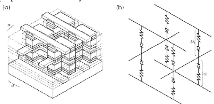
As previously underlined, RRAM memories are still in a R&D stage and only few memory circuits have been pub-lished in the literature. As memory elements may be inte-grated into BEOL, RRAM technology is of particular inter-est for high density storage with possibly multi-levels three-dimensional architectures (Fig. 6a) [33,34]. Nevertheless, it has to be stressed out that from a memory cell and array design point of view, unipolar operations are preferred over bipolar operations.
For this promising class of memories, two cell architec-tures are generally proposed depending on the nature of RRAM element: 1T/1R (i.e. one transistor associated with one resistive element) for CMOS-based active matrix; 1R enabling crossbar-type memory passive matrix. The first demonstrators integrated memory cells with size of 4-8 F2
for active matrix and (4/n) F2 for a passive matrix (i.e.
crossbar) with n storage layers [25,32]. Nevertheless, in passive crossbars, the memory elements cannot be electri-cally isolated while neighboring cells are addressed. This problem can be solved by adding serial elements with a specific (high) non-linearity (e.g. diode as shown in Fig. 6b)
at each resistively switching cell, depending on the resisting properties and the array size.
Figure 6. Three-dimensional view (a) and schematic (b) of a two-layer crossbar memory array integrating 1 diode/1 resistor (1D/1R) core-cells. 1D/1R cell enables isolating a memory element while neighbouring cells are addressed.
Samsung Company already demonstrated a “non-CMOS” solution with a two-layer architecture based on 1D/1R memory cells associating a diode with a nickel oxide-based resistive element exhibiting unipolar switching [35]. Such a crossbar memory matrix was easily designed with the help of BL and WL to access each cell individually.
CBRAM derives from parent technology PMC, which was developed by Axon TC in collaboration with Arizona State University. In 2007, Qimonda/Altis/Infineon consorti-um demonstrated a 2 Mb CBRAM test chip with read-write control circuitry implemented in a 90 nm technological node with read/write cycle time less than 50 ns [36]. The corre-sponding CBRAM circuit was developed using 8 F2
core-cells associating 1 MOS transistor with 1 Conductive Bridg-ing Junction (i.e. 1T/1CBJ). The chip design was based on a fast feedback regulated CBJ read voltage and on a novel program charge control using dummy cell bleeder devices. It has to be mentioned that Adesto startup has acquired intellectual property and patents related to CBRAM tech-nology from Qimonda in October 2010. In addition, Adesto announced in November 2010 a manufacturing partnership with Altis Semiconductor.
The low power resistive switching at voltages below 1 V, the ability to scale to minimum geometries below 20 nm and the multi-level capability make CBRAM a very promising non volatile emerging memory technology. Nevertheless, as compared to prototypical MRAM, FRAM and PCM memo-ries, CBRAM concept requires refresh operations due to the poor retention capability in low resistance state (contrary to the high resistive state which is usually much more stable in time). Thus, a refresh voltage is applied to the CBRAM memory element at a predetermined time to strengthen and stabilize low resistance state. This smart refresh enables preserving the resistance margin ΔR necessary to unambig-uously discriminate high and low resistance states during read. This refresh is performed without destroying data stored in CBRAM element whereas in DRAM a rewriting of respective state is mandatory.
To conclude, RRAM technology is very promising and once again many design solutions exist for implementation.
However, depending on RRAM concept, specific peripheral circuits are required to guaranty reliable memory operations.
VI. TWO GUIDING PRINCIPLES
For both prototypical (MRAM, PCM) and emerging (RRAM) technologies, two guiding principles are shared for designing generic resistive switching memory circuits:
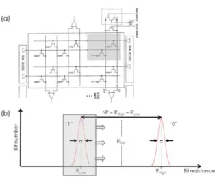
The first guideline is related to the implementation of bi-stable resistive elements in a memory array. In most of cases, memory cells rely on the association of a se-lect/access device with a resistive element. Depending on the resistive concept (magnetic, phase change or re-dox), the select/access device can be a BJT, a MOS tran-sistor or a diode. Even if MOS trantran-sistor is frequently preferred, access device is adapted to electrical charac-teristics of resistive element (set and reset currents and voltages, resistance levels, memory window…). To ac-cess each 1T/1R memory cell individually, suited bias conditions are applied to Bit (BL), Source (SL) and Word (WL) Lines of the addressed cell, other lines being grounded and/or floating. For illustration, Hush and Baker [37] have proposed an architecture for sensing the resistance state of a programmable conductor random access memory element (Fig. 7a). The design is based on complementary memory elements, one holding the re-sistance state being sensed and the other holding a com-plementary resistance state. A sense amplifier detects voltages discharging through high and low resistance el-ements to determine the resistance state.
Resistance in “0” and “1” states represents the second common guideline (Fig. 7b). Indeed, reliable read opera-tions require an unambiguous discrimination of low and high resistances, below and above the median resistance RRef defined as R/2 = [RHigh – RLow]/2. Moreover, the
bit cell resistance distributions must be narrow to avoid any overlap between “0” and “1” states (i.e. large R/ ratio, with the distribution standard deviation). Finally, as the maximum current consumed during read operation is linked to RLow, resistance in “1” state must be as large
as possible to decrease overall power consumption.
Figure 7. (a) Architecture that enables sensing the resistance state of a programmable conductor random access memory element using comple-mentary resistive elements (dashed square). (b) Bit cell resistance distribu-tions of “0” and “1” resistance states.
VII. CONCLUSION
In summary, reliable memory operations require a close matching between electrical characteristics of resistive ele-ments and design rules. In other words, to reach suitable sensing margin (i.e. large R) shifted toward high resistanc-es altogether with narrow bit cell rresistanc-esistance distributions (i.e. low ), it is of primary importance to:
Control materials microstructure, critical dimensions of memory element, process variability…;
Understand physical mechanisms explaining resistance switching;
Develop relevant compact models to be implemented in electrical simulators.
Hence, the development of prototypical and emerging memory concepts emphasizes the necessity to make stronger links between memory cell materials and processes, model-ing and circuit design.
REFERENCES
[1] J. Van Houdt, R. Degraeve, G. Groeseneken, and H.E Maes, “Physics of Flash memories”, in Nonvolatile memory technologies with
empha-sis on Flash, J.E. Brewer and M. Gill, Eds. Hoboken: John Wiley &
Sons Inc., 2008, pp. 129-177.
[2] J.F. Scott, Ferroelectric memories. Berlin, Springer, 2000.
[3] Ch. Muller, D. Deleruyelle, and O. Ginez, “Emerging memory con-cepts: materials, modeling and design”, in Handbook of Design
Tech-nology for Heterogeneous Embedded Systems, I. O’Connor, G.
Ni-colescu and C. Piguet, Eds. Springer, to be published in 2011 (ISBN: 978-94-007-1124-2).
[4] ITRS, International Technology Roadmap for Semiconductors, “Potential and Maturity of Selected Emerging Research Memory Technologies”, 2011 (http://www.itrs.net).
[5] B.C. Lee, E. Ipek, O. Mutlu, and D. Burger, “Architecting phase change memory as a scalable DRAM alternative”, ACM SIGARCH
Computer Architecture News, vol. 37, no. 3, pp. 2-13, 2009.
[6] Ch. Muller, D. Deleruyelle, R. Müller, M. Thomas, A. Demolliens, Ch. Turquat, and S. Spiga, “Resistance change in memory structures integrating CuTCNQ nanowires grown on dedicated HfO2 switching
layer”, Solid-State Electronics, vol. 56, no. 1, pp. 168-174, 2011. [7] A. Sawa, “Resistive Switching in Transition Metal Oxides”, Materials
Today, vol. 11, no 6, pp. 28-36, 2008.
[8] C. Dumas, D. Deleruyelle, A. Demolliens, Ch. Muller, S. Spiga, E. Cianci, M. Fanciulli, I. Tortorelli, and R. Bez, “Resistive switching characteristics of NiO films deposited on top of W and Cu pillar bot-tom electrodes”, Thin Solid Films, vol. 519, no. 11, pp. 3798-3803, 2011.
[9] M.N. Kozicki, M. Park, and M. Mitkova, “Nanoscale memory elements based on solid-sate electrolytes”, IEEE Trans. Nanotechnology, vol. 4, no. 3, pp. 331-338, 2005.
[10] S. Tehrani, “Status and outlook of MRAM memory technology”,
IEEE Proc. of Int. Electron Device Meeting, pp. 1-4, 2006.
[11] T.W. Andre, J.J. Nahas, C.K. Subramanian, B.J. Garni, H.S. Lin, A. Omair, and W.L. Martino, “A 4 Mb 0.18 µm 1T1MTJ Toggle MRAM with balanced three input sensing scheme and locally mirrored unidirectional write drivers”, IEEE J. Solid State Circuits, vol. 40, no. 1, pp. 301-309, 2005.
[12] I.L. Prejbeanu, W. Kula, K. Ounadjela, R.C. Sousa, O. Redon, B. Dieny, and J.P. Nozières, “Thermally assisted switching in
exchange-biased storage layer magnetic tunnel junctions”, IEEE Trans. Magn., vol. 40, no. 4, pp. 2625-2627, 2004.
[13] Nagai Hide, Huai Yiming, Ueno Shuichi, and Koga Tsuyoshi, “Spin-Transfer Torque writing technology (STT-RAM) for future MRAM”,
IEIC Technical Report, vol. 106, no. 2, pp. 73-78, 2006.
[14] Zhitao Diao, Zhanjie Li, Shengyuang Wang, Yunfei Ding, Alex Panchula, Eugene Chen, Lien-Chang Wang, and Yiming Huai, “Spin-transfer torque switching in magnetic tunnel junctions and spin-transfer torque random access memory”, J. Phys.: Condens. Matter, vol. 19, no. 16, pp. 165209-165221, 2007.
[15] M. Hosomi, H. Yamagishi, T. Yamamoto, K. Bessho, Y. Higo, K. Yamane, H. Yamada, M. Shoji, H. Hachino, C. Fukumoto, H. Nagao, and H. Kano, “A novel nonvolatile memory with spin torque transfer magnetization switching: spin-RAM”, IEEE Proc. of Int. Electron
Device Meeting, pp. 459-462, 2005.
[16] Y. Guillemenet, L. Torres, and G. Sassatelli, “Non-volatile run-time field-programmable gate arrays structures using thermally assisted switching magnetic random access memories”, IET Computers and
Digital Techniques, vol. 4, no. 3, pp. 211-226, 2010.
[17] W. Zhao, E. Belhaire, and C. Chappert, “Spin-MTJ based non volatile flip-flop”, IEEE Review of Advances on Micro, Nano, and Molecular
Systems, vol. 1, pp. 399-402, 2007.
[18] S.R. Ovshinsky, “Reversible electrical switching phenomenon in disordered structures”, Phys. Rev. Lett., vol. 21, no. 20, pp. 1450-1453, 1968.
[19] M.H.R. Lankhorst, B.W. Ketelaars, and R.A. Wolters, “Low-cost and nanoscale non-volatile memory concept for future silicon chips”, Nat.
Mater., vol. 4, no. 4, pp. 347-352, 2005.
[20] W.Y. Cho, B-H. Cho, B-G. Choi, H-R Oh, S. Kang, K-S. Kim, K-H. Kim, D-E. Kim, C-K. Kwak, H-G. Byun, Y. Hwang, S. Ahn, G-H. Koh, G. Jeong, H. Jeong, and K. Kim, “A 0.18 µm 3.0 V 64 Mb non-volatile Phase transition Random Access Memory (PRAM)”, IEEE J.
Solid-State Circuits, vol. 40, no. 1, pp. 293-300, 2005.
[21] M. Gill, T. Lowrey, and J. Park, “Ovonic unified memory – a high-performance nonvolatile memory technology for stand-alone memory and embedded applications”, IEEE Proc. of Int. Solid State Circuits
Conf., vol. 1, pp. 202-204, 2002.
[22] J.H. Oh, J.H. Park, Y.S. Lim, H.S. Lim, Y.T. Oh, J.S. Kim, J.M. Shin, Y.J. Song, K.C Ryoo, D.W. Lim, S.S. Park, J.I. Kim, J.H. Kim, J. Yu, F. Yeung, C.W. Jeong, J.H. Kong, D.H. Kang, G.H Koh, G.T. Jeong, H.S. Jeong, and K. Kim, “Full integration of highly manufacturable 512Mb PRAM based on 90nm technology”, IEEE Proc. of Int.
Electron Device Meeting, pp. 49-52, 2006.
[23] Hyung-rok On, Beak-hyung Cho, Woo Yeong Cho, Sangbeom Kang, Byung-gil Choi, Hye-jin Kim, Ki-sung Kim, Du-eung Kim, Choong-keun Kwak, Hyun-geun Byun, Gi-tae Jeong, Hong-silk Jeong, and Kinam Kim, “Enhanced write performance of a 64 Mb phase-change random access memory”, IEEE J. Solid State Circuits, vol. 41, no. 1, pp. 122-126, 2006.
[24] F. Bedeschi, C. Resta, O. Khouri, E. Buda, L. Costa, M. Ferraro, F. Pellizzer, F. Ottogalli, A. Pirovano, M. Tosi, R. Bez, R. Gastaldi, and G. Casagrande, “An 8 Mb demonstrator for high-density 1.8 V phase-change memories”, IEEE Proc. of VLSI Circuits Symp., pp. 442-445, 2004.
[25] R. Waser, and M. Aono, “Nanoionics-based resistive switching mem-ories”, Nature, vol. 6, pp. 833-840, 2007.
[26] R. Waser, R. Dittmann, G. Staikov, and K. Szot, “Redox-Based Resistive Switching Memories – Nanoionic Mechanisms, Prospects, and Challenges”, Adv. Mater., vol. 21, pp. 2632-2663, 2009. [27] D.B. Strukov, G.S. Snider, D.R. Stewart, and R.S. Williams, “The
missing memristor found”, Nature, vol. 453, pp. 80-83, 2008. [28] R. Meyer, L. Schloss, J. Brewer, R. Lambertson, W. Kinney, J.
Sanchez, and D. Rinerson, “Oxide dual-layer memory element for scalable non-volatile cross-point memory technology”, IEEE Proc. of
Non Volatile Memory Technology Symp., pp. 54-58, 2008.
[29] L. Courtade, Ch. Turquat, J.G. Lisoni, L. Goux, D.J., Wouters, D. Deleruyelle, and Ch. Muller, “Integration of resistive switching NiO in small via structures from localized oxidation of nickel metallic layer”, IEEE Proc. of European Solid State Device Research Conf., pp. 218-221, 2008.
[30] L. Courtade, J. Lisoni-Reyes, L. Goux, C. Turquat, Ch. Muller, and D.J. Wouters, “Method for manufacturing a memory element comprising a resistivity-switching NiO layer and devices obtained thereof”, US Patent no. 2009/0152526 A1, Published June 18 (2009). [31] L. Goux, J.G. Lisoni, M. Jurczak, D.J. Wouters, L. Courtade, Ch.
Muller, “Coexistence of the bipolar and unipolar resistive switching modes in NiO cells made by thermal oxidation of Ni layers”, J. Appl.
Phys., vol. 107, no. 2, pp. 024512(1–7), 2010.
[32] R. Symanczyk, R. Dittrich, J. Keller, M. Kund, G. Muller, B. Ruf, P.-H. Albarede, S. Bournat, L. Bouteille, and A. Duch, “Conductive bridging memory development from single cells to 2Mbit memory arrays”, IEEE Proc. of Non Volatile Memory Technology Symp., pp. 71-75, 2007.
[33] C. Kügeler, M. Meier, R. Rosezin, S. Gilles and R. Waser, “High density 3D memory architecture based on the resistive switching effect”, Solid-State Electronics, vol. 53, no. 12, pp. 1287-1292, 2009. [34] I.G. Baek, D.C. Kim, M.J. Lee, H-J. Kim, E.K. Yim, M.S. Lee, J.E.
Lee, S.E. Ahn, S. Seo, J.H. Lee, J.C. Park, Y.K. Cha, S.O. Park, H.S. Kim, I.K. Yoo, U-In Chung, J.T. Moon, and B.I. Ryu, “Multi-layer cross-point binary oxide resistive memory (OxRRAM) for post-NAND storage application”, IEEE Proc. of International Electron
Devices Meeting, pp. 750-753, 2005.
[35] Myoung-Jae Lee, Youngsoo Park, Bo-Soo Kang, Seung-Eon Ahn, Changbum Lee, Kihwan Kim, Wenxu Xianyu, G. Stefanovich, Jung-Hyun Lee, Seok-Jae Chung, Yeon-Hee Kim, Chang-Soo Lee, Jong-Bong Park, and In-Kyeong Yoo, “2-stack 1D-1R cross-point structure with oxide diodes as switch elements for high density resistance RAM applications”, IEEE Proc. of Int. Electron Device Meeting, pp. 771-774, 2007.
[36] S. Dietrich, M. Angerbauer, M. Ivanov, D. Gogl, H. Hoenigschmid, M. Kund, C. Liaw, M. Markert, R. Symanczyk, L. Altimime, S. Bournat, and G. Mueller, “A nonvolatile 2-Mbit CBRAM memory core featuring advanced read and program control”, IEEE J.
Solid-State Circuits, vol. 42, no. 4, pp. 839-845, 2007.
[37] G. Hush, and J. Baker, “Complementary bit PCRAM sense amplifier and method of operation”, US Patent no. 6,791,859 B2, Published September 14, 2004.