Publisher’s version / Version de l'éditeur:
Condensed Matter, 2017-06-22
READ THESE TERMS AND CONDITIONS CAREFULLY BEFORE USING THIS WEBSITE. https://nrc-publications.canada.ca/eng/copyright
Vous avez des questions? Nous pouvons vous aider. Pour communiquer directement avec un auteur, consultez la
première page de la revue dans laquelle son article a été publié afin de trouver ses coordonnées. Si vous n’arrivez pas à les repérer, communiquez avec nous à [email protected].
Questions? Contact the NRC Publications Archive team at
[email protected]. If you wish to email the authors directly, please see the first page of the publication for their contact information.
NRC Publications Archive
Archives des publications du CNRC
This publication could be one of several versions: author’s original, accepted manuscript or the publisher’s version. / La version de cette publication peut être l’une des suivantes : la version prépublication de l’auteur, la version acceptée du manuscrit ou la version de l’éditeur.
Access and use of this website and the material on it are subject to the Terms and Conditions set forth at
Atomic silicon quantum dot wires and logic gates for binary
computation
Huff, Taleana; Labidi, Hatem; Rashidi, Mohammad; Achal, Roshan;
Livadaru, Lucian; Dienel, Thomas; Pitters, Jason; Wolkow, Robert A.
https://publications-cnrc.canada.ca/fra/droits
L’accès à ce site Web et l’utilisation de son contenu sont assujettis aux conditions présentées dans le site LISEZ CES CONDITIONS ATTENTIVEMENT AVANT D’UTILISER CE SITE WEB.
NRC Publications Record / Notice d'Archives des publications de CNRC:
https://nrc-publications.canada.ca/eng/view/object/?id=4a09ac95-e09c-462a-b266-f5ce2115f337 https://publications-cnrc.canada.ca/fra/voir/objet/?id=4a09ac95-e09c-462a-b266-f5ce2115f337Taleana Huff1,3,∗, Hatem Labidi1,2, Mohammad Rashidi1, Roshan
Achal1,3
, Lucian L, Thomas D, Jason , and Robert A. Wolkow1,2,3,∗ 1
Department of Physics, University of Alberta, Edmonton, Alberta, T6G 2J1, Canada 2
National Institute for Nanotechnology, National Research Council of Canada, Edmonton, Alberta, T6G 2M9, Canada 3
Quantum Silicon, Inc., Edmonton, Alberta, T6G 2M9, Canada, ∗email: [email protected]; [email protected]
(Dated: October 26, 2017)
Nanoelectronics has long striven for the ultimate limit of fabrication: reliable use of single atoms as building blocks for computational components. This has required years of development in tools not only to manipulate single atoms with sub-angstrom precision, but also tools that can read the sensitive outputs and dynamics. Here, we report the first example of reversible information transmission through an atomic silicon quantum dot fabricated binary wire and OR gate. We used an atomic force microscope operating in the non-contact regime (NC-AFM) to fabricate, read the output, and actuate both the wire and gate into different readable states. These changes are clearly seen in both raw AFM images, and in kelvin probe force microscopy (KPFM) spectroscopy taken above the silicon quantum dots. This sets the platform for a potential new class of ultra-fast, ultra-power efficient, and ultra dense computing.
INTRODUCTION
The promise of atom scale computing first became a possi-bility when Eigler et al. controllably moved atoms on a sur-face to achieve structures of their design [1]. In a subsequent work, the same lab made molecular cascades where, in anal-ogy to falling dominoes, a terminal molecule was tipped to, in turn, tip over a neighboring molecule, which tipped the next molecule, and so on [2]. Separate branches of the cascade were delicately timed to come together in such a way as to achieve binary logic functions. With these results a new era was begun. However, challenges preventing practical applica-tions remained and those limitaapplica-tions have been very difficult to overcome. Some of those challenges are; 1) the need to have the patterned atoms be robust at practical operation tem-peratures ideally room temperature. The initial atomic pat-terns were very delicately bound and would not persist above about -280◦C [1, 2]. In general, atom fabrication of structures
robust enough to withstand relatively high operating tempera-ture are more difficult to make. This is because larger energy inputs from the scanned probe are required to dislodge and move strongly bound atoms, and under such conditions cova-lent bonds within the probe itself break with some probability comparable to that of the target bond [3]. 2) The patterned atoms need to be electrically distinct from the substrate so as to enable conduction pathways that are not shorted-out or al-tered by the substrate. Studies performed on metals [4, 5], the most common choice, were therefore limited in that regard. Isolation has been achieved in studies of metal atoms and of molecules separated from a metal substrate by a salt layer, but these have their limitations in uniformity of layer thickness and issues with spontaneous loss of charge to the substrate [6, 7]. 3) The atomic circuitry must not require mechanical or other reset processes (analogous to standing all the domi-noes back up) that would prevent the circuitry being instantly reusable.
The above are necessary, but far from sufficient qualities of
a working atomic scale circuitry. Ideally, and to justify the substantial retooling required, a new circuitry should be more than compact. In order to provide a path beyond the estab-lished semiconductor roadmap, it must address the particular limitations of todays dominant, and very nearly mature CMOS technology; the primary problem being excessive power den-sity which causes devices to become hot.
By putting aside transistor-based logic that sinks a burst of electrons to ground with every cycle of the clock, to consider-ing field controlled computconsider-ing schemes such as quantum dot cellular automata [8], it is possible, in principle, to expend only the entropic energy associated with rearranging, but not disposing of electrons. As the load of such circuits present to the clock is essentially reactive, there is the opportunity for very low power and fast resonant clocking also.
These types of low power field controlled binary logic ele-ments formed of quantum dot ensembles have been hypothe-sized, and even rudimentarily realized, for over a decade now [8–11]. Single electrons, or their absence, serve as 1 and 0 inputs and, likewise, the logic state at the output is repre-sented by a localized charge, the value of which can be read and transmitted by a two-state wire to serve as inputs to sub-sequent logic elements. Clocking circuitry provides gain by restoring such transmitted signals [8]. It is necessary that electrons exhibit ground state behavior for such quantum dot circuities to operate. If, as typical, the quantum dots are of a size that requires cryogenic conditions to ensure dominant ground state electronic behavior, circuitry built of such dots would also need to operate at cryogenic conditions; a limiting to condition for many applications.
In this work we describe a path forward that addresses these various concerns and is based upon the atomic silicon quan-tum dot (ASiQD) [12]. ASiQDs, or desorbed single hydrogen atoms from the passivated H-Si(100) surface display quantum dot like behavior in that they can be occupied by 2, 1, or 0 electrons depending on surface doping, surface to bulk poten-tial, and their proximity to each other [13]. These are often
2 colloquially referred to as dangling bonds (DBs) in the
liter-ature, but here we use the term ASiQD to imply a vessel for holding electrons and for forming QD ensembles of higher function, whereas the less specific term dangling bond is used when discussing surface states and their interaction with the bulk at larger applied voltages than involved here.
Using ASiQD, binary atomic silicon logic (BASIL) circuit elements with a bit energy of the order of several 100 meV are demonstrated. This bit energy, somewhat larger than kT, is desirable as information is held just stably enough to with-stand environmental noise, while the barrier to purposeful ma-nipulation of data is not so large, as in CMOS today, that excessive energy must be expended to achieve computation inadvertently causing device heating. Prior work also sug-gests these BASIL circuit elements will work at room tem-perature, addressing the need for a paradigm not limited by cryo-temperatures [14].
In addition to being small and, therefore, having very large intra-dot energy level spacing, the ASiQDs can be placed very close allowing relatively large interaction energies of or-der 100 meV [12]. Correspondingly, the tunnel rate between coupled ASiQDs is of order 10 THz for closest spaced dots [14, 15], a large increase over more conventional coupled dots where a rate of GHz is more typical [16]. Tunnel period is a key indicator of information transmission speed along lines of field-coupled bi-stable tunneling oscillators as will be de-scribed in the following.
Furthermore, previous work has shown that these ASiQDs can be lithographically patterned with atomic precision using applied voltage pulses with scanning probe microscope tips [17, 18]. Recent work has also shown a powerful capability in lithographic error correction with misplaced ASiQDs erased using ”capping” as described in [19], a functionality used to actuate the OR gate as demonstrated later. As the dots contain only one atom, dot size dispersion is zero leading to homo-geneity of circuit properties when patterned. And, because the dots are placed on silicon crystalline lattice positions, in-homogeneity related to inter dot spacing is also eliminated.
One further essential characteristic of the atomic circuitry described here must be borne in mind. This relates to the ear-lier stated need to achieve circuit and substrate isolation. An essential quality of the silicon atom states is that they exist in the silicon substrate band gap. This naturally achieves the substrate-to-atom circuitry electrical isolation required, with-out the need of a distinct insulating layer. This will prove to be a principal property as it allows isolation, or selective spa-tial and temporal connection to the bulk at will. As has been shown recently, under these conditions bulk-to-surface state conduction is absent unless a substantial surface to bulk po-tential is applied [12].
With that in mind, NC-AFM is an optimal tool to look at the charge state switching of these BASIL assemblies. NC-AFM has been proven as a tool capable of resolving differ-ently charged adatoms and molecular species, as well as serv-ing to switch the charge state of said molecules and atoms [7, 20]. Kelvin probe force microscopy specifically has been
widely applied to study the contact potential difference be-tween probe and sample with different charges on molecules and atoms altering the signature. [7, 21] In our approach, we use these powerful capabilities to examine atomic charge transfer between the potential wells of tunnel coupled BASIL patterns in a notably minimally-perturbative way, unlike the previous STM analysis of such phenomena. Additionally, we show reversibility by using the ”capping”, or erasure of ASiQDs to reset outputs of the gate.
RESULTS AND DISCUSSIONS
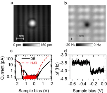
Earlier experimental and theoretical work established that on highly doped n-type silicon crystals, isolated ASiQDs on the H-Si(100) surface spontaneously accept an additional electron to become occupied by 2 electrons and negatively charged [13, 14, 22–24]. Hence, under the conditions of this study, we expect the ASiQD to be negatively charged at zero bias. However, when sweeping bias, the ASiQD should be-come neutral upon application of a modest negative sample bias (in the order of ≈ -200 mV), and, at higher voltages (usu-ally -1 V or higher) the ASiQD again becomes negative as the depletion barrier separating bulk and surface is overcome allowing the conduction band electrons to fill the ASiQD [17]. The transition of the ASiQD from a negatively charge state at zero bias, to the neutral state at small negative sample bias has been inferred, but never seen because no current is avail-able in the bandgap to generate an STM image or current-voltage spectrum in that low current-voltage range. In Figure 1 we show the first experimental evidence of this priorly unseen transition using AFM.
Figure 1-a shows a constant current STM image of an ASiQD created by tip-induced desorption of a single hydro-gen atom from the H-Si(100) surface. At relatively high volt-ages (e.g. -1.7 V), the negatively charged ASiQD appears in filled states images as a bright protrusion surrounded by a characteristic small dark halo [17]. In the corresponding fre-quency shift map at 0 V (Figure 1-)). hydrogen atoms decorat-ing underneath silicon atoms appear as bright protrusions ar-ranged in the 2×1 surface reconstruction. The ASiQD shows up as a dark feature indicating a much higher tip-sample at-tractive interaction [19].
Figure 1-c shows I(V) spectroscopy curves taken above the ASiQD and H-Si surface, with both the surface and ASiQD showing a zero current bandgap from around -0.8 to +0.2 V. Figure 1-d shows the∆f (V) spectra, i.e. KPFM spectroscopy, measured above the ASiQD with a bias sweep range of -0.6 to 0 V, a range in the bandgap of the material where no STM information would be available. Interestingly, a sharp step is seen at around -250 mV. Prior work examining charged species [6, 21], electron transfer between molecules [7], and charge state changes in quantum dots [25] in NC-AFM ex-periments has shown this type of step feature to correspond to a dynamic single-electron charge state change. Therefore, based on previous works, the step seen in Figure 1-d can be
a b c d 1 nm 1 nm 0 pm 150 pm -20 Hz 0 Hz -2 -1 0 1 2 0.11 10 100 -0.6 -0.4 -0.2 0.0 -4.5 -4.0 -3.5 -3.0 Current (pA) Sample bias (V) DB H-Si f (Hz) Sample bias (V)
FIG. 1. Probing charge State Transition in an Atomic Silicon Quantum Dot using NC-AFM(a) 3x3 nm filled states STM image (-1.7 V and 50 pA) and (b) corresponding frequency shift map at 0 V of an ASiQD (zrel=-350 p.m and Amp=100 p.m). (c) Current
vs. Bias spectroscopy plotted in log scale of the ASiQD (black) and hydrogen terminated surface (red). (d) Frequency shift as a function of voltage measured above the ASiQD.
assigned to the charge state transition of the ASiQD from neg-ative (doubly occupied) to neutral (singly occupied) charge state, respectively right and left of the step in the∆f (V) curve around -250 mV.
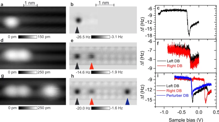
We will now examine structures constructed from multi-ple ASiQD. When 2 ASiQDs are closely spaced, within about 1 nm or less, Coulombic repulsion causes one of the pair’s extra electrons to delocalize in the conduction band [14, 22]. That loss of an electron creates an unoccupied state in the pair of ASiQDs. That, and the low ( 0.5 eV) and narrow barrier be-tween the atoms makes tunneling bebe-tween the paired ASiQDs possible. Figure 2 explores polarization of one of these tunnel coupled pairs of ASiQDs.
Figure 2 (a) and (b) show an STM image of an isolated ASiQD and the corresponding frequency shift map. The∆f (V) spectra (Figure 2 (c)) shows a charge transition step at -0.2 V, We now add on to the ensemble, but with care taken to ensure no tip changes with the addition of ASiQDs, and with identical parameters for AFM and KPFM. In Figure 2 (d) a second ASiQD is created that is tunnel coupled to the first ASiQD from (b). The AFM image in (e) shows 1 intervening hydrogen atom between the pair, with a similar contrast ob-served above both ASiQDs. The KPFM measurement in (h) corroborates this, showing nearly identical AFM curves taken over the 2 ASiQDs, with the charge transition step shifted to a less negative value occurring now around -0.25 V. We recall that the tunnel coupled pair of ASiQDs, collectively, have a charge of -1, which may account for this horizontal shift.
Finally, a 3rd ASiQD is added in (g), with the AFM image
in (f) showing a 4 H atom separation. This perturbing ASiQD is not significantly tunnel coupled to the pair as the tunneling interaction falls off exponentially, nor Coulombically desta-bilized enough to lose its negative charge. A stark contrast is now noticed in tunnel coupled pair. The middle ASiQD is significantly lighter than the farthest ASiQD. Delving deeper and looking at the KPFM curves for this ”2+1” experiment in Figure 2 (i) (a color coded inset is in the bottom left of (i)), we notice that the KPFM transition energies for the perturb-ing ASiQD (black) and for the ASiQD furthest left(blue) are markedly more negative than the middle ASiQD (red). The KPFM trace for the middle ASiQD shows a distinctly shifted charge transition energy to +200 mV. This shift is due to the repulsive effect of the perturbing ASiQD. We see that a less negative voltage between probe and sample must be applied to record the negative to neutral charge state transition of this ASiQD. Expressed otherwise, we see that the middle ASiQD at zero probe bias, but under the influence of the negative per-turbing ASiQD, is already in the neutral state. It is evident that the tunnel coupled ASiQDs form a double well potential that can be polarized by an electric perturbation. In this example, the double well is tilted to the left causing the shared electron to tend to localize there.
This is our central result for the construction of multiple ASiQD structure such as binary wires. A fixed charge, or a variable bias electrode, can localize charge to one side of a double well potential formed of two tunnel coupled ASiQDs. This allows information to be encoded in spatial charge distri-butions and, as we will see shortly, for information to be trans-ferred without the use of a conventional current, with mini-mal energy consumption per operation, and with no quiescent power consumption. We can now expand on this principal.
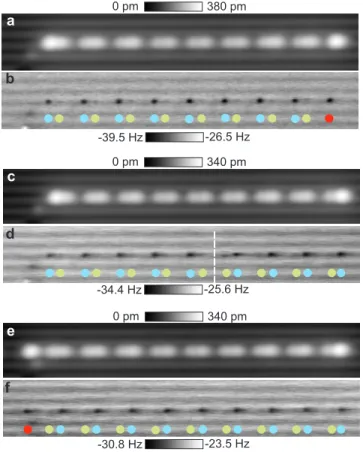
Figure 3 and 4 show multiple DB pairs aligned end to end, creating atomic binary wires and atomic binary gates. STM images shown in these figures reveal the position of atoms. On the other hand, AFM images in certain height regimes show the position of charges in the structure, and therefore reveal the logical state of the atomic wires or gates. Note that the AFM images were taken at larger tip-sample separations where electrostatic forces are dominant in order to visualize the transmission of information easier. Therefore, they do not resolve the surface structures as seen in Reference [26] and Figure 1 and 2.
Figure 3 shows a STM filled states image of a fabricated 17, 18 and 19 ASiQD atomic binary wires. Colored circles underneath each structure is added for clarity to show the po-sition of negative (blue), neutral (light green) and perturber (red) ASiQDs. Figure 3 shows an atomic binary wire consist-ing of 8 coupled pairs and a lone un-coupled DB actconsist-ing as a perturber on the far right. DBs in a pair have a single H atom separation, and pairs are 4 H atoms from each other. Below the STM image in 3 (a) is a constant height AFM image of the ensemble in (b). As before, the far right single perturbing charge breaks the symmetry and induces all pairs to align in one of the two available polarized states (tipping left). Fig-ure 3 (c) shows a STM image of the re-symmetrization of the
4
1 nm
1 nm
a
b
c
f
i
eh
d
g
0 pm -26.5 Hz -14.6 Hz -20.0 Hz 0 pm 0 pm 150 pm -3.1 Hz -1.9 Hz -1.6 Hz 250 pm 250 pm-18
-15
-12
-9
-6
-9
-8
-7
-6
-1.0
-0.5
0.0
0.5
-15
-12
-9
f (Hz)
f (Hz)
Left DBRight DBf (Hz)
Sample bias (V)
Left DB Right DB Perturber DBFIG. 2. Polarization effect on a multiple Atomic Silicon Quantum dots structure. STM images (-1.8 V and 50 pA), frequency shift maps (zrel=-380 p.m and Amp=100 p.m) and frequency shift versus bias spectra (∆f (V)) for a single ASiQD (a)-(b)-(c), 2 tunnel coupled ASiQDs
(d)-(e)-(f) and a 2+1 structure (g)-(h)-(i) . The∆f (V) spectra are color-coded according to the arrows in AFM images
wire, with the far right DB now turned into a coupled pair. The wire reacts by dividing down the middle in the frequency shift map of figure 3 (d) with half falling left, and half falling right. The symmetry plain is marked with a dashed white ver-tical line in the AFM image. Finally, in figure 3 (e) and (f), the same line of pairs is polarized from the opposite side with a 19th DB added on the left. The wire responds by assuming the other remaining polarization state (tipping right), revers-ing what was shown in figure 3 (a).
Thus, we have demonstrated reversible information trans-fer expending only the entropic energy associated with rear-ranging electrons in coupled wells, while also showing, unlike falling dominoes, no reset of the line is needed. The two state line is instantly ready to function again. The scanned probe instrument is not a component of the device, it is only an ob-server. We do state here that we do not have ready access to a positive charge, but electrons could similarly be pulled instead of pushed if we did.
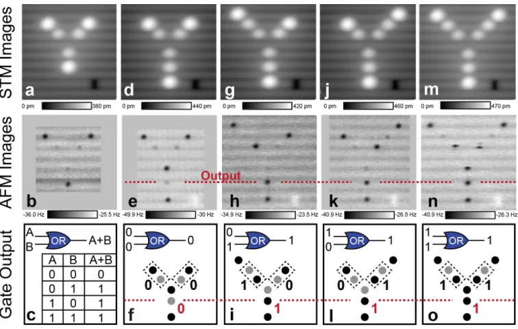
We show one final adaption of the basic principal estab-lished in Figure 2. Figure 4 shows a prototype binary logical OR gate. The two topmost branches are inputs, and the lower branch an output. Figure ?? (a) shows the ”central” struc-ture comprising the gate: 3 tunnel coupled pairs arranged at sharp angles and meeting in the center. Isolated from any elec-trostatic influence, the 2D assembly experiences elecelec-trostatic repulsion among the pairs, with electrons localizing to the out-side of the branches as indicated by the contrast in the AFM
frequency shift map in figure 4 (b).
We note again here the limitation that we can only ”push” with the negative charge of a perturbing ASiQD, not ”pull”. In order to establish an opposite polarization state of the output ASiQD, we make an adaption and fabricate a weak perturber at the terminus of the lower output branch as demonstrated in (d). This perturber acts as a ”weak spring”, polarizing the bot-tomost ASiQD from the central structure to be neutral, which we define as the 0 state. This is shown experimentally in (e) and graphically in (f). The first row of the truth table is estab-lished with two 0 inputs giving a 0 output.
When a negative input is in place at either the top left (g), top right (j), or both (m) input branches, the weak spring is overcome at the output with electrons in the structure re-arranging accordingly and flipping the 0 state of the output to a 1 state as seen in the AFM maps (h), (k), and (n) respectively. Correlating this to the gate output models (i),(l), and (o), this fulfills the rest of the truth table. To complete the truth table, figure 4 (j) was achieved by passivating the ASiQD input on the left in (g) using mechanical passivation, and creating the new input on the right.
CONCLUSION
In this paper we have demonstrated the essential capabil-ities required to build all-silicon, atom scale electronics for
0 pm 0 pm 0 pm -39.5 Hz -34.4 Hz -30.8 Hz 380 pm 340 pm 340 pm -26.5 Hz -25.6 Hz -23.5 Hz a b c d e f
FIG. 3. Information transmission through atomic silicon quan-tum dot (ASiQD) constructed binary wire(a) Filled states STM image and (b) corresponding frequency shift maps of a 17 ASiQD wire. Color guides are placed in (b) to show the location of the dots. (c) Symmetric 18 atom ASiQD wire creating from adding on the right of (a). (d) Frequency shift map of the dots showing the sym-metry splitting plane marked by the dashed white line (e) 19 atom wire with symmetry broken by adding a ASiQD on the left. (f) Fre-quency shift map showing the wire polarized to the right. All STM images were taken at V -1.7 and 50pA. All AFM images were taken at 0 V, with a relative tip elevation of z=330 p.m and an oscillation amplitude of 0.5 ˚A
binary computation. This approach might be dubbed SABL, for silicon atomic binary logic. Though not discussed here, it is evident that analog, and quantum electronics, can be built similarly.
Our primary building block is the atomic silicon quantum dot, first described in 2009 (prl). Crucially, this entity, and the ensembles of multiple dots as described here, exist in the sili-con band gap, enabling isolation of this 2 dimensional surface circuitry from the bulk without the need for an additional com-plicating insulating layer. As shown in recent work ( hatem NJP paper and 2 Moe papers,) highly local, indeed atom-scale connection of surface and bulk can be turned on as desired.
Spectra of local force as a function of applied voltage re-veal charge state transitions of single dangling bonds and of ensembles. Single electron induced switching of a double dot entity, and of a long sequence of double dots, from Left to Right or binary 0 and 1 states has been shown. A binary OR
gate including all states of its truth table have been shown. It is the focus of on-going work to show extension of signals well beyond the gate output as well as NOT and AND functions among others.
Because the gates and the binary wires between gates re-quire only single electron-level electrostatic actuation and be-cause no conventional current is required, power consump-tion will be extremely low. As the tunnel rate among coupled atomic quantum dots is of the order of femtoseconds ( NJP pa-per on qubits 2010) signal transmission and gating action will be fast. THz operation rates are anticipated. The approach described here may enable a beyond Moore technology com-bining as it does enormous speed with ultra low power con-sumption while eliminating transistors.
While we worked on a highly doped n-type substrate here, low doped and p-type doping will enable different charge states and modes of operation. Conventional local doping con-trol will allow mixed modes of operation and more complex function.
These studies were performed at liquid helium temperature because of enhanced instrument stability in that regime. How-ever, previous work shows polarization states as employed here persist at room temperature. Furthermore, the hydrogen terminated silicon system is known to be stable and free of any dangling bond/H atom diffusion to beyond 500K. Parallel work, not shown here, will provide environmental protection through encapsulation and connection of the atomic circuitry to ordinary lithographic features and to CMOS circuitry and is intended to enable operation in a normal packaged chip for-mat. Hybrid SABL CMOS circuitry of lower power con-sumption and or greater speed is targeted in the near term.
METHODS
Experiments were carried out using a commercial (Omi-cron) qPlus AFM system operating at 4.5 K. We used highly arsenic-doped (∼ 1.5×10¹⁹
atom cm−3) silicon (100).
Sam-ple preparation involved degassing at ∼ 600◦Cfor about 12
hours in ultra-high-vacuum (UHV), followed by a series of resistive flash anneals reaching 1250◦C. Secondary ion mass
spectroscopy done in prior works has shown similar heat treat-ments create a surface regime 60 nm deep where the dopant concentration is reduced near the surface, where the concen-tration is approximately 40 times less than that of the bulk [17, 27]. Then, while holding the Si substrate at 330◦C for
2 minutes, molecular hydrogen at106
Torr was cracked on a 1600◦C tungsten filament held approximately 10 cm from
the sample to create the 2×1 reconstructed hydrogen atom-terminated Si(100) surface.
We used qPlus AFM sensors [28] with a separate electrode for tunnel current. Focused ion beam (FIB) was used to cut a micro-tip from an electrochemically etched 50 µm polycrys-talline tungsten wire, then weld it to the sensor. This fab-rication technique ensured high sensitivity and well defined sensor mechanical properties [29].
6
FIG. 4. Prototype of a functional OR gate constructed using atomic silicon quantum dots (ASiQD). The first row shows constant current filled states STM images (-1.8V, 50pA) of the OR gate, and the second row the corresponding frequency shift maps (0V, Z 3.5 ˚A). The 3rd row includes the truth table of an OR gate (c), along with models for the switching inputs and outputs corresponding to the gate states displayed in rows one and two.
After being loaded in UHV, tips first had the oxide layer re-moved by several electron beam heating treatments followed by field evaporation cleaning of the apex in a field ion mi-croscope (FIM). Further sharpening was conducted using a FIM nitrogen etching process to obtain the smallest possible tip radius of curvature [29, 30]. Final in-situ tip processing was done through creation of a bare silicon patch through tip induced hydrogen desorption, followed by gentle controlled contacts with the tip on the reactive patch. This procedure usually results in a stable and artifact free tip [26].
To create an ASiQD, the tip is positioned on top of a sur-face hydrogen atom at 1.3 V and 50 pA, and applying pulses of 2.5 V for 10 ms. Mechanically induced covalent bonding of a single H atom at the tip apex and the silicon ASiQD to passivate it was done by following the procedure described in details in [19].
Nanonis control electronics and software were used for both STM and AFM data acquisition. For all frequency shift maps, Z=0 ˚A corresponds to the relative tip elevation defined by the STM imaging set points 50 pA and -1.8 V. To minimize drift during AFM image acquisition, the tip was left to settle for about 12 hours after approach to allow piezo scanner sta-bilization. Additionally, an atom tracking program was used.
All STM images are raw data.
ACKNOWLEDGMENT
We thank Martin Cloutier, Doug Vick, and Mark Salomons for their technical expertise. We thank NRC, NSERC, QSi, and AITF for financial support. We thank F. Giessibl for pro-viding us with the tuning forks for building the qPlus sensors.
[1] D. M. Eigler and E. K. Schweizer, Nature 344, 524 (1990). [2] A. J. Heinrich, C. P. Lutz, J. A. Gupta,
and D. M. Eigler, Science 298, 1381 (2002), http://science.sciencemag.org/content/298/5597/1381.full.pdf. [3] T. C. Shen, C. Wang, G. C. Abeln, J. R. Tucker, J. W.
Lyd-ing, P. Avouris, and R. E. Walkup, Science 268, 1590 (1995), http://science.sciencemag.org/content/268/5217/1590.full.pdf. [4] C. Joachim, J. K. Gimzewski, R. R. Schlittler, and C. Chavy,
Physical Review Letters 74, 2102 (1995).
[5] A. Yazdani, D. M. Eigler, and N. D. Lang, Science 272, 1921 (1996), http://science.sciencemag.org/content/272/5270/1921.full.pdf.
[6] W. Steurer, J. Repp, L. Gross, I. Scivetti, M. Persson, and G. Meyer, Physical Review Letters 114, 036801 (2015). [7] W. Steurer, S. Fatayer, L. Gross, and G. Meyer, Nature
com-munications 6 (2015), http://dx.doi.org/10.1038/ncomms9353. [8] C. S. Lent and P. D. Tougaw, Proceedings of the IEEE 85, 541
(1997).
[9] I. Amlani, A. O. Orlov, G. Toth, G. H. Bernstein, C. S. Lent, and G. L. Snider, Science 284, 289 (1999), http://science.sciencemag.org/content/284/5412/289.full.pdf. [10] K. Navi, R. Farazkish, S. Sayedsalehi, and M. R. Azghadi,
Microelectronics Journal 41, 820 (2010).
[11] A. O. Orlov, I. Amlani, G. H. Bernstein, C. S. Lent, and G. L. Snider, Science 277, 928 (1997), http://science.sciencemag.org/content/277/5328/928.full.pdf. [12] R. A. Wolkow, L. Livadaru, J. Pitters, M. Taucer, P. Piva,
M. Salomons, M. Cloutier, and B. V. C. Martins, “Sili-con atomic quantum dots enable beyond-cmos electronics,” in
Field-Coupled Nanocomputing: Paradigms, Progress, and Per-spectives, edited by N. G. Anderson and S. Bhanja (Springer Berlin Heidelberg, Berlin, Heidelberg, 2014) pp. 33–58. [13] L. Livadaru, J. Pitters, M. Taucer, and R. A. Wolkow, Phys.
Rev. B 84, 205416 (2011).
[14] M. B. Haider, J. L. Pitters, G. A. DiLabio, L. Livadaru, J. Y. Mu-tus, and R. A. Wolkow, Phys. Rev. Lett. 102, 046805 (2009). [15] L. Livadaru, P. Xue, Z. Shaterzadeh-Yazdi, G. A. DiLabio,
J. Mutus, J. L. Pitters, B. C. Sanders, and R. A. Wolkow, New Journal of Physics 12, 083018 (2010).
[16] S. D. Barrett and G. J. Milburn, Phys. Rev. B 68, 155307 (2003). [17] H. Labidi, M. Taucer, M. Rashidi, M. Koleini, L. Livadaru, J. Pitters, M. Cloutier, M. Salomons, and R. A. Wolkow, New Journal of Physics 17, 073023 (2015).
[18] L. Soukiassian, A. J. Mayne, M. Carbone, and G. Dujardin, Physical Review B 68 (2003), 10.1103/PhysRevB.68.035303. [19] T. Huff, H. Labidi, M. Rashidi, M. Koleini, R. Achal,
M. Salomons, and R. A. Wolkow, ArXiv e-prints (2017), arXiv:1706.05287 [cond-mat.mes-hall].
[20] L. Gross, F. Mohn, P. Liljeroth, J. Repp, F. J. Giessibl, and G. Meyer, Science 324, 1428 (2009).
[21] E. Bussmann and C. C. Williams, Applied Physics Letters 88, 263108 (2006).
[22] J. L. Pitters, L. Livadaru, M. B. Haider, and R. A. Wolkow, The Journal of chemical physics 134, 064712 (2011).
[23] S. R. Schofield, P. Studer, C. F. Hirjibehedin, N. J. Curson, G. Aeppli, and D. R. Bowler, Nature Communications 4, 1649 (2013).
[24] M. Taucer, L. Livadaru, P. G. Piva, R. Achal, H. Labidi, J. L. Pitters, and R. A. Wolkow, Physical Review Letters 112 (2014), 10.1103/PhysRevLett.112.256801.
[25] R. Stomp, Y. Miyahara, S. Schaer, Q. Sun, H. Guo, P. Grutter, S. Studenikin, P. Poole, and A. Sachrajda, Phys. Rev. Lett. 94, 056802 (2005).
[26] H. Labidi, M. Koleini, T. Huff, M. Salomons, M. Cloutier, J. Pitters, and R. A. Wolkow, Nature Communications 8, 14222 (2017).
[27] J. L. Pitters, P. G. Piva, and R. A. Wolkow, Journal of Vacuum Science & Technology B, Nanotechnology and Microelectron-ics: Materials, Processing, Measurement, and Phenomena 30, 021806 (2012).
[28] F. J. Giessibl, Applied Physics Letters 78, 123 (2001). [29] H. Labidi, M. Kupsta, T. Huff, M. Salomons, D. Vick,
M. Taucer, J. Pitters, and R. A. Wolkow, Ultramicroscopy 158, 33 (2015).
[30] M. Rezeq, J. Pitters, and R. Wolkow, The Journal of Chemical Physics 124, 204716 (2006).