HAL Id: hal-00566665
https://hal-iogs.archives-ouvertes.fr/hal-00566665
Submitted on 5 Apr 2012
HAL is a multi-disciplinary open access
archive for the deposit and dissemination of
sci-entific research documents, whether they are
pub-lished or not. The documents may come from
teaching and research institutions in France or
abroad, or from public or private research centers.
L’archive ouverte pluridisciplinaire HAL, est
destinée au dépôt et à la diffusion de documents
scientifiques de niveau recherche, publiés ou non,
émanant des établissements d’enseignement et de
recherche français ou étrangers, des laboratoires
publics ou privés.
Efficient photonic mirrors for semiconductor nanowires
Inbal Friedler, Philippe Lalanne, Jean-Paul Hugonin, Julien Claudon,
Jean-Michel Gérard, Alexios Beveratos, Isabelle Robert-Philip
To cite this version:
Inbal Friedler, Philippe Lalanne, Jean-Paul Hugonin, Julien Claudon, Jean-Michel Gérard, et al..
Efficient photonic mirrors for semiconductor nanowires. Optics Letters, Optical Society of America
-OSA Publishing, 2008, 33 (22), pp.2635-2637. �hal-00566665�
Efficient photonic mirrors for
semiconductor nanowires
I. Friedler,1P. Lalanne,1,*J. P. Hugonin,1J. Claudon,2J. M. Gérard,2A. Beveratos,3and I. Robert-Philip3
1
Laboratoire Charles Fabry de l’Institut d’Optique, CNRS, Universite Paris-Sud, Campus Polytechnique, RD 128, 91127 Palaiseau, France
2
Commissariat a l’Energie Atomique (CEA)/INAC/SP2M, Nanophysics and Semiconductor Laboratory, 17 Rue des Martyrs, 38054 Grenoble Cedex 9, France
3
Laboratoire de Photonique et de Nanostructures, CNRS, Route de Nozay, 91460 Marcoussis Cedex, France
*Corresponding author: [email protected]
Received August 25, 2008; revised September 29, 2008; accepted October 1, 2008; posted October 15, 2008 (Doc. ID 100618); published November 12, 2008
Using a fully vectorial frequency-domain aperiodic Fourier modal method, we study nanowire metallic mir-rors and their photonic performance. We show that the performance of standard quarter-wave Bragg mirmir-rors at subwavelength diameters is surprisingly poor, while engineered metallic mirrors that incorporate a thin dielectric adlayer may offer reflectance larger than 90% even for diameters as small as/5. © 2008 Optical Society of America
OCIS codes: 130.2790, 350.4238, 260.3910, 250.5590.
There is much current interest in the optical proper-ties of single-crystal nanowires, since their strong 2D confinement of electrons, holes, and photons make them particularly attractive as potential building blocks for nanoscale electronics and optoelectronic devices, including lasers [1–3], light detection in pho-tovoltaic devices [4], ultrasmall optical waveguides [5], and single-photon sources [6,7]. As shown by op-tical and electrical measurements, semiconductor nanowires can function as Fabry–Perot optical cavi-ties with mode spacing inversely related to the nano-wire length. Thus, the modal reflectance at the nano-wire termination (the facets for cleaved nanowires for in-stance) drastically impacts the photonic performance, such as the threshold current for lasers or the Q fac-tor for nanocavities [3], or even more basically, it may preempt radiation into an undesired facet and rein-force the directivity of the emitted light. Thus the re-alization of nanowire mirrors with high reflectance becomes crucial for applications.
In this Letter, we theoretically study the reflectiv-ity of GaAs nanowire facets for different kinds of mir-rors. We first show that standard Bragg mirrors are rather inefficient for wire diameters D⬍/3. By con-trast, we show that a high reflectance can be achieved for properly designed metallic mirrors. We consider both nanowires standing on a planar reflec-tor and nanowires terminated by a metallic post. For the first geometry, the reflectance exhibits a pro-nounced dip within the diameter range for single-mode operation, due to the excitation of surface plas-mon polaritons (SPPs). This effect can be quenched by incorporating a thin dielectric spacer layer be-tween the GaAs wire and metallic mirror, and a high reflectance 共R⬎90%兲 can be achieved for all single-mode wires. The second geometry, which is attractive due to the compactness of integrated post–mirrors, is not as efficient for small diameters, but offers a rather large reflectance共R⬎80%兲 for D⬎0.23.
In the following, we consider cylindrical nanowires made of high refractive index semiconductors such as
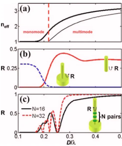
GaAs共n=3.45兲. The wires offer a strong 2D confine-ment of light in the transverse directions and guide light in the longitudinal z direction. Figure 1(a)
shows the normalized propagation constant neff
= kz/ k0for the fundamental HE11mode [8] as a func-tion of D /. The computational results are obtained at ␥= 950 nm, a wavelength corresponding to the emission line of single InAs quantum dots [7], with a fully vectorial frequency-domain aperiodic Fourier modal method (a-FMM) [9]. The overall dispersion of the guided mode can be separated into three repre-sentative regimes. For small diameters 共D⬍0.18兲,
neffis close to unity and the mode band is very close to the light line of the background free space. In this
Fig. 1. (Color online) (a) Effective index neff of the HE11 mode of a GaAs cylindrical nanowire as a function of the normalized diameter D /. The second mode is shown with a thin curve. (b) HE11modal reflectance of a cleaved facet in air (solid curve) and of a facet connecting with a GaAs substrate (dashed curve). (c) HE11modal reflectance of an
N-pair GaAs/ AlAs 共n=3.45/2.95兲 Bragg mirror composed
of /共4neff兲 thick layers for N=16 (solid curve) and N=32 (dashed curve). All results hold for=950 nm.
November 15, 2008 / Vol. 33, No. 22 / OPTICS LETTERS 2635
domain, the field is only weakly confined and a large fraction of the mode power witnesses the air back-ground. For D⬎0.3, neff is rather large, implying that the HE11field is almost entirely confined within the nanowire. Between the weak- and strong-confinement regimes lays an intermediate domain where the dispersion significantly deviates from the light lines of the air and GaAs materials. This repre-sents the interesting regime for most photonic appli-cations; monomode operation is guaranteed but more importantly, a large fraction of the spontaneous emis-sion of a dipole (a quantum dot for instance) embed-ded in the wire is weakly coupled to radiation modes
and preferentially excites the fundamental HE11
mode [7,10]. This property may have important con-sequences for the design and performance of broad-band single-photon sources [7,11].
Let us first consider standard nanowire termina-tions. Figure1(b)shows the reflectivity of the funda-mental HE11mode for a cleaved facet in air (solid red curve) and for a facet connected to a GaAs substrate (dashed blue curve). The two curves show opposite behaviors that simply reflect the variation of the field confinement as D / varies. In our search for better performance, we further study Bragg mirrors, as sug-gested in the context of nanowire lasers [12]. The a-FMM calculations have been performed for the GaAs/ AlAs system, which is well-mastered techno-logically and which has recently allowed the observa-tion of Q factors of⬇1000 for micropillars with diam-eters in the range of 500– 600 nm [13]. Figure 1(c)
shows the reflectance of GaAs/ AlAs 共n=3.45/2.95兲 Bragg mirrors composed of N = 16 and 32 pairs and connected to the GaAs substrate. For the calculation
performed at a fixed wavelength 共=950 nm兲, each
layer of the reflector is assumed to have a quarter-wave thickness共/关4neff兴兲 for every D implying that, as D varies, the layer thicknesses also vary. As shown in Fig. 1(c), the Bragg-mirror reflectivity remains small for D⬍0.3. It is noteworthy that it is nearly null for D = 0.25 and for N=16 and 32. As shown by further computations, this is due to the very weak 共⬍0.2%兲 HE11modal reflectance at GaAs/ AlAs inter-face for this diameter. We additionally note that, be-cause of the weak refractive index contrast for small
Ds, a large number of alternate layers is required for
achieving a moderate reflectivity. This is challenging for fabrication.
Pursuing alternative ways to achieve a high reflec-tivity we next study facets connecting to a metallic silver mirror [inset in Fig. 2(a)]. Hereafter, silver is considered as a real metal with a finite permittivity [14],=−41+2.5i at =950 nm. The solid blue curve in Fig. 2(a) shows the mirror reflectivity, as a func-tion of the normalized wire diameter. It exhibits a pronounced dip, R = 0.3% for D = 0.19. Figure 2(b)
shows the radial component of the magnetic-field
vec-tor under illumination by the fundamental HE11
mode for D = 0.19. As shown, the low reflectance is due to a self-focusing effect at the metallic facet, where 15% of the incoming light is absorbed just be-low the wire in silver. To further understand the
rea-son for this surprising phenomenon, we have per-formed 2D calculations for GaAs slab waveguides. We found that the dip only exists for TM polarization (magnetic-field vector parallel to the slab), but not for TE polarized light (electric-field vector parallel to the slab). Inspection of the field pattern at minimum re-flectance 共R=0.086兲 has revealed a self-focusing ef-fect similar to that reported in Fig.2(b), with 14% of the incoming light that is locally absorbed just below the slab in silver. For the 2D slab geometry it is pos-sible to rigorously calculate [15] the excitation effi-ciencies of the SPPs launched on both side of the GaAs slab. We found that this heat channel repre-sents 32% of the incident light and that the remain-ing 46% are backscattered into air. As suspected, the self-focusing effect is accompanied by an efficient ex-citation of SPPs. We believe that this also holds for the 3D cylindrical wire geometry in Fig.2(b).
To suppress the plasmonic excitation we suggest coating the silver substrate with a thin oxide adlayer 共n=1.5兲. The results are shown in Fig.2(a). The best
performance 共R⬎90%兲 over a broad range of
diam-eters is achieved for thicknesses of t = 5 – 10 nm. The oxide adlayer indeed reduces the plasmonic excita-tion and the metallic absorpexcita-tion. We have also varied the refractive index of the adlayer from n = 1.5 to 3.5. A high reflectance has been systematically obtained by optimizing the adlayer thickness.
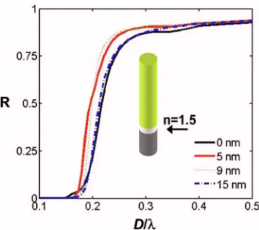
We now consider the metallic post mirror geometry sketched in the inset of Fig. 3. Such mirrors might
Fig. 2. (Color online) Performance of facets connecting with a silver substrate. (a) HE11 modal reflectance on a planar silver mirror either bare (t = 0, solid curve) or covered by a thin dielectric adlayer共n=1.5兲 of thickness t 共=950 nm兲 (b) Longitudinal cross section for the y compo-nent of the magnetic-field pattern for D /=0.19 and t=0 共R=0.3%兲, showing a self-focusing effect at the nanowire– silver interface, where 15% of the incident HE11energy is absorbed.
prove more compact and versatile than planar ones. Figure3 shows the facet reflectance as a function of
D / for several adlayer 共n=1.5兲 thicknesses. As
ex-pected, low reflectance is always observed for small diameters due to the weak interaction between the metallic post and the HE11field that is weakly con-fined. However, interestingly, the post geometry
of-fers high reflectance 共R⬎80%兲 for D⬎0.26 (black
solid curve), or even for D⬎0.22 (dotted green
curve) provided that a 9 nm thick adlayer is inserted at the GaAs–gold interface. For this optimal thick-ness, 0.9 reflectance is achieved for D as small as 0.28. The computational results in Fig. 3 are ob-tained for a semi-infinite metal post, but virtually identical results have been obtained for 100 nm thick posts, letting us expect a similar reflectance for gold-coated facets in freestanding nanowires. We have also studied the performance of the planar and post mirror at=1500 nm using either gold or silver. Re-sults similar to those in Figs. 2and 3 have been ob-tained for both metals.
We are currently investigating the planar–mirror fabrication by depositing the adlayer and the metal film onto a planar GaAs wafer incorporating a sacri-ficial GaAlAs layer. Then wafer bonding techniques are used to stick the sample upside down on another substrate, and the nanowire is finally processed by standard e-beam lithography and reactive ion etch-ing. The post geometry can be further obtained by us-ing an additional ion beam etchus-ing step. It can also be fabricated by direct thin film deposition onto a cleaved facet. Note that quite similar geometries are
also obtained when gold droplets are used as cata-lysts to assist nanowire growths [16]. Such mirrors could improve the efficiency of single-photon sources or could be incorporated to reduce the laser threshold of elementary nanowire resonators, offering quality factors of ⬃100 for first-order Fabry–Perot reso-nances.
The authors gratefully acknowledge fruitful discus-sions with G. Lecamp and B. Gayral. The work has been performed under the NanoEPR project of the 2006 NanoSci-ERA European program.
References
1. X. F. Duan, Y. Huang, R. Agarwal, and C. M. Lieber, Nature (London) 421, 241 (2003).
2. J. C. Johnson, H. Q. Yan, P. D. Yang, and R. G. Saykally, J. Phys. Chem. B 107, 8816 (2003).
3. M. T. Hill, Y. S. Oei, E. Smalbrugge, Y. Zhu, T. De Vries, P. J. van Veldhoven, F. W. M. van Otten, T. J. Eijkemans, J. P. Turkiewicz, H. De Waardt, E. J. Geluk, S. H. Kwon, Y. H. Lee, R. Nötzel, and M. K. Smit, Nat. Photonics 1, 589 (2007).
4. B. Z. Tian, X. L. Zheng, T. J. Kempa, Y. Fang, N. F. Yu, G. H. Yu, J. L. Huang, and C. M. Lieber, Nature (London) 449, 885 (2007).
5. Y. K. Lize, E. C. Magi, V. G. Ta’eed, J. A. Bolger, P. Steinvurzel, and B. J. Eggleton, Opt. Express 12, 3209 (2004).
6. M. T. Borgström, V. Zwiller, E. Müller, and A. Imamog˘lu, Nano Lett. 5, 1439 (2005).
7. Y. R. Nowicki-Bringuier, R. Hahner, J. Claudon, G. Lecamp, P. Lalanne, and J. M. Gérard, Ann. Phys. (Paris) 32, 151 (2008).
8. A. W. Snyder and J. D. Love, Optical Waveguide Theory (Chapman and Hall, 1983).
9. J. P. Hugonin and P. Lalanne, J. Opt. Soc. Am. A 22, 1844 (2005).
10. For a radial dipole, the fraction of the dipole emission that is coupled in the fundamental HE11 mode may exceed 90% for D /=0.23; see D. Y. Chu and S. T. Ho, J. Opt. Soc. Am. B 10, 381 (1993).
11. G. Lecamp, P. Lalanne, and J. P. Hugonin, Phys. Rev. Lett. 99, 023902 (2007).
12. L. Chen and E. Towe, Appl. Phys. Lett. 89, 053125 (2006).
13. G. Lecamp, J. P. Hugonin, P. Lalanne, R. Braive, S. Varoutsis, S. Laurent, A. Lemaître, I. Sagnes, G. Patriarche, I. Robert-Philip, and I. Abram, Appl. Phys. Lett. 90, 091120 (2007).
14. E. D. Palik, Handbook of Optical Constants of Solids (Academic, 1985), Part II(1).
15. P. Lalanne, J. P. Hugonin, and J. C. Rodier, J. Opt. Soc. Am. A 23, 1608 (2006).
16. P. J. Pauzauskie and P. Yang, Mater. Today 9, 36 (2006).
Fig. 3. (Color online) HE11modal reflectance of facets con-necting with a silver post (inset) for several values of the adlayer 共n=1.5兲 thickness t=0, 5, 9, and 15 nm 共 = 950 nm兲.