HAL Id: tel-01931367
https://tel.archives-ouvertes.fr/tel-01931367
Submitted on 22 Nov 2018
HAL is a multi-disciplinary open access archive for the deposit and dissemination of sci-entific research documents, whether they are pub-lished or not. The documents may come from teaching and research institutions in France or abroad, or from public or private research centers.
L’archive ouverte pluridisciplinaire HAL, est destinée au dépôt et à la diffusion de documents scientifiques de niveau recherche, publiés ou non, émanant des établissements d’enseignement et de recherche français ou étrangers, des laboratoires publics ou privés.
for TiO2- and ZnO- based Solid-State Dye-Sensitized
Solar Cells (s-DSSCs).
Annette Delices
To cite this version:
Annette Delices. Organized Organic Dye / Hole Transporting Materials for TiO2- and ZnO- based Solid-State Dye-Sensitized Solar Cells (s-DSSCs).. Other. Université Sorbonne Paris Cité, 2017. English. �NNT : 2017USPCC066�. �tel-01931367�
Thèse de doctorat
de l’Université Sorbonne Paris Cité
Préparée à l’Université Paris Diderot
Ecole doctorale de Chimie Physique et de Chimie Analytique de
Paris-Centre (ED 388)
Laboratoire Interfaces Traitements Organisation et Dynamique des Systèmes
Organized Organic Dye / Hole Transporting
Materials for TiO
2
and ZnO based
Solid-State Dye-Sensitized Solar Cells (s-DSSCs)
Par Annette DELICES
Thèse de doctorat de Chimie
Dirigée par Pr. Mohamed JOUINI
Présentée et soutenue publiquement à L’Université Paris Diderot le 29/09/2017
Président du Jury : Pr. MAUREL François, Professeur, Université Paris Diderot Rapporteurs : Dr. FABRE Bruno, Directeur de Recherche, Université de Rennes
Dr. GUILLEMOLES Jean-François, Directeur de Recherche, IRDEP Examinateurs : Pr. LARTIGAU-DAGRON Christine, Professeur, Université de Pau Dr. MOINEAU-CHANE CHING Kathleen, Directrice de Recherche, Université de Toulouse
Co-directeur de thèse : Pr. HAGFELDT Anders, Professeur, Ecole Polytechnique Fédérale de Lausanne – Suisse
state DSSCs (s-DSSCs). Among them, the substitution by conducting polymers (CP) has attracted considerable attention because of their good stability, high hole-conductivity and simple deposition within the mesoporous TiO2 semiconductor. In this thesis work, several s-DSSCs based on CPs used as HTM have
been developed in order to improve their photovoltaic performances taking into account the following two objectives: (i) the optimization of the interfacial charge transfer processes within the solar cell, and (ii) the optimization of the charge transport within the n-type oxide semiconductor. To reach these goals, each component that constitutes the device was varied in order to investigate its effect on the device’s performances. As first attempt, an analytical study is carried out by varying the sensitizer in order to determine the fragments of the dyes structures, that have an important effect on the in-situ photo electrochemical polymerization process (PEP) both in organic and in aqueous media and hence on the performances of the s-DSSCs. Based on these results, a new concept of removing completely the interface between the dye and the HTM is developed. This is achieved by the synthesis of new dyes covalently linked to an electroactive monomer which is co-polymerized by in-situ PEP. The resulting co-polymer, used as HTM, is covalently linked to the dye. In addition, the nature of the chemical bond linking the triphenylamine residue TPA to the monomer is also investigated as a key factor in the s-DSSCs performances. Besides, and to optimize the charge transport processes within this type of s-DSSC, the elaboration of novel ZnO based s-DSSCs has been achieved and investigated.
Keywords: Solid-State Dye-Sensitized Solar Cells, in-situ Photo- Electrochemical Polymerization, donor-linker-acceptor organic dyes, covalent link, hole transporting material, conducting polymer, TiO2, ZnO.
Résumé
En raison des problèmes d'instabilité à moyen termes des cellules solaires à colorant (DSSC), l'électrolyte liquide à base d'iodure a été remplacé par plusieurs types de matériaux solides transport de trous (HTM) pour obtenir des DSSCs à l'état solide (s-DSSCs). Parmi ces matériaux, l’utilisation des polymères conducteurs (PC) a attiré une attention considérable en raison de leur bonne stabilité, de leur haute conductivité et de la facilité de leur dépôt sur le semi-conducteur mésoporeux TiO2. Dans ce travail de thèse, plusieurs s-DSSCs
basées sur des PC utilisés comme HTM ont été développés dans le but d'améliorer leurs performances photovoltaïques en tenant compte des deux objectifs suivants: (i) l'optimisation des processus de transfert inter facial de charge dans la cellule solaire, et (ii) l'optimisation du transport de charge dans le semi-conducteur d'oxyde de type n. Pour atteindre ces objectifs, chaque composant de la s-DSSC a été modifié afin d'étudier son effet sur les performances du dispositif final. En première tentative, une étude analytique est réalisée en faisant varier le sensibilisateur afin de déterminer les fragments de la structure du colorant, qui ont un effet important sur le processus de photopolymérization électrochimique in-situ (PEP) à la fois en milieu organique et en milieu aqueux mais aussi sur les performances des s-DSSCs. Sur la base de ces résultats, un nouveau concept a été développé et consiste en la suppression totale de l'interface entre le colorant et le HTM. Ceci est obtenu par la synthèse de nouveaux colorants liés de façon covalente à un monomère électroactif qui est co-polymérisé par la PEP in-situ. Le copolymère résultant, utilisé comme HTM, est lié de manière covalente au colorant. En outre, la nature de la liaison chimique, reliant le résidu triphénylamine TPA au monomère, est également étudiée comme un facteur clé dans les performances de s-DSSC. En outre, et pour optimiser les processus de transport de charges dans ce type de s-DSSC, de nouvelles s-DSSC basées sur ZnO ont été réalisées et étudiées.
Mots-clés: Cellules solaires à colorant solide, photopolymerization électrochimique in-situ, colorants organiques donneur-accepteur, liaison covalente, matériaux transporteur de trous, polymère conducteur, TiO2, ZnO.
Abbreviations
ACN Acetonitrile
ALD atomic layer deposition
BL blocking layer CB conduction band CBZ carbazole CE counter electrode CP conducting polymer CV cyclic voltammetry
CVD chemical vapor deposition
DCM dichloromethane
DEA diethanolamine
DFT density functional theory
DSSCs dye-sensitized solar cells
D-π-A Donor – Linker – Acceptor
EDOT 3,4-ethylenedioxythiophene
EF Fermi level
EG Bandgap energy
Eonset,ox onset of the oxidation potential
Eox (dye) oxidation potential of the dye
EPD electrochemical deposition
EQ-F quasi-Fermi level
ETM electron transporting material
FF fill factor
FTO fluorine doped tin oxide
HRMS High resolution mass spectrum
HTM hole transporting material
ic capacitive current
ICT intramolecular charge transfer
if faradic current
IPCE Incident Photon-to-Electron Conversion Efficiency
ITO indium doped tin oxide
J current density
Jsc short-circuit current density
LCAO linear combinations of atomic orbitals
LiTFSI Li(CF3SO2)2N
Ln electron diffusion length
NR nanorods
OFETs organic field-effect transistors
OLEDs organic light-emitting diodes
OPV Organic Photovoltaic
PANI polyaniline
PCE power conversion efficiency
PEDOT poly (3, 4-ethylenedioxythiophene)
PEN polyethylene naphthalate
PEP (in-situ) photo-electrochemichal polymerization
PET polyethylene terephthalate
PIA photoinduced absorption spectroscopy
Pin the incoming power
PPy polypyrrole
PVD physical vapor deposition
RCT charge transfer resistance
RE reference electrode
SCE saturated calomel electrode
SCN thiocyanato
s-DSSCs solid-state DSSCs
SHE standard hydrogen electrode
SNS 2,5-di(thiophen-2-yl)-1H-pyrrole
TBP 4-tert-butylpyridine
TCO transparent conducting oxide
TDDFT time dependent DFT
TPA triphenylamine
VB valence band
Voc open circuit potential
WE working electrode
η efficiency
Contents
General Introduction ... 1
Chapter I From Fossil Fuel to Renewable Energy: The Emergence of Solar Cells in Energy Transition ... 3
I. 1. Photovoltaic effect: generalities ... 5
I. 1. a. The Sun: Primary Source of Energy ... 5
I. 1. b. Basic principle of photovoltaic ... 7
I. 1. c. Solar Cells: The Three Generations ... 12
I. 2. DSSC: Structure and components ... 16
I. 2. a. The photo-anode ... 17
I. 2. b. The photo-sensitizer ... 22
I. 2. c. The Hole Conducting Material ... 31
I. 2. d. The Counter Electrode ... 36
I. 3. Solid State-DSSC: operating principle and photovoltaic performances ... 37
I. 3. a. The Operating Principle ... 39
I. 3. b. Excitation, Electron Injection, Electron Transport and Charge Recombination ... 40
I. 3. c. Solar Cell Performances ... 43
I. 4. Aim of the thesis ... 47
I. 5. References ... 49
Chapter II Influence of D-π-A Organic Dyes Structures on TiO2 based s-DSSCs Performances ... 59
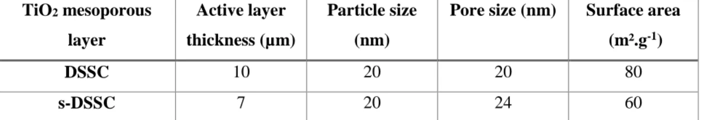
II. 1. Generalities and Material used in s-DSSCs ... 60
II. 1. a. TiO2 Photo-anode: Preparation Methods ... 60
II. 1. b. LEG4, D35, L1, BA504, BA741 and RK1 D-π-A Organic Dyes Structure Overview and Sensitization Step ... 62
II. 1. e. Additives ... 73
II. 1. f. Counter-electrode ... 74
II. 2. Experimental Section ... 74
II. 2. a. Preparation of the TiO2 Photo-anode ... 74
II. 2. b. Sensitization Step: Dye Adsorption ... 76
II. 2. c. The In-situ Photo-Electrochemical Polymerization Process of Conducting Polymers . 76 II. 2. d. Additives and Counter Electrode ... 77
II. 3. Results and Discussion ... 78
II. 3. a. Characterization of the TiO2 Photo-anode ... 78
II. 3. b. Properties of LEG4, D35, L1, BA504, and BA741 Dyes ... 80
II. 3. c. Study of in-situ PEP using L1, D35, LEG4, RK1, BA504 and BA741 organic dyes ... 87
II. 3. d. Characterization of PEDOT layer in-situ produced on the dyed photo-anode ... 92
II. 3. e. s-DSSCs devices performances ... 94
II.4. Conclusion ... 101
II. 5. References ... 102
Chapter III Effect of the Dye-HTM Covalent Link on s-DSSCs Performances ... 106
III. 1. Optimization of the Interfacial Charge Transfer ... 107
III. 1. a. General context ... 108
III. 1. b. Novel Organic Dyes Covalently Linked to the CP generated by in-situ PEP ... 109
III. 2. Experimental details ... 113
III. 2. a. ADCBZ and ADSNS Dyes Synthesis ... 113
III. 2. b. Characterization Techniques for Dyes Structure and Dye-Sensitized TiO2 Substrates ... 114
III. 2. c. In-situ PEP process and s-DSSC performances ... 115
III. 3. Results and Discussion ... 115
III. 3. c. s-DSSCs devices performances ... 123
III. 3. d. Discussion ... 126
III. 3. e. Impact of the s-DSSCs aging process on photovoltaic performances ... 127
III. 4. Conclusion ... 128
III. 5. References ... 130
Chapter IV Influence of the Nature of the Covalent Link between the Dye and the HTM on s-DSSCs Performances ... 132
IV. 1. Modification of the covalent link between the dye and the HTM ... 133
IV. 1. a. General context: extension of electron donating in the donor part ... 134
IV. 1. b. Proposed organic dyes containing the electroactive monomer ... 135
IV. 2. Experimental details ... 137
IV. 2. a. Preparation of building blocks ... 137
IV. 2. b. Preparation of ADCBZ-1, ADSNS-1, ADCBZ-2 and ADSNS-2 dyes ... 138
IV. 3. Results and Discussion ... 139
IV. 3. a. Dyes syntheses and physico-chemical characterization ... 140
IV. 3. b. In-situ PEP deposition of PEDOT on the Sensitized TiO2 Photo-anodes ... 148
IV. 3. c. s-DSSCs devices performances ... 150
IV. 3. d. Impact of the s-DSSCs aging process on photovoltaic performances ... 153
IV. 3. e. Discussion ... 154
IV. 4. Conclusion ... 155
IV. 5. References ... 156
Chapter V Modification of the Oxide Semiconductor in s-DSSCs: Use of ZnO ... 157
V. 1. Optimization of the Electron Transport Process within the Semiconductor ... 158
V. 1. a. General context ... 159
V. 1. b. s-DSSCs based ZnO using Conducting Polymers generated by in-situ PEP ... 162
V. 2. b. Preparation of ZnO mesoporous layer ... 165
V. 2. c. Sensitization Step: Dye Adsorption ... 166
V. 2. d. In-situ PEP process and additives ... 166
V. 2. e. Characterizations and s-DSSC performances ... 166
V. 3. Results and Discussion ... 167
V. 3. a. Electrochemical characterization of the ZnO blocking layer ... 167
V. 3. b. Structural characterization of ZnO blocking layer and ZnO mesoporous layer... 170
V. 3. c. Characterization of D35 dye sensitized ZnO photo-anode ... 173
V. 3. d. In-situ PEP using D35 organic dye in organic medium ... 175
V. 3. e. SEM characterization of FTO/ZnO/D35/PEDOT photo-electrode ... 176
V. 3. f. ZnO based s-DSSCs devices performances ... 177
V. 3. g. Discussions ... 179
V. 4. Conclusion ... 180
V. 5. References ... 181
General Conclusion and Perspectives ... 183
Annex I ... 187
Annex II ... 188
Annex III ... 194
1
General Introduction
Fossil fuels including coal, natural gas and oil are at present the world’s primary energy sources which contribute to the greenhouse effect and thus to the global warming. This global warming is currently causing temperature and sea level rises, extreme weather phenomena (such as heavy rainfall, drought or storms) and a decline in agriculture yields, thus threatening mankind, biodiversity and our planet. With the objective to limit global warming below the 2 °C, agreement approved during the annual Conference of Parties - COP21, leaders from all parties progress toward a 100 % renewable energies future. The EU countries have already set themselves a target of 27 % final energy consumption from renewable sources by 2030.
Solar energy is the most promising renewable energy source since it is usable on the whole planet. Solar thermal energy and photovoltaics are two different technologies, both exploiting the sun as an energy source. The photovoltaic principle is the direct conversion of sunlight into electricity through modules known as solar cells. Photovoltaic technology has particularly attracted great interest as a sustainable, cost-effective device exhibiting high efficiency with much lower CO2 emission. To date, the top-performing solar cell sits at 46 %: it is made of III-V
compound semiconductor materials also known as multi-junction solar cells. Recently, researchers at the Fraunhofer Institute have successfully manufactured a silicon-based multi-junction solar cell with a record conversion efficiency of 30.2 %. Silicon is at present the basic component in conventional solar cells that currently dominates the world market. However, emerging photovoltaic technologies, such as perovskite, organic (OPV), tandem, quantum dots (QDSCs) and dye-sensitized solar cells (DSSCs), provide comparable efficiency both at low-cost manufacturing and using cost-effective starting materials, thus moving these technologies toward industrial production. They are becoming potentially competitive with silicon solar cells.
Classified in the third generation category of photovoltaics and known as “Grätzel cells”, the interest for DSSCs began in 1991, since Michael Grätzel and Brian O’Regan reported the first cell: partially inspired by photosynthesis process, it recorded a solar efficiency at 7 %. The most powerful DSSC has been developed by K. Kakiage et al. in 2015 and now reaches 14 % efficiency. Despite their attractive properties and compared to the other emerging photovoltaic technologies, DSSCs are built from eco-friendly, colorful and semi-transparent constituent
2 of a photoanode, made of a mesoporous TiO2 semiconductor coated with the dye, a
counter-electrode and a liquid electrolyte, which contains triiodide and iodide redox shuttle (I3-/ I-) used
as hole transporting material (HTM) for the regeneration of the sensitizing dye molecule. Nowadays, most of the present researches on DSSCs are focused on optimizing each component, in order to further improve the device performances and durability.
Due to instability problems in longtime uses the iodine based liquid electrolyte has been replaced by several types of solid HTMs, namely in solid-state DSSCs (s-DSSCs). Among them, the substitution by a p-type conducting polymer (CP) has attracted considerable attention because of its good stability, high hole-conductivity and its simple deposition within the mesoporous TiO2
semiconductor. In this thesis work, several s-DSSCs based on CPs used as HTM have been developed in order to improve their photovoltaic performances taking into account the following two objectives:
(1) Optimizing the interfacial charge transfer processes within the solar cell (2) Optimizing the charge transport within the n-type oxide semiconductor.
Therefore, two different approaches were attempted in these s-DSSCs with the aim to give them a real sustainability and stability without neglecting the ecological and economic aspects. The first approach is the design of innovative organic donor-acceptor dyes with a new concept consisting in the total removal of the interface between the dye and the HTM, and the second is the substitution of the TiO2 semiconducting material by ZnO.
Chapter I
From Fossil Fuel to Renewable Energy:
4 With the rapid growth of the global population that will arise in very near future, the world energy demand is expected to increase to an unprecedented pace. Fossil fuels are at present the primary energy source supplying more than 80 % of the world energy consumption. However, these non-renewable resources are pollutants and becoming scarce. In fact, according to the International Energy Agency report[1,2], the world energy production reached 13700 Million Tonnes of Oil Equivalent (Mtoe) in 2014 including oil (31 %), coal (29 %), natural gas (21 %) and nuclear (5 %). At this current rhythm of production, the world energy reserves are expected to be exhausted within 84 years on average[3]. In a world dependent on these resources for transport, industry, housing or electricity; safeguards become a primary concern for all States of the world at the economic and political levels (Kyoto Protocol, Energy Transition). This leads to the development of new and innovative technologies based on non-fossil sources, known as renewable energies, for a more-efficient and a more-carbon free energy production and consumption. Renewable energy technologies produce sustainable energy from sun, wind, water and plants, and presently amount to 14 % of the world energy production (Figure I-1).
Figure I-1: Total primary energy supply by fuel in 2014 [2]
In recent years, the amount of energy produced by photovoltaic technology has increased considerably while the market price has diminished, enabling solar energy to be both more accessible for the realization of projects and increasingly competitive relative to other energy sources reaching progressively all countries of the world including emerging countries (China, India). The development prospects of solar energy industry are therefore promising and will play an essential role in the energy transition under the Kyoto Protocol. Chemistry is the heart of this technological breakthrough allowing the development of different types of novel solar cells from a variety of innovative materials.
5
I. 1.Photovoltaic effect: generalities
The photovoltaic effect, “Photo” from the Greek meaning light and “voltaic” for the electric potential pioneered by Alessandro Volta, is a process in which two dissimilar materials in close contact produce an electrical voltage when struck by light or other radiant energy[4]. In most
photovoltaic applications the radiant energy comes from the sunlight. It is therefore essential to understand the photovoltaic operating principle and to have an overview on the composition of the solar spectrum that drove researchers to develop a multitude of solar cells.
I. 1. a. The Sun: Primary Source of Energy
The global world energy consumption, in 2014, amounts to 9425 Mtoe or approximately 109 613 TWh from all sources[5]. 19.2 % of our energy consumption originates from renewable energy
and only 0.2 % of it, is generated by solar energy which translates in power into 190.8 TWh[6]
that means 106 times less than the annual solar energy power received by the Earth (109 TWh)[7]. Therefore the Sun is, in itself, a useable energy source. Indeed, knowing that the luminosity of the Sun is 3.846 X 1026 W and the distance from Earth to the Sun is 1 astronomical unit (A.U.) i.e. 1.496 X 10¹¹ m, the solar constant i.e. the flux of solar radiation that receives a surface of 1 m² at the top of the Earth in zero atmosphere, is roughly 1360 W/m². It should however be pointed out that this solar constant is estimated above Earth’s atmosphere exposed perpendicularly to Sun’s rays and varies +/- 3 % due to its elliptical orbit around the Sun.
Figure I-2: Spectral distribution of solar radiation of an ideal black body, at the top of the Earth’s atmosphere on the 37° inclined surface and at sea level taken from ref. [8].
6 Solar radiation issued by the visible surface of the Sun, namely photosphere, refers to the electromagnetic radiation with a spectral distribution ranging from 0.2µm to 2.6 µm, fairly similar to the black body radiation spectrum at a 5800 K[9] (Figure I-2). This electromagnetic
radiation, including gamma rays, X-rays, Ultra-Violet, visible, Infra-Red, microwaves and radio waves, can be described (wave-particle duality) in terms of electromagnetic wave characterized by a frequency ν and a wavelength λ, and also of massless stream of particles, known as photons, moving at speed of light in vacuum (c= 3.108 m.s-1). The energy of this elementary particle is given by the Planck-Einstein relation:
𝐸 = ℎ𝜈 = ℎ𝑐
𝜆 (I-1)
With the Planck’s constant h= 6.6 x 10⁻³⁴ J.s
However, not all of the electromagnetic radiation reaches the Earth’s surface: some parts of this radiation are attenuated when it crosses the atmosphere. This electromagnetic radiation is, in fact, disturbed both by scattering and absorption processes due to gas molecules, aerosols, clouds that mainly constitutes the Earth’s atmosphere. The solar spectrum at Earth’s surface is therefore
dependent of many atmospheric
parameters as well as the path length
through the atmosphere. It is
characterized by an Air-Mass
coefficient, “AM X”, and defined as the optical path length L through Earth’s atmosphere. When the Sun is directly at its zenith (θ= 0°) the Air-Mass indicator is denoted AM 1, “1” for one atmosphere with a solar irradiance at Earth’s surface (at sea level more precisely) reaching 1040 W/m² in optimum conditions. This value is further reduced compared to the extraterrestrial solar radiation referred as
Figure I-3: Air-Mass coefficient depiction at 0, 1, and 1.5 atmospheres.
7 air mass zero, AM 0, meaning no atmosphere, and with a solar irradiance equivalent to the solar constant (Figure I-3).
For incident solar radiation at angle θ relative to the normal to the Earth's surface L0, the
Air-Mass coefficient is expressed as:
𝐴𝑀 𝑋 = 𝐿
𝐿0
= 1
𝑐𝑜𝑠 𝜃 (I-2)
AM 1.5 is the standardized solar spectrum, established by the American Society for Testing and Materials (ASTM), corresponding to a zenith angle of θ= 48.2° (according to the tilt angle at 37° toward the equator) commonly used for terrestrial applications such photovoltaic solar cells. The power density related to AM 1.5G (G for a global radiation) is estimated at 1000 W/m² at room temperature[10], used as reference in this thesis work.
I. 1. b. Basic principle of photovoltaic
The photovoltaic effect, discovered in 1839 by the French physicist Alexandre Edmond Becquerel, is a property that some materials exhibit to produce electricity when exposed to the light. From his experiments, A. E. Becquerel highlights the production of voltage and current, within an electrochemical cell consisting of silver chloride electrode connected to a counter platinum electrode dipping in an acidic electrolytic solution, when exposed to light[11]. During the following 100 years, research in photovoltaic field have intensified and mainly well described by Albert Einstein on his 1905 paper[12] behind “photoelectric effect” for which he won the Nobel Prize. Based on these works, in 1954 researchers from Bell Laboratories developed the first concrete solar cell, relatively efficient to convert enough solar energy into electric power with efficiency of 6 %. This principle is only based on semiconductor technology made from crystalline silicon, basic component that currently dominates the market. In fact, Russell Ohl from Bell Labs inadvertently discovered in 1940 that doped silicon, arising from the combination of a p-type semiconductor (p for positive charges) and an n-type semiconductor (n for negative charge), produced a flow of electricity under light irradiation. The resulting p-n junction is required to get an energy conversion from photons to electrons. To be able to explain the operating principle of a photovoltaic cell, we will first review the photovoltaic concept in
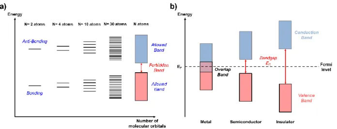
8 quantum chemistry and in solid-state physics. According to the valence bond theory, only electrons of the valence shell, the outermost shell from the nucleus, are engaged in a covalent bond in a molecule. The chemical bonding can also be described following the molecular orbital theory as linear combinations of atomic orbitals (LCAO). An orbital is a wave function Ψ describing the state of an electron depending on the distance from the nucleus (r) and the angle (θ, φ) which is the solution of the Schrödinger equation. The square modulus of this wave function |Ψ|2 is the probability of finding the electron in a space around a single atom
(i.e. hydrogen). By solving |Ψ|2, the wave function, described upon three quantum numbers: n (principle), l (angular), and m (magnetic), corresponds to the atomic orbital (1s for H) with an energy value determined exclusively from n. For a diatomic molecule, H2 for example, the
covalent bond between two H atoms resulting from the overlap of 2 atomic orbitals (AO), following the LCAO leads to 2 coupled levels, 2 molecular orbitals (MO) with no more than 2 electrons per orbital, each distinguished by their spin (Pauli exclusion principle). One is referred to the “bonding” MO of lower energy (from the 2 AO constructive interference), and the other is called “anti-bonding” MO of higher energy (from the 2 AO destructive interference). Similarly, if we apply to larger molecules comprising N atoms, such as crystal lattice, each of their AO overlap with AO of the N-1 other atoms leading to an infinite number of MOs at different energy levels. They are so close that they form a continuum of energy levels as an energy band (Figure I-4a)). The latter is equivalent to the electronic band structures in solid-state physics. Indeed, due to the periodic array of atoms, electrons feel the presence of other electrons through the periodic potential. Each of these new wave-functions ascribed to electrons by solving the Schrödinger equation is the Bloch’s wave introduced by the Physicist Felix Bloch during his doctoral thesis[13]. Similarly, each wave-function associated to an energy gives rise to a
denumerable set of electron states as quasi-continuous bands known as “allowed bands” each separated by a “forbidden band”.
From this electronic band structure, materials can be classified upon their electrical conductivity. At 0 K, the energy levels are filled by electrons starting from the lowest. The levels that are filled by electrons constitute the valence band (VB). Beyond this band, the first lowest vacant band is the conduction band (CB). The Fermi level (EF), lying between the valence and the conduction
band, refers to the chemical potential of electrons. For metals, the valence and conduction band overlap without any additional energy. Such metals contain a large number of free electrons and
9 hence are highly conductive (Figure I-4b)). When these two bands are separated by a forbidden band called “bandgap” (EG), the material is either an insulator or a semiconductor. In the case of
insulator, the bandgap is high, thus it is impossible for an electron to jump from the VB to CB, even at room temperature (RT), and hence it cannot conduct. By contrast, for semiconductors the bandgap is sufficiently narrow to lift an electron from VB to CB at RT, leaving at the same time a hole in the VB. This hole in the VB is ultimately assimilated to positive charge that carries the current. They are thus conductive. These created electron-hole pairs are charge carriers corresponding to excitons[14].
Figure I-4: a) Molecular orbital energy level diagram for 2, 4, 10, 30 and N atoms. b) Schematic band diagram for metal, semiconductor and insulator.
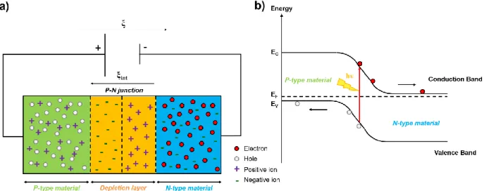
To make a semiconductor more conductive few electrons are included in the CB or, in an equivalent manner, some electrons from the VB are removed: this is the “doping” process. The terms used to specify a doped semiconductor (extrinsic) with an excess of electrons or holes, assimilated as impurities or defects, are n-type or p-type semiconductor respectively. Depending on the doping process, the Fermi level will be obviously impacted. For n-type semiconductor, the Fermi level shift toward the CB or toward the VB for the p-type semiconductor. When these two doped n-type and p-type semiconductors are joined, the p-n junction is formed. Some electrons from the n region diffuse across the junction to reach the p region leaving an ionized donor behind. Similarly, holes from the p region diffuse to n region leaving behind an ionized acceptor. Thus a new region, depleted on free charge carriers, is created in the vicinity of the junction resulting from the electrons-holes diffusion and recombination: this is the depletion zone. Furthermore, the presence of ions (negative in p region and positive in n region) generates an
10 electric field across the junction and causes the separation of electrons and holes and their transfer in the opposite direction to the diffusion process. When the electric field compensates the diffusion it leads to an equilibrium state. If an external field is applied by means of generator by connecting the + pole to the p region and – pole to the n region, it creates an electric field ξ in reverse direction to the internal field ξint (or built-in electric field), this is the forward bias and as
a result the charge carriers flow and the current is obtained (Figure I-5a). The standard device having this configuration and relying on this operating principle is a diode.
Figure I-5: a) P-N single junction diode under forward bias. b) Energy band diagram of a solar cell P-N junction.
The current flow is also obtained from the illumination of the p-n junction: this is the photovoltaic effect. When the junction is illuminated, a photon is absorbed by the semiconductor by stripping an electron from its VB to the CB provided that the energy of the photon is greater than the bandgap energy (Figure I-5b)). The generated exciton located in the depletion zone, where the internal electric field takes place, splits up and the electron moves toward the n side unlike the hole pushed toward the p side. The electron joins the hole through the external connection giving rise to a difference of potential: the electric current flows. The photovoltaic cells are then assembled to form modules.
As mentioned above, the most dominant semiconductor material used for photovoltaic technology is crystalline silicon. The choice of silicon (Si) atom is supported by the presence of 4 valence electrons (group IV) allowing to be covalently bonded with 4 neighboring Si atoms (tetravalent) resulting in a diamond cubic crystal structure in the crystal lattice. If one atom of Si is replaced by an atom of the group V, commonly phosphorous (P), the semiconductor is n-doped
11 due to the excess of free electrons. However, if Si is replaced by an atom of the group III, boron for example, the semiconductor is p-doped, due to the presence of holes.
Hence, the p-n junction is achieved. The energy bandgap as well as its light absorption ability of a semiconductor must be taken into consideration. The energy bandgap of semiconductors depends on the temperature following the relation proposed in 1967 by the physicist Y. P. Varshni[15] :
𝐸𝐺(𝑇) = 𝐸𝐺(0) − 𝛼 𝑇
2
𝑇 + 𝛽 (I-3)
Where EG is the energy bandgap which may be direct (same crystal momentum p⃗ for CB et VB)
or indirect (different crystal momentum p⃗ for CB et VB), EG(0) is the energy bandgap at 0 K, α
and β are constants related to the material. Table I-1 provides the bandgap energy of homojunction (Si, Ge) and of heterojunction (GaAs) semiconductors[16,17].
Material Bandgap EG (0) α (eV/K) β (K) EG (300 K)
Si 1.170 eV 4.73 x 10⁻⁴ 636 1.12 eV
Ge 0.7437 eV 4.77 x 10⁻⁴ 235 0.66 eV
GaAs 1.519 eV 5.41 x 10⁻⁴ 204 1.42 eV Table I-1: Bandgap energy of Si, Ge, and GaAs semiconductors at 0K and 300K.
For Si the energy bandgap is 1.12 eV at RT, so the photons must have an energy value higher than 1.12 eV or 1.79 x 10⁻¹⁹ J. In wavelength, Si semiconductor will absorb a large portion of the
spectrum till the cut-off wavelength λG from 1100 nm to 250 nm.
𝜆𝐺(𝑛𝑚) =
ℎ × 𝑐
𝐸𝐺 × 1.6 × 10−28 =
1242
𝐸𝐺 (I-4)
Beyond 1100 nm, photons are not absorbed and pass through the cell (18 %). This is one of the reason why Si solar cell is not 100 % efficient. Another reason is that almost the half of the sun irradiance is re-emitted as heat or light. Theoretically, 32 % of the sunlight can be converted as electricity with Si according to the “Shockley-Queisser limit” computations performed by W. Shockley and H.J. Queisser in 1961[18]. The predicted maximum efficiency is 33.7 % assuming single junction semiconductors with an energy bandgap of 1.34 eV (Figure I-6).
12 Figure I-6: Comparison between the most efficient single junction solar cells with the fundamental Shockley-Queisser limit
(black line). The figure is taken from ref. [19] and AMOLF.
At present, the best efficiency for a single junction cell reaches 28.8 % close to the theoretical value. The cell was developed in 2012 by Alta Devices based on gallium arsenide (GaAs) which is an III-V heterojunction semiconductor[20]. Compared to Si and Ge, GaAs has the benefit of being a direct bandgap material. The nature of the gap has a fundamental role in the interaction of the semiconductor with electromagnetic radiation. In the case of a direct bandgap semiconductor, the electron characterized by a wave vector k⃗ passes from the VB to the CB without changing the momentum (p⃗ = ħ k⃗ ) and whose energy is equivalent to EG. In the indirect bandgap
semiconductor, the momentum is larger.
Remarkable progresses have been achieved in the field of photovoltaic, by the development of new solar cells such as multijunction cells, thin film technologies and emerging photovoltaics.
I. 1. c. Solar Cells: The Three Generations
In the field of photovoltaic, research and development generally aims to provide higher efficiency and lower costs per watt of electricity generated for large scale application. In some countries, the production cost of electricity from solar energy is already lower than that of coal[21]. It is mainly produced by silicon solar cells classified in the first generation. Indeed, solar cells are usually identified in different "generations" according to the engineering of their architecture (Figure I-7).
13 Figure I-7: The different photovoltaic technologies divided into three generations followed by their highest efficiency.
Generally the first generation includes crystalline Si cells (c-Si) made of wafers, as mentioned above, that provide the highest efficiency in single junction solar cells. They differ by their allotropic form. When wafers are derived from a single silicon crystal and structure of the crystal is perfectly homogeneous, they refer to monocrystalline solar cells. For wafers composed of several silicon crystals of various and varied sizes, they refer to polycrystalline solar cells (Figure I-8). The former is known to be efficient and the latter to be easy to produce. However, for both, the processes used to improve the purity of silicon are expensive.
Figure I-8: Schematic representation of three allotropes of silicon (taken from the ref.[22]).
The purity is the limiting key factor that impact efficiency. Moreover the non-flexibility and the heaviness of silicon panels are two more issues that lead to the introduction toward thin-film technology.
Thin-film technology involves chemical vapor deposition technique and constitutes the second generation. The supporting substrate is made of cost-effective material such as glass, ceramic or plastic and it is thus lightweight. Thin-film solar cells are quite efficient and cheaper in
14 production to be sufficiently competitive to c-Si solar cells. The most successful thin-film technology is cadmium telluride (CdTe) solar cell patented by the American manufacturer First Solar[23]. CdTe belongs to the II-VI semiconductor group with a direct bandgap of 1.5 eV
allowing to get a high absorption coefficient. At present, CdTe solar cells have the lowest energy payback time (1 year) which refers to the time, measured in years, required for any photovoltaic system to produce as much energy as was required in its manufacture[24]. According to the National Renewable Energy Laboratory (NREL) the best efficiency is up to 22 % that makes them the second most dominant photovoltaic technology in the market. However, these cells contain cadmium which is a highly toxic element and its disposal and recycling are both are both risky and costly. Amorphous silicon (a-Si) (Figure I-7) and copper, indium, gallium, selenide (CIGS) are two alternative materials that are environmental friendly. The best efficiency for CIGS solar cells is comparable to CdTe with 22.3 % obtained by Japenese producer from Solar Frontier[25].
The third generation photovoltaics are the most promising technologies arising from the first generation and the second generation in terms of manufacture, flexibility, production cost, and toxicity. Devices are designed to overcome the Shockley-Queisser limit, for example by stacking multi-layers of single junction known as multi-junction solar cells. This is what Sharp Corporation achieved in 2009, by the development of a triple-junction solar cell combining three photo-absorption layers that have different bandgaps (Figure I-9).
Figure I-9: Spectral distribution of solar radiation and wavelength sensitivity of the three photo-absorption layers (taken from the ref. [26]).
15 The bottom, middle and top layers of the solar cell are made of InGaAs (0.97-0.99 eV), GaAs (1.43 eV) and InGaP (1.88 eV) respectively yielding to 37.9 %[27]. Similarly, the limit can also be
reached by stacking different solar cells so-called tandem solar cells that absorb optimally different part of the solar spectrum[28,29]. Researchers are also focused on innovative materials typically at nanoscale that deliver unique properties such as quantum dots[30,31] and yielded today at 11.5 %[32]. Quantum dots solar cells are part of emerging photovoltaic field[33] as well as plasmonic solar cells where the challenge is improving the light absorption due to the localized surface plasmon resonance[34]. The top performing of emerging photovoltaic is perovskite solar cell pioneered by the chemist T. Miyasaka in 2009[35]. Usually, a perovskite is in the form of ABX3 made of an organic cation (A), an inorganic cation (B) and an halogen anion (X) with a
bandgap of nearly 1.5 eV: so an efficient light harvester[36]. In their first report, Miyasaka et al. employed two methylammonium lead trihalide as perovskite nanocrystals: CH3NH3PbBr3 and
CH3NH3PbI3 with a bandgap of 2.02 eV and 1.44 eV respectively. Therefore CH3NH3PbI3 which
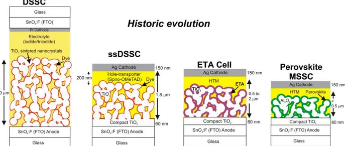
is more light-sensitive yielded an efficiency of 3.8 %. Since then, extensive research have been achieved and the highest efficiency reaches 22.1 %[37,38]. Historically, perovskite solar cells emerged from Dye-Sensitized Solar Cells (DSSCs) where the adsorbed dye has been replaced progressively by the perovskite[39] (Figure I-10).
Figure I-10: Emergence of perovskite solar cells starting from liquid state DSSC, then the electrolyte was replaced by a hole transporting material (Spiro-OMeTAD) followed by the replacement of the dye by an extremely thin absorber (ETA).
16 DSSC is one of the most developed third generation solar cells since the first implementation, conducted by M. Grätzel and B. O’Regan in 1991[40], has generated electricity from sunlight by
means of photosensitizers. The chemical process in DSSCs partially follows the natural process of photosynthesis standing out by far from others photovoltaic cells. In addition, the materials used are inexpensive, lightweight, semi-flexible, semi-transparent, environmental friendly and colorful, essential criteria well suited for both indoor and outdoor applications. In terms of efficiency, DSSCs display currently 14.3 %[41] which is relatively high considering their short energy payback time and their ease of production. Moreover, they are also performant at lower insolation level and under diffuse light. Therefore, they are a promising alternative to the dominant technology of silicon solar panels.
I. 2.DSSC: Structure and components
Conventionally, a DSSC is composed of four components: a photo-anode , a photoactive molecule , a hole conducting material and a counter electrode (Figure I-11). The photo-anode includes a metal semiconductor oxide layer deposited on a transparent conducting oxide (TCO) on a glass substrate or on plastic substrate. The photoactive molecule anchored to the mesoporous oxide semiconductor is a dye molecule which has the ability to harvest solar light. It is surrounded by a hole conducting material in the form of liquid electrolyte containing a redox shuttle or as a solid hole transporting material (HTM).
17 Figure I-11: Schematic representation of a dye-sensitized solar cell.
I. 2. a. The photo-anode
The photo-anode is a fundamental starting material that impacts the DSSC overall performance. It must be highly transparent to allow the sunlight to reach the photoactive layer and must be highly conductive.
I.2.a.(i) Transparent Conducting Oxide
Among TCO supporting glass substrates in DSSC, fluorine doped tin oxide (FTO) is widely privileged compared to indium doped tin oxide (ITO), due to its electrical and optical properties, its stability at high temperature and its cost. This n-type semiconductor, characterized by a large direct bandgap of 4.1 eV, has a transmittance higher than 80 % in the visible range (Figure I-12b) with a low resistivity of approximately 2 x 10⁻⁴ Ω.cm and a carrier density of 4 x 1020 cm-3[42]. Thus, for a thickness of 200 nm the sheet resistance (Rs) of FTO is around 12-15 Ω/sq and is independent of the temperature, in contrast to ITO in which the sheet resistance increases with the temperature as reported by F. Li et al.[43]. These two TCO were investigated on DSSCs by C. Sima et al. obtaining an efficiency of 2.24 % and 9.6 % for ITO and FTO respectively[44].
18 Figure I-12: (a) Sheet resistance at different temperature and (b) Transmittance as a function of wavelength of FTO, ITO,
PEN/ITO and PET/ITO. Figures taken from ref. [45].
For more extensive DSSCs applications, flexible substrates such as plastic or metal have been developed. Usually for plastic substrate, polyethylene naphthalate (PEN) and polyethylene terephthalate (PET) coated on indium tin oxide (ITO) are used whereas titanium foils or stainless steel foils are applied for the preparation of metal substrate. Besides their flexibility, lightweight and production cost, plastic/ITO and metal substrates are not as conductive (Table I-2) and transparent as FTO and the sheet resistance decreases dramatically with the temperature[45] (see Figure I-12a).
Substrate Work function (eV vs. vacuum) Sheet resistance (Ω/sq) Highest efficiency (%) FTO - 4.7 8.5 to 15[44,46] 14.3 %[41] ITO - 4.4 / - 4.5 8.5 (25°C) to 34.7 (450 °C)[47,48] 4.8 %[48] ITO/PET 15 to 50[45] 3.8 % [49] ITO/PEN 8.1 %[50] Ti 10-3[47] 9.2 %[51]
Table I-2: Electrical parameters of TCO and metal substrate and the highest efficiency obtained for DSSC using these materials as photo-anode substrate.
19
I.2.a.(ii) Metal Oxide Semiconductor
For an effective photo-anode and hence a high charge collection efficiency (ηcoll), the metal oxide
semiconductor that supports the photoactive molecules should fulfil the following criteria: it should be, at first, an n-type semiconductor to transport electrons toward the TCO with a wide bandgap (EG > 3 eV) and must be transparent to the major part of the solar spectrum and with a
low light scattering effect. In order to act as an electron acceptor, the CB energy level of the semiconductor should match with respect to dyes excited state. The metal oxide semiconductor should have a large surface area for a maximum dye adsorption and should be highly porous and highly conductive[52]. Different metal oxide has been investigated such as SnO2, Al2O3, Nb2O5
and SrTiO3 which show a bandgap higher than 3 eV (Figure I-13). More details about
semiconductor materials for DSSCs have been recently reviewed by Cavallo et al.[53]. Typically TiO2 and ZnO are the most investigated oxides owing to their attractive electronic properties
depending on the morphology and the crystal structure.
Figure I-13: Energy band diagram for various semiconductors used in DSSC.
TiO2 :
Pure TiO2 is a colorless and a non-toxic oxide with a high refractive index and brightness. At
nanoscale, it gives rise to a variety of applications such as white pigment in surface coating, toothpaste, food coloring and cosmetic or as self-cleaning function, as anti-fogging function and as photocatalyst[54]. TiO2 is found in nature essentially in three crystalline mineral forms:
brookite, rutile and anatase. Brookite belongs to the orthorhombic crystal system built from TiO6
20 a quadratic crystal system made from TiO6 octahedra which share two or four edges respectively.
At high temperature (>550°C) anatase is transformed in rutile phase. TiO2 crystallographic
characteristics and physical properties are given in Table I-3.
Among the three crystalline forms, rutile is the most thermodynamically stable form and the (100) plane is the most stable so the most exposed facet leading to a direct bandgap of 3.0 eV[56]. For anatase the (101) plane is the most stable leading to a higher indirect bandgap of 3.2 eV with a higher conduction band edge (-4.2 eV)[57]. Brookite TiO2 has the highest bandgap (3.4 eV) but
even though its structure and its synthesis remain complex, few studies have been paid until now[58]. Therefore, for DSSCs applications anatase is the most favorable crystalline form.
TiO2 forms Brookite Rutile Anatase
Crystalline structure
Orthorhombic Tetragonal Tetragonal
Space group Pbca P42/mnm I41/amd
Lattice parameters a = 9.16 Å, b= 5.43 Å c = 5.13 Å a = b = 4.58 Å c = 2.96 Å a = b = 3.78 Å c = 9.51 Å Bandgap[56,59] 3.4 eV 3.0 eV 3.2 eV Refractive index[60] 2.66 2.70 2.52
Electrical Conductivity 105 S.m-1 (at 300 K)
Electron mobility[61] 0.1 cm².V-1.s-1 4 cm².V-1.s-1
Table I-3: TiO2 crystallographic characteristics and physical properties
The transition from the TiO2 flat surface to mesoporous anatase has enhanced 1000 fold the
internal surface area resulting in a high adsorption of the photo-sensitizer. It was initially introduced by Grätzel and O’Regan[40] who have employed ~10 µm-thick mesoporous layer of 20 nm TiO2 nanospheres for the first DSSC. Since then different morphologies of TiO2 nanomaterial
have been developed to prepare the nanoporous layer such as nanorods[62], nanowires[63], tree-like nanostructure[64], nanofibers[65] nanosheet[66], beads[67], nanotubes[68] and nanoparticles (Figure I-14). The last three morphologies have the benefit to be prepared with (001) exposed facet, known to have a good potency for dye adsorption and charge transfer[66,69,70]. Different
21 mesoporous materials have also been developed including TiO2 inverse opal structure[71]
(Figure I-14). Jin et al. pointed out that the use of a mesoporous inverse photonic crystal TiO2
film increases the amount of absorbed dye molecules and improves the overall photo-conversion efficiency[72].
Figure I-14: Scanning electron microscopy images of TiO2 (a) nanosphere [73], (b) inverse opal[71], (c) beads[67], (d) tree-like
nanostructure[64], (e) nanotubes[68] and (f) nanosheet[66]
To date, films made of TiO2 anatase nanoparticles with spherical shape are the most successful
structure and morphology due to their porosity, dye absorption, charge transfer, and electron transport with a maximum efficiency of over 14 %[41]. Therefore it will be used as semiconducting material in this project. However, ZnO appears to be a suitable alternative as photo-anode material.
ZnO :
As for TiO2, ZnO is a white pigment used in paint, food, ceramic, glass, cements … It is also
applied as n-type semiconductor (II-IV group) in DSSC as reported by Gerischer et al. in 1974 using a wurtzite-type crystalline structure, the most thermodynamically stable structure. Wurtzite belongs to a hexagonal crystal system where each Zn2+ ion is surrounded by a tetrahedral of O ions[74]. ZnO can also be crystallized in face-centered cubic lattice as for rock-salt and zincblende structures (other main crystalline forms) but until now, they have not been synthesized except under very specific experimental conditions[75]. Wurtzite ZnO has a wide direct bandgap of 3.37 eV with a similar conduction band edge, work function (W) and refractive
22 index as compared to TiO2, but with a higher carrier mobility allowing an efficient electron
transport: key factor that impact the overall efficiency. For this reason research in ZnO semiconductor greatly intensified with the synthesis of 1D, 2D, and 3D anisotropic ZnO nanoparticles such as nanospheres, nanorods, nanotubes, nanosheet, nanoflowers, nanowires, nanobelts and tetrapods[76]. Furthermore, ZnO synthesis can be carried out under soft-chemistry conditions (low temperature). This opportunity offers promising prospects to flexible DSSC applications. Therefore ZnO will be also tested as semiconducting material in s-DSSCs.
Blocking layer :
In both TiO2 and ZnO, a dense blocking layer or underlayer is required to prevent any contact
between the TCO and the hole conducting material that diffuses through the semiconductor mesopores. The blocking layer is able (i) to reduce charge recombination[77] analyzed by Zhu et al. from intensity-modulated infrared transmittance, (ii) to enhance the suppression of leakage current[78] as reported by Cameron and Peter and (iii) to increase the open circuit potential (Voc)[79] as underlined by Ito et al.[80] and Kavan and Grätzel[81] who first reported the
use of nanocrystalline blocking layer. The thickness is well monitored to ensure the conductivity and not the resistivity. Usually the thickness is between 10-100 nm[82–84] which has demonstrated a significant improvement in device functional performances.
I. 2. b. The photo-sensitizer
The photo-sensitizer or dye is a crucial component actively involved in light absorption, in light harvesting, in charge separation, and in the electron and hole injection into the oxide semiconductor and into the hole conducting material respectively. It should therefore (i) absorb all wavelengths extending from visible to NIR region i.e. panchromatic with a high molar extinction coefficient (ε > 104 mol-1.L.cm-1). (ii) It should be stable under sunlight exposure.
(iii) Its HOMO level, and more precisely its oxidized state energy level, must be at more positive potential with respect to the energy level of the hole conducting material for efficient dye regeneration, as explained in the next section. (iv) By contrast its LUMO level must be at more negative potential in comparison with the CB of the oxide semiconductor for an efficient electron injection. For this purpose, the photo-sensitizer is firmly grafted onto the mesoporous oxide semiconductor layer by means of anchoring group. There are two distinct photo-sensitizer categories: organometallic dyes and metal-free organic dyes.
23
I.2.b .(i ) Organometallic dyes
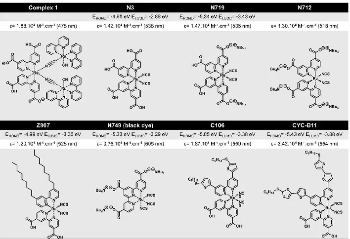
Figure I-15: Molecular structure of Ru-dyes with their related HOMO-LUMO levels and their extinction coefficient.
In their first DSSC[40], Grätzel and O’Regan investigated Ruthenium (Ru) complex dye of the
general structure [RuL2(μ-(CN)Ru(CN)L′2)2] where the L ligand is
2,2′-bipyridine-4,4′-dicarboxylic acid and the L′ ligand is 2,2′-bipyridine known as “complex 1” previously synthesized by Nazeeruddin (pioneer of Ru complex dyes in DSSCs)[85]. This trinuclear Ru complex has the advantage of absorbing a very wide range in the visible with a molar extinction coefficient of 1.88 x 10⁴ mol-1.L.cm-1 at 478 nm assigned to the electronic
transition stemming from the metal to the L ligand, the well-known MLCT transition. The L ligand is structurally designed for grafting onto the oxide layer especially through the carboxylic functions. By cleaving the two cyano (CN) bridges in thiocyanato (SCN) derivatives, the trinuclear structure has been simplified by the design of novel mononuclear Ru complex dye, cis-RuL2(NCS)2, coded as N3 dye[86]. The introduction of thiocyanate ligands extended the
absorption to more than 800 nm with higher ε (Figure I-15). However the open circuit potential (Voc) of the cell using this dye is similar to the complex 1 dye having the same anchoring group.
24 Indeed when, the carboxylic acid is substituted by the carboxylic salt tetra-n-butylammonium TBA+, the acidity is decreased affecting the energy level of the semiconductor conduction band
to more positive potential so the Voc is increased. Such is the case with N719 and N712
dyes[87,88].
Within this vision and in order to extent the spectral response into the NIR region, the switch from the two bipyridyl ligands to a fully deprotonated terpyridyl derivative and three thiocyanato ligands triggered the LUMO level of the“black dye” or N749to more positive potential leading to the MLCT shift toward longer wavelengths and its absorption is extended to NIR region up to 920 nm[89]. For all these dyes the light harvesting capacity is large following the IPCE (the relation is given in the next section) of more than 80 % in particular for N3 and N749. However regarding their long-term stability, hydrophobic chains as electron donors are introduced in the molecular structure to prevent the dyes desorption of the anchoring group caused by water. The most familiar is Z907 dye[90–93] for its durability and thermal stability showing high photovoltaic performances. This 4,4′-Substituted 2,2′-Bipyridyl ancillary ligands based dye has led to a set of novel dyes containing either aliphatic groups such as K51[94], K68[95], A597[96] or aromatic groups such as K77-7[97], IJ-1[98], JJ-12[99] or both such as HRS-1[100], TG6[101], C106[102] (Annex I-1). Interestingly, using these dyes in DSSCs, the recombination has reduced considerably between the oxide semiconductor and the hole conducting material coming from the addition of hydrophobic side chains which minimize their contact. In the work conducted by Kroeze et al. the longest hydrocarbon chain length displays a fast charge separation and slow recombination in DSSCs[103].
The last category of dyes combining aliphatic and aromatic groups has the best performances in DSSCs notably the CYC-B11 dye[104] (molecular structure quasi-similar to C106) reported by
Chen et al. incorporating an electron-rich hexylthio-terminal chain showing the best ε value (2.42 x 10⁴ mol-1.L.cm-1) when compared to all Ru based dyes with a top efficiency of 11.5 % (Figure I-16).
25 Figure I-16: (a) Photocurrent density−voltage characteristic curves of championship Ru-Dye, CYC-B11 and its molecular
structure. (b) Incident photon-to-current conversion efficiency spectrum of CYC-B11.
All Ru based dyes have been well reviewed by Nazeeruddin[105]. Ru is actually targeted as d6 transition metal for photosensitizers due to its octahedral symmetry, and its interesting redox properties triggered by light inducing the MLCT. However, this noble Ru metal is expensive and is in limited supply and even toxic. Therefore other d6 metal photosensitizers have also been developed such as osmium (Os)[106], rhenium (Re)[107] and iron (Fe)[108] resulting in a light absorption extension to higher wavelengths, in an interesting interfacial electron transfer behavior and in a high quantum yield respectively[109],[110]. Other organometallic complexes have been investigated based on d8 metal such as platinum (Pt)[111], iridium (Ir)[112] and copper (Cu)[113]. Environmentally friendly photosensitizers extracted from flowers, vegetables, fruits and leaves have also been collected as alternative to Ru-complexes[114]. They are either in the form of
metal-complex or metal-free dyes. Metal-complex chlorophyll based dyes are the most efficient natural pigments (η~4.6 %)[115] followed by anthocyanin dyes (η~2.9 %)[116]. Even though their
preparation is easier and cost effective, they photodegraded because of the presence of free radical ions arising from excited electron from photocatalytic activity of TiO2 and moisture[117].
Therefore, DSSCs sensitized with organometallic dyes are unstable leading to low photovoltaic performances as compared to synthetic metal-free organic dyes.
26
I.2.b .(ii ) Metal-free dyes
Figure I-17: Molecular structure of some organic dyes used in DSSCs.
Organic photosensitizers are the most attractive candidates as alternatives to Ru dyes owing to their high molecular extinction coefficient, their low production cost, their easy and versatile synthesis and their wide variety for the molecular structure design as well as their pleasing range of colors across the visible spectrum, from deep red to violet. In 1998, Arakawa and coworkers first reported DSSC based on organic dye, eosin Y (Figure I-17), leading to efficiency of up to 1.3 %[118]. Later and following the work done by Kamat using merocyanine dye for electrochemical cell[119], the same group has studied a series of this dye, by modifying either the anchoring group, usually carboxyl group, or the alkyl chain type[120]. Obviously as mentioned earlier, the long hydrophobic chain based dye Mb(18)-N gave the highest efficiency (4.2 %). Since then they investigated different pure organic dyes such as mercurochrome[121], and coumarin derivative[122]. Meanwhile, Wang et al. developed a DSSC based on hemicyanine dye with an overall yield of 2.1 % showing the highest short circuit photocurrent density (Jsc= 15 mA.cm-2) and the highest IPCE of nearly 100 %[123]. This hemicyanine photo-sensitizer
27 shows particularly a π-conjugated bridge between the methyl azolium propylsulfonate as electron acceptor (A) and the 4-[bis(methyl)-amino]benzyl as electron donor (BTS dye).
Figure I-18: Schematic representation of a donor-π-conjugated bridge-acceptor dye
The introduction of the π-conjugated bridge into the D-π-A framework (Figure I-18) enhances the intramolecular charge separation simultaneously toward the donor and the acceptor: this is called the “push-pull” effect[124]. Moreover it shifts the dye’s HOMO and LUMO frontiers energy levels
affecting its intramolecular charge transfer (ICT) from the donor part to the electron acceptor part, and hence its absorption ability (in wavelength and/or in molecular extinction coefficient). For these reasons, the research work was directed toward the conception of novel fragments constituting the dye structure (donor, π-linker, and acceptor units) to optimize the overall yield[125].
Electron donor moiety (D) :
28 Typically the donor part of the dye is composed of an electron rich moiety where the HOMO energy level is lying on. Many efficient donor substituents were employed including indoline[126-128], coumarin[129–131], fluorene[132], phenothiazine[133–135], carbazole[41,136,137] and
triphenylamine (TPA)[138,139].
TPA, through its starburst-like structure containing a nitrogen atom center bonded by three neighboring aromatic rings (Figure I-19), is the most popularly used donor unit in view of its strong electron donor ability and hole mobility and its non-planar configuration preventing intermolecular aggregation[140]. TPA was first incorporated into organic light-emitting diodes (OLEDs) and into organic field-effect transistors (OFETs)[141] before Yanagida and coworkers initiated it as donor based dye (ε= 2.5 x 10⁴ mol-1.L.cm-1) into DSSCs giving an efficiency of
5.3 %[142]. The reported IPCE is up to 80 % but is further improved for a novel type of TPA (ε= 3.9 x 10⁴ mol-1.L.cm-1) in presence of fluorene (IPCE= 91 %) which gave an efficiency of
nearly 8.1 %[143] with high Jsc and Voc. Few years later, Feldt et al. highlighted the importance of
alkyl bulky chain, here butoxy chain for D35 (Figure I-17), on TPA core used for reducing the charge recombination between the hole conducting material and the oxide semiconductor[144]. Considering this, Yella et al. combined both fluorene moiety and butoxyl chain to TPA core giving rise to an efficiency of 10.3 % under full sun[145] : the top efficiency for TPA based dyes (Figure I-20). In the following report, the study will be restricted to TPA donor based dyes.
Figure I-20: (a) Photocurrent density−voltage characteristic curves of the TPA championship dye (JF419) in liquid DSSC device with 0.25 M (left) and 1 M (right) 4-tert-butylpyridine (TBP) at different light intensity (b) JF419 molecular
29 Electron acceptor as anchoring group (A):
The electron acceptor part is employed as electron withdrawing unit and as anchoring group to allow an optimal electron injection into the oxide semiconductor. Therefore the LUMO is spatially located in the anchoring group. A recent review, Zhang and Cole present anchoring groups in DSSCs[146] and they reported that cyanoacrylic group is more suitable for organic dyes than pyridine, perylene dicarboxylic acid anhydride, tetracyanate, 2-hydroxybenzonitrile, etc. owing to its two strong negative mesomeric effects. However carboxylic group is exclusively bonded to the oxide semiconductor (TiO2) surface through mainly bidentate bridging[147]
involving covalent bond (Figure I-21) between metal of the semiconductor and the dye in solution (chemisorption). So far, most of D-π-A dyes hold the cyanoacrylic anchor[148–152].
Figure I-21: Molecular structures of the different acceptor group.
Conjugated bridge (π):
Researchers attach great importance to the structural engineering of the π-conjugated bridge which considerably shifts the wavelength and the molecular extinction coefficient. Yanagida and coworkers were the first to promote the TPA and cyanoacrylic acid as electron donor and acceptor respectively[142], using a conjugated oligoene spacer. They emphasize that extension of the conjugated chain impact the dyes spectral response due to the expansion of π-electron systems conjugated with a phenyl ring leading to higher efficiency.
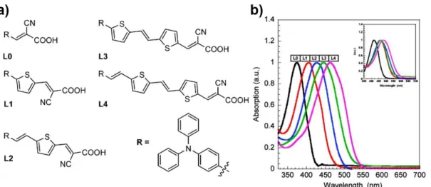
30 Figure I-22: (a) Molecular structure of series of dyes L0, L1, L2, L3, L4 and their (b) their normalized absorption spectra
in ACN from ref. [124].
Hagberg et al. reported a D-π-A dye with the thiophene as π-conjugated bridge, following the work conducted by Hara et al.[153], yielding an efficiency of 5.1 %[154]. This dye coded as D5 and also as L2 (Figure I-22a) has been later compared to a series of chromophore by extending π-bridge with more than one thiophene unit[124]. As illustrated in Figure I-22b the absorption is
coherently red-shifted with the conjugation increase, but the charge recombination is also increased due to the binding and orientation problems of the dye.
In addition to oligoene and thiophene or polythiophene[155], other π-conjugated bridge have been
developed such as benzothiadiazole[156,157], benzotriazole[158,159], and
cyclopentadithiophene[145,160,161] (Figure I-23). The latter has the benefit to hold hydrophobic alkyl chains preventing the hole conducting material to reach the oxide semiconductor.
Figure I-23: Molecular structures of the first D-π-A dye developed by Yanagida et al. and of the different π-conjugated bridge group.

![Figure I-25: Record efficiency obtained by Tian et al. [184] in (a) s-DSSC using S5 as dye and (b) Spiro-OMeTAD as HTM](https://thumb-eu.123doks.com/thumbv2/123doknet/2332107.31944/43.918.161.776.540.770/figure-record-efficiency-obtained-tian-dssc-spiro-ometad.webp)