Carbon Nano-Relays for Low Power Switching
by
Kaveh Mehdi Milaninia
B.S., University of California at Berkeley (2003)
Submitted to the Department of Materials Science and Engineering
in partial fulfillment of the requirements for the degree of
Doctor of Philosophy in Materials Science and Engineering
at the
MASSACHUSETTS INSTITUTE OF TECHNOLOGY
September 2009
@ Massachusetts Institute of Technology 2009. All rights reserved.
ARCHIVES
A uthor...
...
...
Department of Materials Science and Engineering
August 11, 2009
Certified by...
Certified by.
Associate
Accepted by...
Marc A. Baldo
Associate Professor of Electrical Engineering
Thesis Spervisor
Francesco Stellacci
Professor of Materials Science and Engineering
,I
Tlis
Supf~cisor
Chri...stine rtiz
Christine rtiz
Chair, Departmental Committee on Graduate Students
ACHUSETS NSTWrmTE
OF TECHNOLOGY
SEP 0
9
2009
Carbon Nano-Relays for Low Power Switching
by
Kaveh Mehdi Milaninia
Submitted to the Department of Materials Science and Engineering on August 11, 2009, in partial fulfillment of the
requirements for the degree of
Doctor of Philosophy in Materials Science and Engineering
Abstract
In this thesis two unique carbon based nanoelectromechanical switches or carbon nano-relays are demonstrated as a toolkit for investigating NEMs based low power switching. The first is a vertical carbon nano-relay, consisting of a vertically aligned carbon nanotube/fiber (CN) between two contacts and operated by pull-off, and the second, a double graphene switch, consisting of two electromechanically actuated stacked layers of polycrystalline graphene.
Vertical carbon nano-relays were initially prototyped by inserting a CN between two contacts through the use of a nanopositioner. The prototype demonstrated pull-off operation and multiple switching. To our knowledge this is the only example to date of a multiple-use NEMs switch that operates with pull-off. Next a wafer inte-grated device was fabricated. Although pull-in was demonstrated in these inteinte-grated devices, pull-off was not possible primarily due to limitations in CN growth, which were also investigated.
In the work on a double graphene switch we demonstrated an electromechanical switch comprising two polycrystalline graphene films, each deposited using ambient pressure chemical vapor deposition (CVD). The top film is pulled into electrical con-tact with the bottom film by application of approximately 5V between the layers. Contact is broken by mechanical restoring forces after bias is removed. The de-vice switches several times before tearing. Demonstration of multiple switching at low voltage confirms that graphene is an attractive material for electromechanical switches.
Thesis Supervisor: Marc A. Baldo
Title: Associate Professor of Electrical Engineering Thesis Supervisor: Francesco Stellacci
Acknowledgments
As I near the end of my time as a Ph.D. student, I am happy to finally have the opportunity to thank and acknowledge all of those that I have made my Ph.D. possible be it by valuable discussions, assistance in the lab, or even with a much needed pat on the back.
First off I would like to thank Professor Marc Baldo for being my advisor and for his financial support over the years, as well as Professor Caroline Ross, Professor Francesco Stellacci, and Professor Tayo Akinwande for their time as members of my thesis committee. In particular, I'd like to thank Professor Akinwande for his invaluable discussions and feedback on much of my work, and especially his constant encouragement and positive reinforcement for which I'm truly thankful. In the end he managed to convince even a diehard Cal fan such as myself, that Stanford isn't that bad after all.
For their contributions to my work on vertical carbon nano-relays, I owe a great debt of gratitude to my collaborators Courtney Schmitt, who not only worked side-by-side me on the project for two years but was essentially in keeping me focused and organized throughout the entire process, and Luis F. Velsquez-Garca, who, despite having one of the busiest schedules I have see, still made time to help work on and discuss key aspects of the project. And of course, none of the work would have been possible without Bob Bicchieri and his constant maintenance of CCNT tool which was critical to my research on vertical carbon nano-relays.
For his assistance on my work on a double graphene switch, Alfonso Reina-Cecco deserves a great deal of credit for not only providing me with the essential CVD graphene that made the switch possible, but for also teaching me everything necessary to process and handle the material as well. This work would also not have been made possible without Professor Jing Kong's willingness to allow me virtually free access to her lab, as she has done on many occasions throughout my time at MIT. In addition, Hootan Farhat, Mario Hofmann, Kyeong-Jae Lee, Daniel Nezich, Hyesung Park, Joel K. Wang and Michele Zaffalon all provided valuable assistance in getting the device
fabricated.
Overall, my work at MIT was made possible through many of the valuable mem-bers of the MIT community many of whom I consider good friends. Much of my work was done at shared facilities at MIT, such as NSL. These labs not only granted me access to equipment to complete mly work, but also to a commnnunity of highly ex-perienced individuals such as Professor Hank Smith, Professor Karl Berggren, Mark
Mondol and Jim Daley, all whom were more than willing to sit down with me and allow nme access to their vast knowedge. Jim, especially, who amongst a numerous number other things always expedited whatever "emergency" work I had that ur-gently needed to be done. There were also members of the general MIT community such as Tim Savas, Riccardo Signorelli, and Stevie Steiner to name a few, that were always there to discuss and provide their input on new and old ideas. Despite what MIT may have lacked as far as equipment and research capabilities, the community here at MIT is truly unique and has been my and is its greatest assets.
I am also grateful for all the time I have spent and knowledge I have exchanged my past and the current group members of the Soft Semiconductor Group: Milhai Bora, Kemal Celebi, Mike Currie, Ying Gao, Shlomy Goffri, Tim Heidel, Priya Jadhav, Jiye Lee, Benjie Limketkai, Evan Moran, Carlijn Mulder, Phil Reusswig, Kelley Rivoire, Carmel Rotschild, Michael Segal, Raja Singh, Luke Theogarajan, and Nan Yang. In particular my friendships with Mihai, Benjie, and Luke are what I have and will value more than anything else from my time at MIT.
I am thankful to all my friends both at and outside of MIT that have helped cheer me up during the bad times and celebrate with me during the good times. Even though there are many of you out there, I'd like to just give special thanks to Katchi,
Sanaz, Lady, Yoda, Jamal, and Rouzy.
Finally, I would like to thank my family, in particular my parents Ali and Iman, who not only brought me into this world but have and continue to support my time throughout it in every way they (can, and, of course, my sister Kimya, who among
Contents
1 Motivation 1.1 Background... 1.1.1 MOSFET 1.1.2 Dynamic Powe 1.1.2.1 Powe 1.1.2.2 Switc r. r . . . . r-Delay I hing spe 1.1.3 Static Power . 1.1.3.1 Gate Leakage 1.1.3.2 Subthreshold 1.2 Fundamental Limits of Power 1.3 Case for NEMs . ...1.3.1 General Theory . ...
1.3.2 Potential Solution . . . 1.3.3 Ion Channels . . . . . 1.4 Our approach to address these 1.4.1 Carbon Nanotubes . . 1.4.2 Device ... 1.5 Thesis Overview ... 'roduct .
ed . ....
Leakage Dissipation problems2 Theory and Design
2.1 NEMs Relay: Continuum Model . 2.1.1 Van der Waals ...
2.1.2 Electrostatic ... 23 23 26 26 27 28 29 29 30 32 35 35 36 36 37 39 39 40 . . . . . . . . . . . .
2.1.3 Elastic ... ... 46
2.1.4 Pull-In Scaling ... ... 48
2.2 Previous Approaches ... ... .... 48
2.2.1 Horizontal 3-Terminal CNT Relay . ... 49
2.2.2 Vertical 3-Terminal CNT Relay ... 50
2.2.3 Vertical 3-Terminal CNT Relay with Pull-Off . ... . . .52
2.3 Stiction ... ... .. 55
2.4 Challenges and Design Requirements ... 56
3 Prototyping 59 3.1 Proof of Concept ... ... .. 59
3.1.1 Testing Setup ... ... . 59
3.1.2 Tube Attachment ... ... 60
3.1.2.1 van der Waals attachment . ... 60
3.1.2.2 Electron Beam Induced Deposition ... .. 61
3.1.2.3 Dielectrophoretic attachment . ... 62
3.1.3 Experimental Procedure ... ... 63
3.1.3.1 Two Terminal Measurements . ... 63
3.1.3.2 Three Terminal Measurements ... .... 64
3.1.4 Results ... 65
3.1.4.1 Two Terminal Measurements ... ... . 65
3.1.4.2 Three Terminal Measurements . ... . . 65
3.2 Initial design ... ... 69
3.3 Fabrication . .... ... ... 69
3.4 Issues . . . ... ... .. ... . 70
4 Integration 75 4.1 Need for integration ... ... .. 75
4.2 Fabrication ... ... .. 75
4.2.1 CN Growth ... ... ... ... 79
4.2.1.1 CN PECVD Primer . ... 80 8
4.2.1.2 Catalyst Selection . ... ... . 81
4.2.1.3 Growth Limitation . . . ... 84
4.2.2 Oxide Deposition ... ... 92
4.2.3 a-Si Deposition ... ... 98
4.2.4 Self-aligned Spin Planarization . ... 99
4.2.5 Contact Etch ... ... 100 4.2.6 Release. ... ... .. 101 4.2.7 Results. ... .. 102 4.3 Measurements ... ... .. 102 4.3.1 Voltage vs Gap . ... . 102 4.3.2 Best Case ... ... 106
5 Double Graphene Switch 109 5.1 Introduction ... ... ... ... 109
5.2 Fabrication . ... ... .. 110
5.3 Results and Discussion ... ... 115
6 Conclusion 119 7 Future Work 121 7.1 Vertical Carbon Nano-Relay . ... ... 121
7.1.1 Fabrication . ... ... 121
7.1.1.1 Carbon Nanotube/Fibre . ... 121
7.1.1.2 Gap Size ... ... 122
7.1.2 Architecture for CMOS . ... ... .. 122
7.2 Double Graphene Switch ... ... 122
7.2.1 Reliability ... ... . 122
7.2.2 Noise ... ... .. 123
7.3 Nanomechanics and Surface Forces ... 124
7.4 Subthreshold and Multiple Charges . ... 125 9
8 Appendix A: Circuit Integration 127 8.1 Circuit Applications ... . ... 127 8.1.1 Reconfigurable Interconnects ... 128 8.1.2 Power-Gating ... . . . . . 128 8.1.3 Nonvolatile Memory ... ... . 129 8.2 Packaging .... . ... ... ... 129 9 Appendix B: Figures 131 10 Appendix C: Tables 135 11 Appendix D: Fabrication 139 11.1 Fabrication of an Integrated Vertically Oriented Carbon Nanorelay 139 11.1.1 Catalyst Diffusion Barrier ... . 139
11.1.2 Photoalignmnent Mask Layer ... 140
11.1.3 Carbon nanotube/fibers ... .. 141
11.1.3.1 Catalyst Patterning ... 141
11.1.3.2 Growth . ... ... 142
11.1.4 Contacts . . . ... . ... . ... 142
11.1.4.1 Deposit Materials ... . 142
11.1.4.2 Create Etch Mask ... ... . . 143
11.1.5 Release . ... . . .. . . .. ... . 144
List of Figures
1-1 Power trend versus time. Source 2003 and 2005 International Technol-ogy Roadmap for Semiconductors update. . ... 24 1-2 Clock rates versus time. Highlights the recent trend in reducing clock
rate for dynamic power reduction. ... . . . 25 1-3 A CMOS inverter consisting of a PMOS (top) and NMOS inverter
(bottom) in series. Assuming that two CMOS inverters are cascaded the second CMOS inverter is modeled by a capacitor. . ... 25 1-4 (a) A schematic of an n-type MOSFET (NMOS). (b) Electrostatic
coupling in FET may be modeled by two capacitors. ... 27 1-5 a) Gate leakage arising from current flow between the gate to the drain
when the MOSFET is turned "on" and b) Subthreshold leakage arising from current flow between the source and the drain when the MOSFET is turned "off" ... ... . 29 1-6 An NMOS and the corresponding conduction band energy diagram. 31 1-7 Plot of the source-drain current as a function of gate-source bias. . 32 1-8 Plot of the source-drain current as a function of gate-source bias for
various Vth. . ... . .. . . 33 1-9 Plot of the source-drain current as a function of gate-source bias for
various S. ... . 33 1-10 Comparison of a) conventional single molecule FET to that of a b)
mechanical single molecule FET ... ... .. . . 34 1-11 Mechanical Relay ... . ... 37 1-12 Voltage dependent K+ channel ... .. . . 38
1-13 Data for a voltage gated ion channel. Hodgkin and Huxley, J.. Physiol.
116, 449 (1952a) .. . . .... .... . . 38
1-14 Structure of a carbon nanotube from a sheet of graphene ... . 40
1-15 Proposed device for studying nanoelectromechanical systems ... 41
1-16 Operation of a Vertically Oriented Carbon Nanorelay ... . 41
2-1 Forces involved in a carbon nano-relay. Schematic of: a) an vertical carbon nano-relay showing relevent dimensions. b) an activated ver-tical carbon nanorelay showing relevent forces. c) a horizontal beam relay showing relevant dimensions and d) an activated horizontal beam relay showing relevent forces ... .. . 44
2-2 Horizontal 3-Terminal CNT Rela.y ... .. 50
2-3 Data for Horizontal 3-Terminal CNT Relay in a) non-contact mode allowing for at least two iterations and b) contact mode where the device suffers from stiction to the contacts . ... 51
2-4 Example of several different devices built by the Cambridge group. Shown Top: As fabricated and Bottom: Under activation . ... 52
2-5 Top Left: Scanning electron micrograph of an as fabricated three-carbon nanotube switch. Top Right: SEM micrograph of the same device after the removal of an applied bias. The scale bar corresponds to 1 pmu . Bottom: Current versus voltage characterstics. ... . 53
2-6 Two two-carbon nanotube switches that were tested. a) Device made with high-aspect ratio tubes Top Left: Scanning electron micrograph of an as fabricated two-carbon nanotube switch. Top Right: SEM mi-crograph of the same device after the removal of an applied bias. The scale bar corresponds to 1 p Bottom: Current versus voltage charac-teristics. b) Device made with low-aspect ratio tubes . ... 54 2-7 a) Schematic of a vertically oriented carbon nanotube relay created by
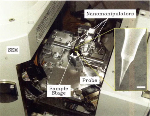
3-1 Photograph of the Zyvex S100 Nanomanipulator installed on a JEOL JSM-6060 SEM. The inset is a scanning electron micrograph of an etch tungsten wire probe for making electrical contact. The scale bar
corresponds to 100 pm .l... ... 60 3-2 Scanning electron micrograph of CN attached to a tungsten probe using
van der Waals attachment technique. The scale bar corresponds to 20 p C l . . . .... . . . . . . . .. . 6 1 3-3 Scanning electron micrograph of a) cross-section of a forest of CNs
grown via thermal CVD. The scale bar corresponds to 50 /pm. b) top view of a cleaved section showing isolated CNs. The scale bar corresponds to 5 pm. ... ... ... 62 3-4 Scanning electron micrograph of a CN attached to a tungsten tip. The
dotted circle represents the area which was magnified under the micro-scope to deposit the carbonaceous material. The scale bar corresponds to 2 pim . . . .... . . . . . .. 63 3-5 Schematic of the DEP setup (a) before and (b) after being drawn from
a CNT solution. . ... ... .. 63 3-6 Scanning electron micrograph of a CNT bundle attached probe by
DEP. The scale bar corresponds to 10 pmn . ... 64 3-7 The setup of a two terminal measurement for pull-in. (a) The CN
attached probe is grounded, and a voltage sweep is applied to the other probe. (b) As a result, the tube is pulled in to one side .... 64 3-8 The setup of a three ternninal measurement for pull-in and pull-off. 66 3-9 Scanning electron micrograph of a CN bundle a) before and b) after
pull-in. The scale bar corresponds to 20 yim. . ... . 67 3-10 I-V measurement for a two terminal measurement. Corresponds to the
scanning electron micrographs in Figure 3-9. . ... 67 3-11 Scanning electron micrograph of a) CN attached probe. b) Same probe
used in a three terminal measurement after step 1, c) step 2 and d) step 3. The scale bar corresponds to a) 20 pm and b,c,d) 10 pm. . . 68
3-12 I-V measurement for a three terminal measurement. Corresponds to the scanning electron micrographs in Figure 3-11. . ... . . 69
3-13 Initial fabrication route for integration and prototyping. Schematic of various stages of fabrication: a) substrate with thermal oxide, b) pho-tolithographically patterned gold contacts, c) coating of the electron beam resist, d) exposed and developed trench pattern in resist, e) resist masked etching of the metal contact, f) resist masked etching of the oxide, g) resist masked etching of the silicon, h) deposition and lift-off of the metal catalyst, i) growth of the tube, and
j)
the final device. 713-14 Micrographs of initial fabrication efforts. a) Photomnicrograph of a Au on Cr beam schematically shown in Figure 3-13b. b) Scanning electron micrograph of the gap defined via a PMMA mask after the oxide etch schematically shown in Figure 3-13f. The scale bars correspond to a) 100 upm and b) 1 pm. ... ... 72
3-15 Cross section scanning electron micrograph of the initial fabrication efforts after the liftoff of the catalyst schematically shown in Figure 3-13i. The inset is a high contrast tilted scanning electron micrograph of the channel showing the 100nm Ni wide catalyst line . The scale bars correspond to 2 pm. ... ... ... . . 72
3-16 Scanning electron micrographs of a CN attached bundle via DEP, a) before and b) after testing. The scale bars correspond to 2 pm... 74
3-17 The equivalent circuit of the NEM. On contact the switch closes and the capacitor discharges. The discharge current can destroy the tube
4-1 Fabrication carbon nanotube based gated field emitter. The scanning electron micrographs show various stages of the fabrication: a) the growth of carbon nanotube, b) the top of the emitter poking out of the resist after the use of a self-aligned photoresist planarization technique,
c) the same device after an a-Si etch and removal of the photoresist, and d) the final device. ... ... 77
4-2 Schematic of fabrication process for a fully wafer integrated vertical carbon nano-relay: a) Bare silicon wafer, b) sputter deposited TiN layer, c) lift-off patterned catalyst sites, d) CN grown, e) PECVD ox-ide deposition, f) PECVD a-Si deposition, g) spun resist, h) patterned resist, i) etched resist, j) etched a-Si, k) ashed resist, and 1) final re-leased structure. ... ... .. 78
4-3 Schematic of PECVD reactor and synthesis of vertically oriented car-bon nanotubes. The PECVD reactor for nanotube growth is similar to a standard PECVD reactor in that it consists of a vacuum chamber in which we have two electrically isolated electrodes. A growth gas in then introduced into the chamber, a plasma is sparked, and material is then deposited in the system. The primary difference is the the bottom electrode, on which the substrate sits, is in close proximity to a high temperature heater. High temperatures are necessary to "ac-tivate" the catalyst for nanotube growth. In addition, as opposed to a conventional PECVD where the material is deposited everywhere, growth only occurs underneath the catayst ... 81
4-4 Schematic drawing of the growth cycle of carbon nanotubes derived from patterned catalyst. Initially the catalyst and substrate are pre-treated, typically involving heating of the substrate under some sort of inert or reducing environment. Growth begins when carbon is intro-duced, and diffused into the catalyst. The carbon nanotubes can then grow by either having the carbon precipitate out from the top of the catalyst resulting in a base growth or from the bottom of the catalyst resulting in a tip growth. . ... ... . . . 82 4-5 Scanning electron micrographs of a nanotube forest showing evidence
of a tip based growth mechanism. a) Shows the image of the forest as grown, the inset is of the edge of the sample and shows ain alternative contrast the bright and dark spots, respectively show the location of the nickel catalyst. The scale bar corresponds with 1pm b) Shows the same image after the sample was placed in nickel etchant. The arrow points to the location where the catalyst was removed. The scale bar corresponds to 200nm. Samples were grown from a 10 mn Ni film on a 50 TiN on silicon substrate. ... .. 83 4-6 Scanning electron micrographs of carbon nanotube forests grown from
a) cobalt, b) iron, and c) nickel. All three samples were grown under the same conditions at the same time ... .... ... .. 85 4-7 Scanning electron miicrographs of a line of carbon nanotubes. Line
shows how the height of the nanotubes decreases with decreasing cat-alyst volume. Catcat-alyst sizes decrease by 50ran every 11pmn. The scale bar corresponds to 10 pm. ... ... ... 86 4-8 Scanning electron micrographs of a pre-patterned catalysts of varying
size and their corresponding carbon nanotubes. Non-labeled scale bars corresponds to 1 pm. . ... ... 87 4-9 Plot of the catalyst size versus bottom carbon nanotube diameter. All
4-10 Plot of the catalyst size versus carbon nanotube height. All measure-ments were taken from the same sample during a single growth. . . . 89 4-11 a) Schematic of nickel sputter off. b) Scanning electron micrograph of
nickel catalyst at the tips of the nanotubes that are being sputtered off. The scale bar corresponds to 200 nmn. . ... . 90 4-12 Plot of the catalyst thickness versus carbon nanotube height. ... 91 4-13 Schematic of the fabrication of the device after tube growth a) starting
with a line of CNs, grown with a pitch, p, b) growth of a PECVD oxide with thickness, t,,o and c) the deposition of the contacts and final
processing. ... ... . ... .. 93
4-14 Schematic of the ideal growth of a conformal oxide with showing a) the original line of CNs, b) the undergrowth of oxide, b) (upper) the minimum thickness of oxide required optimal growth and (lower) the optimal growth of oxide with given factor of safety, and d) an undesired overgrowth of oxide. ... ... 94 4-15 Schematic of the fabrication of the device in which the oxide between
tubes did not coalesce leading to a short between the two electrodes. 95 4-16 Scanning electron micrograph of a device with an undergrowth of oxide.
The scale bar corresponds to 20011n. ... 95 4-17 Schematic showing a) two different growth rates the first being the
faster, uniform rate of oxide growth, rgox,gap and the second being the slower rate of oxide growth, rgox,fill, between the tubes and b)the resulting growth of this asymmetric growth rate . ... 96 4-18 Schematic of the ideal growth of a conformal oxide with showing a)
the original line of CNs, b) the undergrowth of oxide, b) (upper) the minimum thickness of oxide required optimal growth and (lower) the optimal growth of oxide with given factor of safety, and d) an undesired overgrowth of oxide. ... ... 97
4-19 Schematic of the two oxide growth models resulting in asymmetric growth and voids, a) the conventional "mushroom" type growth and b) the proposed charge induced asymmetric growth. ... 98 4-20 Tilted scanning electron micrograph of a row of nanotubes after the
oxide and a-Si deposition. The scale bar corresponds to 10 pm... . 99 4-21 Schematic of the self-aligned contacts by spin planarization used in this
work ... .... ... 100
4-22 Tilted scanning electron micrograph of a device after the reduction in the height of the resist by etching. The scale bar corresponds to 2 pm 101 4-23 Tilted scanning electron micrograph of a device released using vapor
HF. The scale bar corresponds to 1 pm . ... .. 102 4-24 Scanning electron micrograph of a fully fabricated device from the a)
top and b) tilt view. The scale bars correspond to 2 pm.in. ... 103 4-25 Setup for pull-in voltage versus gap measurements using 10 pm
nan-otubes. The scale bar corresponds to 1 pm . ... 104 4-26 Pull-in voltage versus gap size for a single tube. Experimental
mea-surenments plotted alongside model . ... 105 4-27 I-V plot of a fully integrated device showing pull-in as well as stiction
during the second run. ... ... 107
5-1 Schematic diagram of a double CVD graphene switch shown from a) a cross-sectional view and b) a top down view . ... . . 111 5-2 Operation of a double layer graphene switch starting from the a) "off",
b) then the beginning of the pull-in stage when the applied bias V is less than the pull-in voltage and also showing the forces acting on the top beam, c) the final "on" state when V is greater than or equal to the pull-in voltage, and finally d) the restored "off" state upon removal of the bias ... . ... .. 111
5-3 Schematics of the fabrication process for a double CVD graphene switch. The following steps are shown: a) doped silicon substrate, b) bottom layer of graphene on the silicon substrate, c) PECVD deposited SiO2, d) patterned contacts, e) a transfered top layer of graphene, f) the PMMA resist mask, g) patterned PMMA beam, h) pattern transfer of the PMMA beam to the graphene, i) removal of the PMMA, and j) etch and release of the device. ... ... 112 5-4 Photomicrographs of a) a typical CVD grown graphene film showing
domains of .1-2 and multilayer graphene growth, b) a double CVD graphene device after the second or top layer of graphene has been transfered with various areas containing no graphene, just the top graphene and both the top and bottom graphene layers, c) (left) a patterned PMMA beam on the top graphene and (right) the transfer of that beam to the bottom graphene after an oxygen plasma etch and finally d) an electron micrograph of a completed device. ... . 114 5-5 I-V measurements between the top and test electrodes of similar
de-vices before and after the final step in the fabrication process, the HF etching of the oxide . . . . ... . ... 114 5-6 Current-Voltage characteristics between the top and bottom contacts
for a w=3ptm, L=60pm, and g=500nm device showing multiple events of switching. i) First scan, ii) Third scan (from 0 to 5V only), and iii)the fourth and final scan. . ... . .. 116 5-7 Electrical and physical evidence of mechanical failure in large area
CVD graphene switches. a) I-V data of the graphene beam measured through the Top and Test contacts before switching measurements and after switching measurements. b)Scanning electron micrograph of de-vice after testing. Inset is a magnified image of tear in graphene beam. 117
7-1 For complementary logic a fourth terminal is required to pull the tube
7-2 Example data extracted from works by Lee et al.[42] Data is presented here to highlight the noise observed in carbon nano-based relays. a)
I - VI data for device with multiple switching events, and b) I - ,g
data for device which operated for a single switching event. ... . 124 7-3 Schematic of a graphene film being mechanically tested in a double
graphene switch, prior to electromechanical testing. ... . 125 8-1 Circuit diagram of a ring oscillator implementing a nano-relay as a
reconfigurable interconnect . ... .... . 128 8-2 Circuit diagram of a power gate. ... .. 129 8-3 Circuit diagram of a nano-relay based nonvoatile memory cell. ... 130 8-4 A carbon nanorelay delay epoxied in the cavity of a ceramic side braze
and wirebonded ... ... . . . 130
9-1 Measurement of CVD graphene thickness. a) AFM micrographs of a CVD graphene sheet on SiO2 showing regions of varying thickness
graphene and bare SiO2, b) step height measurements by AFM of the
graphene thickness taken at regions indicated by the lines and arrows. The scale bar corresponds to 1 npm.[56] . ... 132 9-2 AFM micrographs of Cr/Au gold contacts a) before and b) after
List of Tables
4.1 Comparison of several catalysts based on the average nanotube height and tip diameter as well as distributions of both parameters. ... 84 4.2 Varying plasma anneal time while keeping nickel thickness constant.. 91 10.1 List of Procedure and Tools used in the ICL, TRL, and NSL
Chapter 1
Motivation
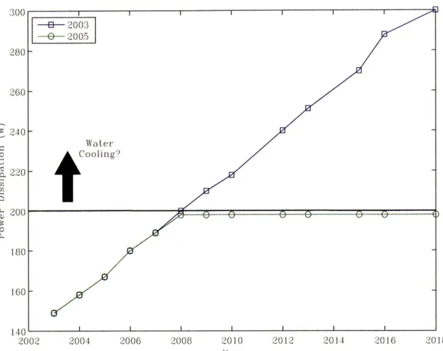
According to the latest edition of the International Technology Roadmap for Semi-conductors (ITRS), power consumption, and thus dissipation, are now the major problems facing the semiconductor industry. [1] In fact Figure 1-1 shows expected power trends from the ITRS roadmap for 2003 and 2005, indicating that after about 2005 power dissipation can no longer be increased due to limitations in system level cooling.
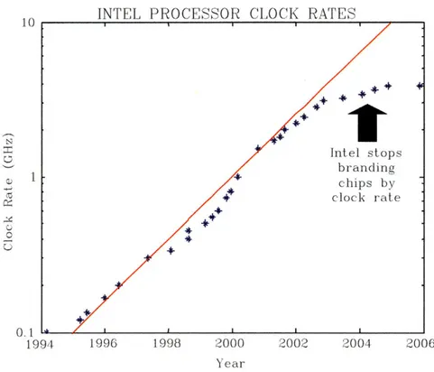
While a variety of techniques are available to reduce the dynamic power problem, such as device scaling, reductions in clock-speed (Figure 1-2), clock gating, dynamic voltage and frequency scaling, and better chip design used to circumvent non-essential computation, the static power dissipation, both with due to subthreshold and gate leakage have become extremely significant. Static power dissipation is still dominated by gate current leakage, but subthreshold current leakage is seen as the leading limi-tation since the development of high k-dielectrics as gate insulators have brought gate current leakage under control. [1]
1.1
Background
Most electronic devices today contain integrated circuits which use CMOS technology. (Figure 1-3) The power dissipated from these integrated circuits comes from two
300 280-260 . 240 Water a ~ Cooling? 200 % ,, .. , 180 160 140 2002 2004 2006 2008 2010 2012 2014 2016 2018 Year
Figure 1-1: Power trend versus time. Source 2003 and 2005 International Technology Roadmap for Semiconductors update.
0.1 l *
1994
INTEL PROCESSOR CLOCK RATES
1996 1998 2000 2002 2004 2006
Year
Figure 1-2: Clock rates versus time. Highlights the recent trend in reducing clock rate for dynamic power reduction.
VDD
VOUT
Figure 1-3: A CMOS inverter consisting of a PMOS (top) and NMOS inverter (bot-tom) in series. Assuming that two CMOS inverters are cascaded the second CMOS inverter is modeled by a capacitor.
Ptotal - Pdyn + Psat (1.1) The first of which is dynamic power, i.e. power that's dissipated anytime we turn one of these CMOS switching elements on and off, and the second of which is static power, i.e. the power that's dissipated when the device is not switching. In the past dynamnic power was the major contributor to the total power budget, and the solution to this problem was to scale down the device. Unfortunately, static or leakage power has increased exponentially as devices get smaller and smaller, and is now seen as the dominant contributor to power dissipation. Both sources of power dissipation will be discussed in the following sections.
1.1.1
MOSFET
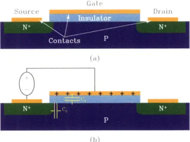
CMOS technology utilizes a pair of complementary imetal oxide semiconductor field effect transistors (MOSFETs), an n-type MOSFET (NMOS) and a p-type MOSFET (PMOS). A schematic of an NMOS is shown in Figure 1-4A. In an ideal MOSFET, current will only flow from the source to the drain upon electrostatic actuation of the channel via an applied gate-source bias or VGS that needs to be greater than a threshold voltage VT. For maximum gate control, it is important that the electrostatic coupling between the gate and the channel be greater than that between the source and the channel. These two electrostatic couplings can be modeled as two capacitors
CG, between the gate and the channel, and Cs, between the source and the channel,
Figure 1-4B. To achieve this level of gate control it is important that CGS >
CSD-1.1.2
Dynamic Power
It is important to know how a CMOS circuit functions and where the source of power dissipation in the dynamic regime arises. A model CMOS circuit is shown in Figure 1-3. In CMOS circuits, ideally, power is only dissipated during switching (dynamic power) and does not dissipate power in the steady state (static power). As an example, first consider the case when VIN is "low", i.e. VIN - 0, and and thus for the NMOS
; at e
((1)
Figure 1-4: (a) A schematic of an n-type MOSFET (NMOS). (b) Electrostatic cou-pling in FET may be modeled by two capacitors.
VGS < VT and for the PMOS VGs I-VDD > IVTI, where VT is the threshold voltage
required to turn the NMOS or PMOS on and thus the NMOS is off and the PMOS is on. Under this condition, the capacitor C is then charged to VDD and thus the output is considered "high". Considering the opposite case where the input is "high" i.e. VIN - VDD for reasons previous stated the NMOS is on and the PMOS is off,
the capacitor is then discharged through the NMOS FET and the output is "low". In either case, there is no current flowing directly from the power supply to ground when there is no switching. Current only flows only when the capacitor is charged or discharged. Given this basic understanding of CMOS circuitry the key characteristics of CMOS are now considered.
1.1.2.1 Power-Delay Product
As previously stated, ideally power is only dissipated when a CMOS circuit changes state, i.e. when the capacitor is being either charged or discharged. For an ideal capacitor the work done each time it is turned off and on is given by the well known formula:
1 Q2
2C
Assuming the capacitor goes full cycle, from "low" to "high", from 0 to VDD when charging and discharging, the capacitance is given by:
(1.2) C =
VD D
Thus the work done per capacitor charge/discharge cycle in a CMOS circuit, also known as the power-delay product (PDP), can be expressed as:
PDP = CV2D (1.3)
Assuming that the switch is operated as a frequency, f, the dynamic power dissi-pation is:
PDyn = CVDf (1.4)
The PDP thus describes a fundamental trade off between power dissipation and switching speed, and it is apparent from Equation 1.4 that faster computing requires reductions in PDP.
1.1.2.2 Switching speed
The switching speed is limited by the time necessary to charge and discharge the capacitor, C. Since the current, I, can be defined in the steady state as:
I (1.5)
Then the maximum frequency,fmx is obtained by combining Equations 1.2 and 1.5 to obtain the following relation:
(1.6)
I
fnl aC =VD
VG>VV V 0
(a)
(b)
Figure 1-5: a) Gate leakage arising from current flow between the gate to the drain when the MOSFET is turned "on" and b) Subthreshold leakage arising from current flow between the source and the drain when the MOSFET is turned "off"
1.1.3
Static Power
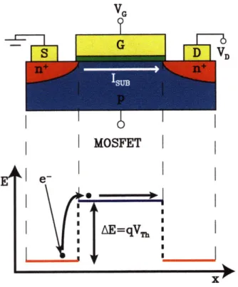
Static power arises from power dissipation of a MOSFET during periods when switch-ing does not occur and is thus always present. Although there are several contributors to static power dissipation the two most significant sources are gate current leakage when the MOSFET is turned "on", Figure 1-5a and subthreshold current leakage when the MOSFET is turned "off," Figure 1-5b.
1.1.3.1 Gate Leakage
The requirement from Section 1.1.1 for our MOSFET, that CG > Cs, implies that that the to, < L. As the length scale of devices decrease so does the thickness of the oxide, eventually leading to the point where t,, is thin enough that there is direct tunneling of electrons from the gate to the channel upon an applied bias, VGS.
This results in the gate leakage that increases exponentially as the oxide thickness is continually decreased and the contribution to the state power dissipation can be quite significant. Recent breakthroughs in high-k dielectric have brought gate leakage under control. This can be understood by considering the gate-channel capacitance to be a parallel plate capacitor, and whose capacitance can be modeled by the following equation:
kcoA
C = (1.7)
where k is the relative dielectric constant of the material between the plates, EO is the permittivity of free space, and A is the area of the capacitor. Then relative to
SiO2 with a k=3.9, if a material with a higher dielectric constant such as Hf 02 with
a k-25, and assuming that the capacitance needs to remain the same or better then the following equation can be obtained for an equivalent thickness of H
f02:
kHfO2
tHfO H tsoz (1.8)
tH f02 tSi0 2
Since kHfO2 > 6 x ksio, the gate thickness is much greater than there is a drastic decrease in gate leakage for an equivalent capacitance. This is problem that for the most part can be overcome with selection of different materials.
1.1.3.2 Subthreshold Leakage
The second source of leakage is the subthreshold current leakage and with the break-through in new high-k dielectric materials discussed in the previous section is seen as the performance limiting issue in future electronics. [1] Subthreshold current leakage can be explained by examining the conduction bands of a MOSFET like an NMOS in Figure 1-6. As a note, the analysis in this section assumes that the MOSFET is ideal, meaning that, again, control of the channel is dominated by capacitance the between the gate and the channel.
In a perfect world, in the "off" state the electrons would not move between the source and drain because of the energy barrier between the source and channel, in practice this is not the case and will be discussed shortly. The way this channel switches on and off is by lowering the channel energy level, through the application of a gate-source bias, low enough such that the energy level of the channel matches that of the source and drain allowing the electrons to easily flow. The voltage necessary to achieve this condition is the threshold voltage, Vth and is something designers would like to drive down because of it's relation the supply voltage, VDD, and in turn dynamic power.
elec-VG
MOSFET
I
..
i
Figure 1-6: An NMOS and the corresponding conduction band energy diagram.
trons, Ne are excited above this energy barrier resulting in the subthreshold leakage. The likelihood that an electron in the source will be able to hop the barrier is given by Boltzmann statistics giving an leakage current:
Sub Ne exp exp (qVTh (1.9)
This is the origin of the subthreshold leakage.
Of course, as VGs increases from 0, more and more current will flow until VGS =
VTh. (Figure 1-7) The slope, S, as the current is increasing in the subthreshold region
is defined as:
S /GS/1Og0 1 (I)
= -kT/qloglo(I) (1.10)
= 60mV/decade
The slope thus defines a fundamental limit for the subthreshold leakage in field effect transistor and as previously stated is governed by the Boltzmann statistics of
0
Leakage
current Subthreshol d region
T VGS
Figure 1-7: Plot of the source-drain current as a function of gate-source bias. a single electron.
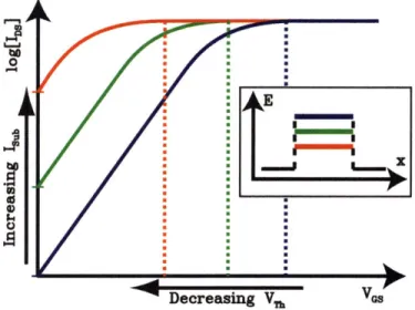
Why is this important'? If the overall goal is to drive down the total power consumption, than from a dynamic power consumption stand point it is important to drive down the supply voltage and also decrease the threshold voltage. The threshold voltage is decreased by altering the energy barrier through means such as doping. From Figure 1-8, a decrease in threshold voltage results in an increase in leakage. So it is then left up to designers to come up with a balance between dynamic and static power loses. The ideal solution, seen in Figure 1-9, is to increase the subthreshold swing, or decrease the slope, and therein have the ability to decrease the threshold voltage while maintaining or potentially decreasing the subthreshold leakage through the device, and in turn decrease the power dissipation of the device as a whole. Of course, as previously discussed, the 60 mV/decade is a fundamental limit and is not a parameter that is tunable in current MOSFETs or any such electrostatically modulated devices with independent charges.
1.2
Fundamental Limits of Power Dissipation
Having set some basic limits on power dissipation by logic devices based on CMOS, is is important to set a lower bar to power dissipation by understanding what are
/
Decreasing Vr V,
Figure 1-8: Plot of the source-drain current as a function of gate-source bias for various Vth.
Decreasing Vr
Figure 1-9: Plot of the source-drain current as a function of gate-source bias for various S.
source drain
gate
source drain
gate (b)
Figure 1-10: Comparison of a) conventional single molecule FET to that of a b) mechanical single molecule FET
the fundamental limits in power dissipation to computational logic in general. The minimum energy dissipated per bit will be briefly considered from a statistically mechanics arguments. Considering the use of binary logic, then the each bit used for computation can exist in one of two 2 states, either 0 or 1. Thus, a change in entropy of a single bit is given by S = kb ln (2). Thus, the minimum switching energy per bit in any logic device is given by Equation 1.11 for any device including both NEM devices and conventional field effect transistors (FETs).
Emin kBTl In (2) (1.11)
This the limit is known as the Shannon-von Neumann-Landauer (SNL) limit. [73] This highlights the fact that the limits in power dissipation in CMOS are not fundamental to the limits in power dissipation to computation, but limited to CMOS
1.3
Case for NEMs
1.3.1
General Theory
In their theoretical work, Ghosh et al. [18] considered the limits of transconductance, and hence power dissipation, on the molecular scale, what some would consider the ultimate end of the roadmap in terms of scaling. From Equation 1.11, it is appar-ent that the scaling limits in CMOS power dissipation are limits in the design and architecture of electrostatically operated device, and therefore it was considered that any device that was electrostatically actuated would have the same limits. Therefore, a molecular device like the one in Figure 1-10a, whose current I is modulated by induction of charges via a gate voltage, V will, at best, have transconductance per unit current, gm/I, of:
9 _ (1.12)
I kT
Where q is the electron charge which, again, is the limit of a standard FET transconductance obtained in Section 1.1.3.2.
It is logical then to consider devices that operate by alternative means, such as mechanical actuated transistors. Let a device now be considered whose current is modulated by a gate voltage, V, induced confornational change like the one in Figure 1-10b, where the gate field interacts with the molecular dipole, p, the transconduc-tance per unit current, is now at best:
9gnf (1.13)
I kT t
where t is the length of the molecule. For a molecular dipole where there is no net molecular charge, the term /t = q, meaning that equation 1.13 becomes:
conf es
gf q g
I kT I
me-chanical transistors. This does not mean that from even this stand point meme-chanical transistors are not of interest, since they still offer an alternate route towards achiev-ing the limits of transconductance.
1.3.2
Potential Solution
Since there is no net benefit to mechanical transistors when there is no net charge, what happens in the case where there are a surplus of charges? An archetype me-chanical transistor, shown in Figure 1-11, consisting of a conducting actuator, which acts as a conventional channel, that is brought in and out of contact between the source and drain via a gate-field induced conformational change is considered for this discussion. In the case of a simple dipole, Figure 1-11a, the mechanical actuator is turned from the "off" to "on" positions by an applied bias threshold VT or VG. The difference in energy between the two positions is just (qV. The subthreshold slope limit is thus the same for this device and a MOSFET. Now consider a device that moves between the same two energy states as before, but instead of moving a single charge, there are now three charges that need to be moved, Figure 1-11b. Because
the energy difference in the two devices are the same, i.e. AEl-ch9 = AE3-ch, then
Vth,3chg = Vth,lchg meaning the subthreshold slope of the mechanical device with
three charges is 5 that of a device containing 1 charge, or that of a MOSFET. This same idea can be applied to a system with Z charges, allowing for subthreshold slope decreases by a factor of . Conceptual this is very promising, but are there any devices or systems where this actually occurs, i.e. where multiple charges lead to a reduction in subthreshold slope'? The answer to this question is found in biology in the form of voltage-gated ion channels.
1.3.3
Ion Channels
Voltage-gated ion channels are transmembrane ion channels that open through me-chanical actuation of their voltage sensing helices by an applied bias across the imem-brane that enables the flow of ions through the channel. These systems provide a
Conducting x Actuator
Source
Drain
on' (a) "off"
11Charges
-.MHinge
I-oi" (b) off"
Figure 1-11: Mechanical Relay
system to investigate the influence of multiples charges for low voltage switches due to the fact that the helices themselves contain multiple positive charges that enable extremely low operating voltages. A schematic and diagram of a voltage gated potas-sium ion channel is shown in Figure 1-12. [30] The conductance versus voltage data for these voltage gated ion channels is shown in Figure 1-13. [23] Indeed, ion channels are able to switch with subthreshold slopes of 15 mV/decade, 4 times less than the 60 mV/decade limit of MOSFETs. This evidence shows the ability of multiple charges employed in an electromechanical based system towards the creation of devices that that exhibit low subthreshold slopes..
1.4
Our approach to address these problems
The purpose of this thesis is to create a test bed device for mechanical transistors with the future goal of being used to create devices that exhibit these low subthreshold
open II 1 I I I
I I
I 1I~
1
I I
I 1I
iI
Figure 1-12: Voltage dependent K+ channelSub hreshold I reion Axon 17 20 21 21 I I I Temp. 6 6 8-5
\ I(( d
I
I
'8 5I
I I -120 -110 -100 -90 -80 -70 -60 -50 -40 0I Closed -30 -20-10 0Displacement of membrane potential (mV.)
Figure 1-13: Data for a voltage gated ion channel. Hodgkin and Huxley, J. Physiol. 116, 449 (1952a) 38 Open I 01 001 0001 L S I I - I
I
closed / ( I (J'JIL" (41illIk
b ~ r cc ic it p c L v ....II
U0 ,t ,1.4.1
Carbon Nanotubes
The most important consideration in creating a mechanical transistor is the selection of the material for the conducting actuator. In order to ensure a large on-off ratio the actuator needs to be highly conductive. Mechanically, the actuator needs to be able withstand multiple switching events without failure and therefore needs to be a very strong materials. Since it is desired to have a high integration density, the material should have both of these properties while having the physical size at the molecular scale. With the desire of creating a device that has multiple charges like an ion channel in the future, using a material that is functionalizable is highly desired.
Carbon nanotubes/fibers (CNs) are promising as a material for NEMs because of their exceptional and unique electronic, mechanical, and chemical properties. Es-sentially CNs are rolled sheets of graphene formed to create a tube, hence the name carbon nanotube, Figure 1-14. Their diameters can range from 2-300nm making them compatible with modern and future MOSFET integration. Electrically, CNs are highly conductive and can carry an electrical current density of - 4 x 10⁹Acm -2 ,
several orders of magnitude greater than that of copper or alhminum.[24] Mechani-cally, with a Young's Modulus ranging from 0.8 to 1 TPa, carbon nanotubes are the strongest known material. [68] Finally, opening up the ends of CNs in an oxidizing en-vironment allows them to be functionalized with a large library of carboxyl (COOH) functional groups. [67]
In addition to all this, they have been well studied in terms of their synthesis [63] and have been used to create electromechanical devices such as actuators [3], tweezers [36], and even memory elements [59]. Hence, carbon nanotubes/fibers are the ideal candidate for NEM switches.
1.4.2 Device
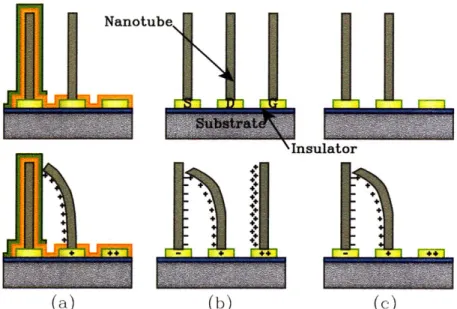
The proposed device that's investigated in this thesis is a vertically oriented carbon nanotube/fiber (CN) based relay (VOCNR) shown in Figure 1-15. The device consists of a vertically oriented CN based actuator that is electrically connected to a substrate.
x
Graphene
I!
Carbon Nanotubes
Figure 1-14: Structure of a carbon nanotube from a sheet of graphene.
Situated on either sides of the CN are contacts that are electrically isolated from each other as well as the CN. A schematic of the device under operation is shown in Figure 1-16. The envisioned as grown device begins with the CN mechanical actuator situated in the center of the two contacts, Figure 1-16a. A bias is applied between the CN and one of the contacts and the device is turned on when the voltage is large enough to pull the CN into electrical connection with the contact, the voltage at which this occurs in the pull-in voltage, Vpi, Figure 1-16b. The CN then remains connected to the contacted because of small scale van der Waals forces, Figure 1-16c. An bias applied between the CN and the opposing contact turns the device off when the device is pulled into the opposing contact, the voltage at which this occurs is the pull-off voltage, Vpo, Figure 1-16d.
1.5
Thesis Overview
In Chapter 2 the theory and design of the VOCNR are discussed. First, a basic continuum model of these relays is examined in order to understand device scaling as it relates to the pull-in voltage. After understanding the basic operating principles
Contacts
Figure 1-15: Proposed device for studying nanoelectromechanical systems
- Drain
+,
=P
D=
jai n
r-
(a)
/
(b)(c) (d)
of the device the issues as they are related to previous works in this area are looked at, in particular is the issue of stiction in NEMs. Last, are the ways these issues are addressed by the design of a NEMs relay presented in this thesis.
In Chapter 3 the initial prototyping and first generation fabrication efforts are discussed. First, an overview of the first generation architecture and fabrication route to a vertically oriented carbon nanorelay is given. The virtues of the architecture and fabrication in terms of performance criteria as well as potential pitfalls are also given. Second, a proof of concept experimental setup is described and the results are given. Last, a set of experiments utilizing the proof of concept setup and initial fabrication efforts is described followed by results and a discussion.
In Chapter 4 a fully wafer integrated vertically oriented or vertical carbon nanore-lay is discussed. Fabrication issues such as limitations in nanotube and oxide growth via PECVD are examined. A novel self-aligned technique for creating precisely aligned gaps to vertical structures is presented. Results are analyzed to demonstrate device scaling. Finally, pull-in data for a device is shown and related to limitations in fab-rication.
In Chapter 5 a new type of electromechanical switch fabricated from two layers of graphene films grown via aumbient pressure chemical vapor deposition also called a double graphene switch is discussed. This includes the design and fabrication of the device as well as the electrical and electromechanical characterization of the double graphene. Finally the failure of the device due to mechanical tearing of the graphene is shown.
In Chapter 6 conclusions regarding both a vertical carbon nano-relay and a double graphene switch are presented. This is mainly meant to highlight some of the virtues as well as pitfalls in the overall work in this thesis.
Finally, in Chapter 7 future avenues of suggested research for both devices are presented. This includes, but is not limited to, the optimization of the vertical carbon nanorelay for wafer integrated pull-off operation and the scaling the double graphene switch to enhance the mechanical robustness of the device.
Chapter 2
Theory and Design
2.1
NEMs Relay: Continuum Model
The continuum modeling of a CN based NEMs relay follows from the works of Desquenes et al. [12] A complete and in-depth model for CN based relays can be found in a variety of references. [12, 37, 13, 71, 21] In large part these models are validated by considering how they compare to molecular dynamics models and few experimental devices, and have shown good correlation between the both. In general the difficulty in modeling NEMs is not the accuracy of the model, but in the wide variations in the properties of the nanostructures they are modeling. As an examples, the elastic modulus of carbon nanotube and nanofibers can vary by upwards of about two orders of magnitude depending on, amongst other characteristics, the diameter [60, 41], structure [39], and growth method [46]. In this thesis only a basic model in-volving the static behavior, or more specifically the pull-in behavior, of carbon based NEMs will be considered for the purpose of understanding device scaling. As such, the validity of a continuum mechanics model for the primary device of this thesis, the vertical carbon nano-relay, will be partially proven by considering the scaling behavior of a measurable parameter, such as gap size, of a single device (Section 4.3.1).
Although the analysis will primarily focus of vertical carbon nano-relays with a cantilever type structure, schematically shown in their "on" and "off " states in Figure 2-la and 2-1b, respectively; the analysis technique can also apply to relays
Electrostatic
g - Elastic
ICg d van der Waals 0
L Insulator -Contacts +
(a)
(b)
Contacts L Insulator + VP Electr (c) (d)Figure 2-1: Forces involved in a carbon nano-relay. Schematic of: a) an vertical carbon nano-relay showing relevent dimensions. b) an activated vertical carbon nanorelay showing relevent forces. c) a horizontal beam relay showing relevant dimensions and d) an activated horizontal beam relay showing relevent forces
that are dual clamped as in a horizontal beam device schematically shown in their
"on" and "off" states in Figures 2-1c and 2-1d, respectively. The basic principle to
solving the static behavior of a CN based relay is a simple balance of forces when either device is actuated by an applied bias. When a bias is applied between the CN cantilever or possibly even a graphene beam and an electrode several forces act on the electromechanically actuating the cantilever or beam. There are electrostatic and to a lesser extent van der Waals forces that cause deflection of the actuator towards the conducting electrode and elastic restoring forces opposing the deflection of the beam. In addition, the analysis will consider both the case of MWCNT or large carbon nanofibers with cylindrical cross sections with outer diameters, d, as well as the case of a graphene sheet with a width and thickness of w and t respectively.
2.1.1
Van der Waals
The van der Waals interaction between the CN and the contact is modeled by the Lennard-Jones potential [44]
VR VA
R VA (2.1)
where rij is the distance between ith and jth atoms, VR is the repulsive constant, and VA is the repulsive constant. By following the model in by Desquenes et al. [12] The van der Waals interaction force can be written as:
7 VRp2wL 1 ( )) (2.2)
FvdW = (2.2)
for a rectangular beam, or
V
V7VRp2dL 1 1d) (2.3)
FvdW (2.3)
6 g3 (g + d)3
for a cylindrical beam, where p is the atomic density, L is the length of the actuator and g is the gap size. Although the van der Waals forces are written here for completeness, they will be ignored in the final analysis, because of their insignificant contribution to pull-in which occurs at relatively large gap sizes, gpull-in = 5gi, where
gi is the initial gap size, [61] as well as the relatively large size CNs used in this thesis.
2.1.2
Electrostatic
The electrostatic or capacitive force is easily derived by considering the electrostatic force, Fsec, felt by a single charge, q, in electric field, E, is written as
Fs,eiec = qE (2.4)
Then for a device with multiple charge, Q, in an electric field the total electrostatic force, Feec is equal to
Fete = QE (2.5) If in either case of an beamn or a cantilever the device acts like a parallel plate capacitor, that the total nnmber of charges Q on the capacitor is given as:
EoAcV
Q
= (2.6)g
where Eo is the permittivity of free space, Ac is the area of the capacitor, and V is the applied voltage. The electric field is written as:
V
E = (2.7)
g
Combining Equations 2.5,2.6, and 2.7 the following equation is derived for the electrostatic force:
1 oAV 2
Felec,cy -2 g2 (2.8)
Again for simplicity, assume that a cylinder has more or less the area of a rectangle, then:
1 EodLV2
Felec,re 2 g2(2.9)
and for a rectangular beam:
1 cowLV2
Feiec = 2 g2 (2.10)
2.1.3
Elastic
In it's equilibrium state a beam or cantilever remains in an undeflected state, therefore in order to deform that beam or cantilever an elastic force related to the spring constant, k, and deflection distance Ag must be applied in order to deform the beam. Since every action has an equal and opposite reaction, the equal and opposite reaction
is the elastic repulsive force and is given by:
Felas = kAg (2.11)
The spring constant, k, depends on the material and geometry of the actuator. For a cantilever type device the spring constant is given as:
EI
kcan = 8 , (2.12)
and for a double clamped beam the spring constant is:
EI
kbeam = 384 LLa
where E is the modulus of elasticity and I is the moment of inertia.
(2.13)
Again, the moment of inertia is a function of the geometry of the beam and is defined for a cylinder as:
Icy - (2.14) and for a rectangular prism as:
wt3
12 (2.15)
The following equations are obtained for the elastic forces of a cantilever with cylindrical cross section:
7rd4E
Felas,can,cy 8L3 Ag
8V" (2.16)
and for a beam with a rectangular cross section:
Felas,beam,re
-32wt3E
2.1.4
Pull-In Scaling
Pull-in occurs when Feec = Fas for a gap [61]:
9PI = 29i (2.18)
3
By the above equations for various geometries the following relations are obtained for the pull-in voltage, Vpj, as a function of the geometry of the actuator and gap size, for a cylindrical cross section
VpI,cy oc L4 (2.19)
and for a rectangular cross section:
i Et3g3
VpIre oc (2.20)
Equations 2.19 and 2.20 provide general guideline for device design as it relates to scaling of the operating voltage of a nanorelay.
2.2
Previous Approaches
Several approaches have been implemented in discovering a route towards a carbon nanotube/fiber based NEMs. Although each approach has been successfully em-ployed, limitations in their design and fabrication prevent them from being a practical replacement for CMOS. The issues of these designs thus far has been stiction, both in the creation of a horizontal and vertical design, and finally alignment of contacts with respect to the carbon nanotube. Of these two flaws, stiction is the most crucial as it is a fundamental problem, rather than a limitation in fabrication, and will be reviewed in Section 2.3.


![[Lysophosphatidic acid: a "bioactive" phospholipid]](data:image/gif;base64,R0lGODlhAQABAIAAAP///wAAACH5BAEAAAAALAAAAAABAAEAAAICRAEAOw==)