HAL Id: tel-01586070
https://tel.archives-ouvertes.fr/tel-01586070
Submitted on 12 Sep 2017HAL is a multi-disciplinary open access archive for the deposit and dissemination of sci-entific research documents, whether they are pub-lished or not. The documents may come from teaching and research institutions in France or abroad, or from public or private research centers.
L’archive ouverte pluridisciplinaire HAL, est destinée au dépôt et à la diffusion de documents scientifiques de niveau recherche, publiés ou non, émanant des établissements d’enseignement et de recherche français ou étrangers, des laboratoires publics ou privés.
quantum dots
Andrea Corna
To cite this version:
Andrea Corna. Single spin control and readout in silicon coupled quantum dots. Quantum Physics [quant-ph]. Université Grenoble Alpes, 2017. English. �NNT : 2017GREAY003�. �tel-01586070�
DOCTEUR DE la Communauté UNIVERSITÉ
GRENOBLE ALPES
Spécialité : Physique de la Matière Condensée et du Rayonnement
Arrêté ministériel : 7 Août 2006
Présentée par
Andrea Corna
Thèse dirigée par Marc Sanquer et codirigée par Xavier Jehl
préparée au sein du laboratoire de transport électronique quantique et supraconductivité,
du service de photonique electronique et ingénierie quantiques, de l’institut nanosciences et cryogénie,
du CEA Grenoble
et de l’école doctorale de physique de Grenoble
Single Spin control and readout in
silicon coupled quantum dots
Thèse soutenue publiquement le 20 Janvier 2017, devant le jury composé de :
Hervé Courtois
Université Grenoble Alpes et Institut Néel/CNRS, Président
Gwendal Fève
Laboratoire Pierre Aigrain/ENS Paris, Rapporteur
Dominique Mailly
Centre de Nanosciences et de Nanotechnologies/CNRS et Université Paris-Sud, Rapporteur
Marc Sanquer
PHELIQS/INAC/CEA et Université Grenoble Alpes, Directeur de thèse
Xavier Jehl
Abstract
In the recent years, silicon has emerged as a promising host material for spin qubits. Thanks to its widespread use in modern microelectronics, silicon technology has seen a tremendous development. Realizing qubit devices using well-established complementary metal-oxide-semiconductor (CMOS) fabrication technology would clearly favor their large scale integra-tion. In this thesis we present a detailed study on CMOS devices in a perspective of qubit operability. In particular we tackled the problems of charge and spin confinement in quan-tum dots, spin manipulation and charge and spin readout.
We explored the different charge and spin confinement capabilities of samples with differ-ent sizes and geometries. Ultrascaled MOSFETs show Coulomb blockade up to room tem-perature with charging energies up to 200 meV. Multigate devices with larger geometrical dimensions have been used to confine spins and read their states through spin-blockade as a way to perform spin to charge conversion. Spin manipulation is achieved by means of Electron Dipole induced Spin Resonance (EDSR). The two lowest valleys of silicon’s con-duction band originate as intra and inter-valley spin transitions ; we probe a valley splitting of 36 μeV. The origin of this spin resonance is explained as an effect of the specific geometry of the sample combined with valley physics and Rashba spin-orbit interaction. Signatures of coherent Rabi oscillations have been measured, with a Rabi frequency of 6 MHz. We also discuss fast charge and spin readout performed by dispersive gate-coupled reflectometry. We show how to use it to recover the complete charge stability diagram of the device and the expected signal for an isolated double dot system. Finite bias changes the response of the system and we used it to probe excited states and their dynamics.
Résumé
Au cours des dernières années le silicium est apparu comme un matériau hôte prometteur pour les qubits de spin. Grâce à la microélectronique moderne, la technologie du silicium a connu un formidable développement. Réaliser des qubits utilisant la technologie bien établie de fabrication CMOS de semi-conducteurs favoriserait clairement leur intégration à grande échelle. Dans cette thèse nous présentons les travaux effectués dans une perspective des qu-bits CMOS. En particulier, nous avons abordé les problèmes de confinement des charges et des spins dans les boîtes quantiques, la manipulation des spins et la lecture des charges et des spins.
Nous avons exploré les différentes propriétés de confinement de charge et de spin dans des échantillons de tailles et de géométries différentes. Les MOSFETs de taille extrêmement ré-duites montrent du blocage de Coulomb jusqu’à température ambiante, avec des énergies de charges jusqu’à 200 meV. Les dispositifs multi-grilles avec des dimensions géométriques plus grandes ont été utilisés pour confiner les spins et lire leur état par blocage de spin, en réalisant ainsi une conversion spin / charge. La manipulation des spins est réalisée au moyen d’un dipôle électronique induisant la résonance de spin (EDSR). Les deux plus basses vallées de la bande de conduction du silicium sont visibles sous forme de transitions de spin intra et inter-vallées. Nous observons une levée de dégénérescence de vallée d’amplitude 36 μeV. La résonance de spin que l’on observe résulte de la géométrie spécifique de l’échantillon, de la physique des vallées et de l’interaction spin-orbite de type Rashba. Des signatures de mani-pulation cohérente, sous forme d’oscillations de Rabi, ont été mesurées, avec une fréquence de Rabi de 6 MHz. Nous discutons également de la lecture rapide des charges et des spins effectuée par réflectométrie dispersive couplée à la grille. Nous montrons comment l’utili-ser pour reconstruire le diagramme de stabilité de charge du dispositif et le signal attendu pour un système à double boîte isolé. La tension de polarisation finie modifie la réponse du système et nous l’avons utilisée pour sonder les états excités et leur dynamique.
Introduction 1 1 Single Electron Transistor from low to Room temperature 5
1.1 Devices fabrication . . . 6
1.2 Results . . . 8
1.2.1 Single dot device . . . 8
1.2.2 Double dots device . . . 12
1.3 Role of surface roughness . . . 14
1.4 Conclusions . . . 16
2 Spin manipulation 17 2.1 Device . . . 17
2.1.1 RF antenna . . . 19
2.1.2 Selection . . . 26
2.2 Setup and device connection . . . 30
2.3 Stability diagram and bias spectroscopy . . . 32
2.4 Magneto-transport and spin blockade . . . 35
2.4.1 Spin blockade theory . . . 35
2.4.2 Lifting of spin blockade . . . 38
2.4.3 Magnetotransport measurements . . . 42
2.5 Electron Dipole-induced Spin Resonance . . . 45
2.5.1 Relaxation phenomena and Bloch equations . . . 48
2.5.2 Continuous-Wave Spin Resonance . . . 48
2.6 Spin-Valley Resonance . . . 56
2.6.1 Spin-valley blockade . . . 61
2.7 Towards coherent control with EDSR . . . 63
2.7.1 Setup and calibration . . . 65
2.8 Origin of EDSR . . . 68
2.8.1 Permanent magnetism . . . 68
2.8.2 Spin-Orbit and Valley mixing modelling . . . 69
2.8.3 Tight-binding results . . . 73
2.9 Conclusions . . . 75
3 Reflectometry - Dual-channel gate dispersive readout 77 3.1 Device and measurement setup . . . 78
3.2 Dispersive readout signal . . . 80
3.3 Results . . . 81
3.4 Modeling of out-of-equilibrium response . . . 82
3.5 Conclusions . . . 87
Conclusions 89 Bibliography 93 Appendix A Device fabrication 105 A.1 Fabrication steps . . . 105
A.2 E-beam/DUV hybrid lithography . . . 110
Appendix B Device selection 113 B.1 Probe station . . . 116
In recent years quantum computing has gone through a massive development and widespread interest. The key element of an architecture for a quantum computer is the qubit, the quantum analogous of the classical boolean bit. In these thesis we will study some key technologies and phenomena to possibly build a qubit in a scalable silicon spin quantum architecture. In particular we will analyze the aspect of spin and charge confinement, manipulation and read-out.
Recently several quantum computer architectures have been proposed and realized. The point is to find materials and engineer a system where qubit can be physically realized, ini-tialized, controlled, read and coupled together to implement quantum algorithms on top of them. Due to the intrinsically probabilistic nature of quantum mechanism and unavoidable decoherence phenomena, error correction is an import part of an architecture to obtain a fault-tolerant computation. A qubit is essentially a quantum two-level system, so any system in which we can select a subset of level, initialize to a known state, manipulate and read is a possible candidate. Possible candidate are the polarization of a photon [1], the spin of an electron [2] or a nucleus [3], a charge position [4], magnetic flux [5] or many others. All these system can live on a different platform, like trapped ions [6], molecules probed by Nu-clear Magnetic Resonance [7], superconducting circuits, color centers in diamonds, dopants or quantum dots in semiconductors.
Solid states system have the great advantage to make possible the realization of very compact qubits and possibly scalable architectures. Superconducting qubits[8] have achieved great advancements in terms of coherence time, fidelity and scalability[9], realizing also quantum computer prototypes with few qubits [10, 11].
Another promising architecture is represented by spin qubits in semiconductors. qubits are made by one or more spins confined in a quantum dot or a dopant in a semiconducting sub-strate. The size of these objects is very small, thus enabling a large scaling needed for a real quantum computer. Moreover the semiconductor technologies developed for micro and nano electronics provides an advanced and well-established technological platform.
heterostruc-tures [12–14]. Two-dimensional electron gas in Gallium-arsenide quantum-well has a great electron mobility and low-electron density, so it’s easy to locally deplete the gas and define very tunable quantum dots [15]. However, gallium and arsenic have a non-zero nuclear spin, so thought hyperfine interaction with the trapped electron, they induce decoherence.
By contrast silicon has a much lower concentration of non-zero nuclear spins and it can be isotopically purified to to achieve extremely long coherence times [16]. Moreover there is a larger knowledge and technology available for the fabrication, thanks to the development in the microelectronic industry. On this purpose we recently realized the first qubit employing a CMOS (Complementary Metal-Oxide-Semiconductor) industry-standard fabrication pro-cess [17]. This pave the road for a possible integration with driving and readout electronics on-chip [18]
The goal of this thesis is to study and develop the building blocks to realize a quantum com-puter in a silicon CMOS platform. In particular, we focused on the aspect needed to realize a single qubit using MOSFET-like structures made with the Trigate Silicon-On-Insulator technology [19]. In this manuscript we investigate how to create silicon quantum dots of different sizes and confine charges. We will look also how to bound and probe a specific spin with spin blockade and how to rotate the spin orientation with Spin Resonance. Finally we explore how to probe the charge and spin states thought dispersive readout with the goal of a fast readout.
Contrary to the qubit reported in [17] which employs the spin of an hole, we will focus on the electron spin. The behavior of electrons in silicon have been intensively studied [20] and their physics is well known. On the contrary holes have been investigated less and building good low-temperature devices is more challenging [21, 22]. Their small mobility leads to an higher sensibility to surface roughness and the higher Spin-Orbit Interaction can increase the coupling to charge noise.
Contents
In chapter 1 we will investigate the behavior of ultrascalated silicon MOSFET. We present the peculiarities of the fabrication process to achieve very small dimension and the room-temperature pre-characterization process. We study the electrical behavior in a wide range of temperature, from room temperature down to 300mK. The different confinement mechanism are investigated and a model is proposed. Coulomb blockade with large charge energies is obtained for system with one or two dot in series, in selected case even up to room temper-ature.
In chapter 2 we investigate spin manipulation through spin resonance. We show a sample geometry tailored for this purpose and how mass-characterize it at room-temperature. We simulate the microwave behavior of the on-chip antenna and how it can be used to drive spin resonance. Low temperature measurement are used to investigate spin blockade as a way for spin initialization and readout. We show signature of spin resonance and the effect of the valleys in the silicon conduction band. A theoretical model with numerical simulation is presented to explain the origin of the resonance signal. Selected measurement of a possible coherent spin manipulation (Rabi oscillation) are also presented.
Finally in chapter 3 we study gate coupled dispersive readout as a mean to perform sensitive readout of a double dot system. We explain how dispersive readout works, how to imple-ment it and what it probes. We show charge stability diagram of the double dot system and all the charge transitions that take places. A model to explain the specific features of the recorded lineshapes is proposed. We employs this model to derive the charge dynamics and the relaxation rates between excited and ground state.
In appendix A we show the Trigate fabrication process. We explain its peculiarities and the modifications in the process flow to tailor it for quantum devices.
In appendix B we briefly explain the room-temperature selection process and the semi-automatic probe-station used for that purpose.
Single Electron Transistor from low to
Room temperature
The quest for electronic circuits using single atoms and molecules took off with the rise of nanosciences. Atom switch [23], single atom contact [24], single atom transistor [25–28, 20] are various examples of nanodevices where the electric current is driven through the atomic orbitals of a weak link in an elementary circuit. Despite proof of concept demonstrations, these objects still suffer from many drawbacks: they are very fragile and their interfacing to the macroscopic world is extremely challenging. Most of them can hardly be integrated into standard, scalable semiconductor processes, and reveal their atomic properties only at low temperature.
On the other hand, reliable silicon CMOS transistors become smaller and smaller. The most advanced design to date is the nanowire (NW) CMOS transistor which consists of an etched quasi-one dimensional undoped silicon channel covered by a gate and connected to the heavily doped source and drain contacts. Nanowire transistors have better immunity to short-channel effects than Fin-FET and planar transistors thanks to the very good elec-trostatic control of the channel by the gate. Because this NW transistor benefits from the maturity of silicon processing and technology, it is attractive to use it as a platform for a room temperature single artificial atom (AA) transistor, i.e. a tiny channel where carriers are strongly confined in all 3 dimensions and controlled one-by-one by gates. Such AA shall display the excellent features inherited from the CMOS fabrication: established technology with no use of an expensive electron beam lithography, standardization and mass production, steady improvement in materials and processes, etc.
Here we present such an artificial atom transistor, tunable with a combination of top gate and backgate voltages, for which the atomic-like features can be tracked continuously from low to room temperature. This CMOS artificial atom exists in both 𝑛- and 𝑝-type transistors.
The design combines small diameter channel (3.4 nm) and long (25 nm) spacers separating the gate (G) from the heavily doped source (S) and drain (D) electrodes, in order to enhance confinement and Coulomb interactions. Despite the very small size of these artificial atoms (a few nanometers) the fabrication is massively parallel. Although the process variability is large at this scale, several working samples have been already produced. This chapter is an extract of our article “Quantum dot made in metal oxide silicon-nanowire field effect transistor working at room temperature” [29].
1.1 Devices fabrication
Top-down silicon NWs [30] as well as Chemical Vapor Deposition (CVD) grown silicon nanowires [31, 32] have both reached the 2 to 8 nm diameter range. These devices show strong transverse confinement thanks to the small cross-section of the NW. Isolation from the S-D contacts by longitudinal confinement is then the key to reach the AA regime where the interplay between Coulomb blockade and quantum confinement regulates the addition spectrum. For CVD grown silicon NWs, the S-D contacts are usually Schottky barriers be-tween metallic electrodes and the nanowire [32, 33]. Here instead of Schottky contacts we used highly doped silicon contacts (source and drain), and decoupled them from the channel by introducing 25 nm long intrinsic silicon nanowire spacers (non-overlapped S-G geome-try). These spacers play the role of long linker molecules in single atom transistors [25]. The transmission through the spacers can also be controlled by the substrate bias. A quantum dot is formed below the gate by the electric field, and it accumulates electrons (or holes) [34, 35]. Overall, these spacers present several advantages. First, they preserve the electrostatic con-trol over the channel – and therefore the AA tunability – even at short gate lengths (10 nm). Second, they limit the screening of the electron interactions by the S-D electrodes. Third, they prevent the lateral diffusion of source and drain dopants in the channel. Fourth, it has been shown that long and thin resistors are more efficient than thin tunnel barriers to prevent parasitic cotunneling in metallic single electron transistors [36]. This is reminiscent of using quantum point contacts [37] or resistive circuits [38] in order to observe charging effects and Coulomb blockade [39].
Specifically, our AAs are made in thin (≈ 3.4 nm diameter) etched nanowires (see fig-ure 1.1). An omega-shaped gate (Ω-gate) sets the transverse electric field locally. The fabri-cation process is similar to the one explained in appendix A. E-beam lithography has not been employed, only standard DUV 193 nm deep-UV (DUV) lithography has been used. Follow-ing the nanowire patternFollow-ing, a resist trimmFollow-ing process is performed in order to reduce the NW width down to 10 nm. A 7 nm thick oxidation further reduces their diameter down to
a
c
b
d
Figure 1.1 Geometry, simulations a) TEM image showing the cross section of the 3.4 nm diameter silicon nanowire, the 7 nm thick SiO2gate oxide, the 1.9 nm HfSiON and the 5 nm ALD TiN/poly Silicon gate. b-d) Models used for the simulations b) A 𝑛-type device with moderate surface roughness (wire diameter 3.4 nm; surface roughness rms Δ = 0.25 nm). Silicon is in red, SiO2in green, HfO2(HfSiON) in blue, TiN gate in grey, Si3N4otherwise. The silicon substrate is not represented. The white dots are arsenic donors in the source and drain. This device has a charging energy around 90 meV. c) A 𝑛-type device with strong surface roughness secluding a 4 nm long dot under the gate. d) A 𝑝-type device with strong surface roughness secluding a 7 nm long dot under the source spacer, and a very long, ∼ 30 nm long dot under the gate and drain spacer.
≈ 3.4 nm and protects the wires for the rest of the fabrication. Pattern edge roughness be-comes increasingly important as the features become smaller. The line-edge and line-width roughness of the patterns directly result from the initial roughness of the resit. This is signif-icant after resist trimming, with the formation of several constrictions and possibly quantum dots. Other fabrication steps are identical. Devices are simple MOSFET structures with only one gate. Spacers are 25 nm long.
This integration scheme based on a CMOS process allows for an easier implementation of contacts, spacers, top and bottom gates – all crucial building blocks of a reliable artificial atom. Although room temperature single electron transistors have already been reported in
small silicon structures [40–43] and have been constantly improved up to date [30, 44], none of the previous demonstrations used standard CMOS integration and – with the exception of Ref. [45] – all of them were fabricated with e-beam lithography.
Figure 1.1a shows a TEM image of the cross-section of a device while Figs. 1.1b-d show structural models used for electrical simulations. The line-edge roughness of the patterns is critical at this scale and directly results from the initial roughness of the resist (see figure S1 in the supporting information). Figs. 1.1b-d are therefore possible scenarios for the ex-perimental data discussed below: a moderate surface roughness disorder (b); and a strong surface roughness defining a quantum dot either below the gate (c) or below the spacers (d).
1.2 Results
We present here the results of two different measured samples. Both of the devices shows room-temperature oscillations. The first one is a 𝑛-MOS device; as explained it shows a single dot behaviour at all temperatures. The second one is a 𝑝-MOS device, which shows a double-dot behaviour at low temperature.
1.2.1 Single dot device
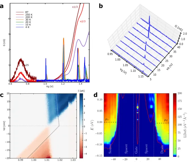
The linear S-D conductance of this device is plotted in Figure 1.2a at various temperatures between 4.2 K and 300 K. Here five resonances can be identified at 𝑉𝑔,𝑖≈ 0.7 V, 1.0 V, 1.2 V, 1.37 V and 1.45 V (𝑖 = 1−5).
The effect of the back gate (see figure 1.2b) is qualitatively simple: the resonances are simply shifted in gate voltage as the substrate bias is varied but they are not suppressed. A modulation of the amplitude of 𝐼𝑑𝑠 is also observed, which can be due to the ionization of a coupled impurity [46]. Yet, lines of finite conductance in the 𝐼𝑑𝑠versus (𝑉𝑔, 𝑉𝑏) plot are characteristic of the transport through a single AA, and not of two dots in series (which would lead to discrete triple points or more complicate patterns). Furthermore the AA resonances in the 𝑛-type sample have a large 𝛼𝑔= 0.75 (determined from the 𝐼𝑑𝑠(𝑉𝑔,𝑉𝑑) plot in figure 1.2c). Therefore, we conclude that this AA is below or very near the top gate, as in figure 1.1c.
The first resonance at 𝑉𝑔,1= 0.7 V carries a small resonant current at 300 K and no more detectable current below 𝑇 = 200 K. Thus, this first electron state is weakly tunnel coupled to the source and to the drain. At room temperature thermal activation of carriers increases the transmission through the nanowire under the spacers, which remains compatible with Coulomb blockade as shown in Ref. [37]. The resonances at larger 𝑉𝑔become increasingly
Vg [V] Vd [mV] I [pA] RT 250 K 200 K 30 K 20 K 10 K 4 K x25 x2/3
c
d
Figure 1.2 Conductance characteristics and Coulomb oscillations for a 𝑛-type
sam-ple a) Temperature dependence of 𝐺(𝑉𝑔) = 𝛿𝐼𝑑𝑠
𝛿𝑉𝑑 at 𝑉𝑏= 40 V. A first resonance appears at 300 K near 𝑉𝑔 = 0.7 V. Only four resonances are identified at 𝑇 = 4.2 K in this 𝑉𝑔 range. b)𝐼𝑑𝑠(𝑉𝑔,𝑉𝑏) at 𝑇 = 4.2 K around the second resonance. No triple point – as in figure 1.4 – but a single line appears in the 𝐼𝑑𝑠(𝑉𝑔,𝑉𝑏) plot, which is indicative of a single dot. c) 𝐼𝑑𝑠(𝑉𝑔,𝑉𝑑) at 𝑇 = 4.2 K around the second resonance. The first excited state (dashed-dotted line) appears 5 meV above the ground state for the resonance near 𝑉𝑔= 1 V. The lever arm parameter is 𝛼𝑔= 0.75. The large 𝛼𝑔confirms that the AA is centered under the top gate. d) Simulation of the confinement potential and Local Density of States (LDoS) in a 𝑛-type sam-ple with a ∼ 4 nm long dot (the AA) under the gate. The red line is the potential landscape in the channel, while the horizontal, black dashed lines are the Fermi levels in the source (𝜇𝑠) and drain (𝜇𝑑). Three quasiparticle states can be resolved in the dot under the gate.
sharper as the temperature decreases. The peaks at 𝑉𝑔= 1.0 V, 1.2 V, and 1.37 V have similar width at different temperatures but the value of the conductance 𝐺𝑟𝑒𝑠𝑖 at resonance as well as
its temperature dependence varies from peak to peak. Below 𝑇 = 30 K, 𝐺𝑟𝑒𝑠𝑖 is given by: 𝐺𝑟𝑒𝑠(𝑉
𝑔) ≈ 𝑒 2
4𝑘𝐵𝑇ΓΓ𝑠𝑠+ΓΓ𝑑𝑑, (1.1)
where Γ𝑠(𝑑)is the tunneling rate to the source (drain), and the full width at half maximum of the resonance is given by 3.52𝑘𝐵𝑇
𝑒𝛼𝑔, which is characteristic of a thermally broadened resonant tunneling regime.
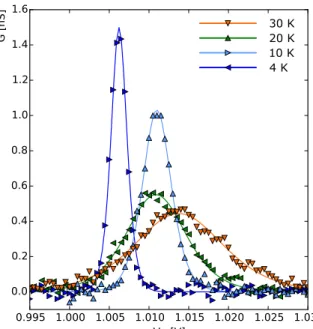
The resonance near 𝑉𝑔,2 = 1.0 V can be well fitted by a thermally broadened resonant tunneling lineshape (see figure 1.3):
𝐺2(𝑉𝑔) ≈ 𝑒4𝑘2
𝐵𝑇
Γ𝑠,2Γ𝑑,2
Γ𝑠,2+Γ𝑑,2cosh−2(𝛼𝑔𝑒(𝑉2𝑘𝑔𝐵−𝑉𝑇 𝑔,2)) (1.2) The full width at half maximum (FWHM) is hence set by the effective electronic temperature whatever the tunneling rates Γ𝑠(𝑑),2 (FWHM ≈ 3.52𝑘𝐵𝑇
𝑒𝛼𝑔). The fitted electronic temperature is 5.8 K (resp. 10.4 K, 21.8 K, 32.6 K) at 𝑇 = 4.2 K (resp. 10 K, 20 K, 30 K). The shift of the peak with 𝑉𝑔(𝑒𝛼𝑔Δ𝑉𝑔≃ 𝑘𝐵𝑇) between 4.2 K and 30 K has been explained in Ref. [47] for spin-degenerate states (with different Γ𝑠,2 and Γ𝑑,2). The resonant conductance 𝐺𝑟𝑒𝑠
2 is
consistent with Γ𝑠,2≃ 18MHz ≪ Γ𝑑,2.
For 𝑖 ≥ 3 the temperature dependence of 𝐺𝑟𝑒𝑠
𝑖 is non-monotonic between 𝑇 = 4.2 K and
𝑇 = 30 K, pointing out the contribution of a nearby, thermally accessible excited state to the resonant conductance, or to the temperature dependence of the tunneling rates. At higher temperature (200 K-300 K) a quasi continuum of states becomes accessible and contributes to the drain current at large V𝑔. Equivalently the tunnel rates strongly increase with tem-perature. This is not the case for the resonances near 𝑉𝑔,2 = 1.0 V and 𝑉𝑔,3= 1.2 V, so that the conductance is larger by several orders of magnitude at 4.2 K than at 300 K for these peaks. The addition energy of the one-to-two (resp. two-to-three, three-to-four, four-to-five) electrons in the channel is 230 (resp. 150, 130, 60) meV taking into account the lever arm parameter 𝛼𝑔= 0.75.
Simulations confirm this scenario. Figure 1.2d shows the local density of states (LDoS) computed in the 𝑛-type device of figure 1.1c, near the gate voltage where the first electron tunnels into the dot. The calculation was performed for 𝑇 = 150 K because at lower temper-atures some of the resonances become too narrow to be accurately resolved by the NEGF solver. There is only one, 4 nm long and diameter dot located near the center of the chan-nel. The dot is isolated from the bulk source and drain by lateral confinement within the spacers and by the dielectric mismatch between the nanowire and the embedding oxides (image charge self-energy corrections). Indeed both raise the conduction band of the wire
30 K 20 K 10 K 4 K
Figure 1.3 Temperature dependence of the resonance near 𝑉𝑔,2= 1.0 V in the 𝑛-type sam-ple. The symbols are the experimental points. The solid lines are the fits by the thermally broadened resonant tunneling theory (effective electron temperature as the fit parameter, see text).
well above the Fermi level of the contacts (the barrier is up to 300 meV high). Three well resolved energy levels can be identified inside the dot. The calculated addition energy for the second electron is 𝑈 = 196 meV. The dot is well coupled to the gate, the lever arm parameter 𝛼𝑔= 0.83 being close to the experimental one (0.75).
Simulations show that the orbital excitation in the channel always lie more than 15 meV above the ground state even in the absence of SR. Yet transport spectroscopy at finite 𝑉𝑑 reveals a single excited state at 𝑉𝑑 ≃ 5 meV as a plateau of current for both polarities (see figure 1.2c). The separation between the ground and the first excited state (5 meV) is there-fore much smaller than the calculated splitting between the orbital excitation. Consequently, the first excited state observed in figure 1.2c is most likely the valley orbit split ground orbital level in the AA. Indeed, the calculated valley-orbit splitting of the ground state resonance is strongly dependent on the shape of the dot and can range from a few to a few tens of meV.
In our samples a very good transmission through the 25 nm long spacers can be achieved for any temperature by adjusting the back gate voltage. The fact that the resonant current at 𝑇 = 4.2 K is comparable to the current measured at 300 K proves that any parasitic stochastic Coulomb blockade effect can be eliminated in our devices by a proper choice of the control voltages. In contrast to our results for the 𝑛-type sample, Shin et al. [48] have observed current resonances at room temperature which, however, split into multiple peaks at low
temperature. Furthermore, the current at the resonances decreases as the temperature is re-duced. The regular pattern of split peaks and their drain voltage dependence can be attributed (a) to the effect of valley splitting of orbital levels [30], (b) to a possible parasitic effect due to granularity in the gate stack [49] or (c) to the appearance of multiple dots in series.
1.2.2 Double dots device
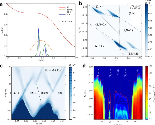
We present now a sample with a double-dot behaviour. In figure 1.4a we report the linear 𝐼𝑑𝑠− 𝑉𝑔 characteristics measured at various temperatures in a 𝑝-MOS device with a smal drain current. A broad resonance can be resolved at 300 K, and splits in two sharp resonances at 𝑇 = 4.2 K. In figure 1.4a, the back gate voltage 𝑉𝑏 has been adjusted in order to recover a high resonant current at low temperature – otherwise the current decreases by orders of magnitude between 𝑇 = 77 K and 𝑇 = 4.2 K. Such a decrease of the current is also visible in Ref. [30] and Ref. [43], where no back gate bias was applied. The splitting of the resonance and decrease of the current suggest the presence of two dots in series. The detuning (level misalignment) between the two dots results in a suppression of current at low temperature, unless the levels are properly realigned by the back gate electric field. This hypothesis is confirmed by the 𝐼𝑑𝑠(𝑉𝑔,𝑉𝑏) plot on figure 1.4b, where the current appears in a sequence of coupled triple points. The charging energy 𝑈 of these dots and lever arm parameter to the gate 𝛼𝑔= 𝛿𝑉𝛿Φ
𝑔 (Φ being the potential in the dot) can be determined from the 𝐼𝑑𝑠(𝑉𝑔,𝑉𝑑) plots. The larger is 𝛼𝑔, the stronger is the electrostatic coupling between the dot and the top Ω-gate. One of the dots has a charging energy 𝑈 ≃ 60 meV and a lever arm parameter 𝛼𝑔≃ 0.47. This dot is presumably located near the top gate [34, 35]. The other dot – the AA – has a larger charging energy 𝑈 ≃ 140 meV and a smaller 𝛼𝑔,AA≃ 0.34. It is likely located under a spacer and is induced by enhanced surface roughness.
In order to validate this scenario, we have calculated the charging energies and lever arm parameters of quantum dots with different sizes and positions along the nanowire. Figure 1.4d shows the LDoS computed in the device of figure 1.1d, which is the only geometry found that reproduces the overall experimental picture. In this device, we have introduced two constrictions under the source spacer that delimit a 4 nm diameter and 7 nm long dot (the AA), while a much longer dot extends from the gate to the drain spacer. The position and size of this 7 nm dot have been chosen to match the experimental charging energy and lever arm parameter of the AA. The other long dot results from random, gaussian surface roughness with rms Δ = 0.25 nm. Its charging energy is 𝑈 ≃ 45 meV, and its lever arm parameter is greater than 0.6, which suggests that the experimental accumulation dot is a little shorter on the gate side. There is one well defined resonance in the AA (the excited state being almost 50 meV below), and a few broader resonances in the long dot. The long
(1,N) (1,N+1) (2,N) (2,N+1) (2,N+2) (1,N+2) Vd = 3mV T = 300 mK RT 20 K 4 K 100 K Vd = 1 mV Ids [nA]
a
b
G [μS] (1,N) (1,N+1) (2,N+1) (2,N+2)c
Vb = -28.71Vd
Figure 1.4 𝐼𝑑𝑠(𝑉𝑔) characteristics and Coulomb oscillations for a 𝑝-type sample. a) Tem-perature dependence of 𝐼𝑑𝑠(𝑉𝑔) (𝑉𝑑= 1 mV). The resonance near 𝑉𝑔= −1.3 V at 𝑇 = 300 K splits in two resonances at 𝑇 = 4.2 K. The back gate voltage 𝑉𝑏= −30 V is adjusted in or-der to recover a high resonant current level at 𝑇 = 4.2 K. b) 𝐼𝑑𝑠(𝑉𝑔,𝑉𝑏) at 𝑇 = 4.2 K and 𝑉𝑑= 0.15 mV around the split resonance. The current appears at a series of coupled triple points that characterise double dots in series: One dot with a charging energy ≃ 60 meV is accumulated below the gate and modulates the current through the artificial atom (AA) under the spacers with a charging energy of ≃ 140 meV. At 𝑇 = 300 K the accumulation dot does not block the current and a single resonance due to the AA is observed (see text). c) 𝐺(𝑉𝑔,𝑉𝑑) at 𝑇 = 4.2 K along the dashed line of panel b. A charging energy of 60 meV can be deduced for the accumulation dot. The sawtooth pattern is due to the addition of one hole in the AA [46, 49]. d) Simulation of the confinement potential and Local Density of States (LDoS) in a 𝑝-type sample with a ∼ 4 nm long dot under the source spacer (the AA), and a ∼ 30 nm long dot under the gate and drain spacer. The red line is the potential landscape in the channel, while the horizontal, black dashed lines are the Fermi levels in the source (𝜇𝑠) and drain (𝜇𝑑). The resonances in the channel give the energy and spatial extension of the quasiparticle states. There is one well defined quasiparticle state in the AA.
I [nA]
(2, N+1)/(1, N+1)
(2, N+2)/(2, N+1)
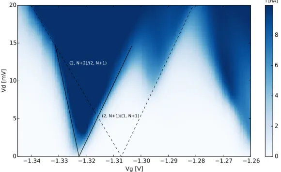
Figure 1.5 𝐼𝑑𝑠(𝑉𝑔,𝑉𝑑) at 𝑇 = 4.2 K for the 𝑝-type sample. The edges of the two cotunneling diamonds (see text) are marked with lines as guides for the eyes.
dot would typically contain around 4 − 5 holes (injected from the drain) when the ground state energy level in the AA comes in resonance with the source.
figure 1.5 shows the (𝑉𝑔,𝑉𝑑) stability diagram of figure 1.4c based on 𝐼𝑑𝑠 instead of 𝐺. The current flows only by cotunneling through the artificial atom at the (2,𝑁 + 2) → (2,𝑁 + 1) and (1,𝑁 + 1) → (1,𝑁) transitions. The lever arm parameter 𝛼𝑔≃ 0.47 of the quantum dot can be estimated from the shape of the main diamond. Another diamond is barely visible on figure 1.5. It is due to the cotunneling through the quantum dot at the (2,𝑁 +1) → (1,𝑁 +1) transition. The lever arm parameter 𝛼𝑔,AA≃ 0.34 of the AA has been estimated from this other diamond.
The addition energy for the 1h/2h transition is around 140 meV. It has been evaluated as the width of the 1 hole region (Δ𝑉𝑔≃ 400 mV, not shown) multiplied by the lever arm parameter 𝛼𝑔,AA.
1.3 Role of surface roughness
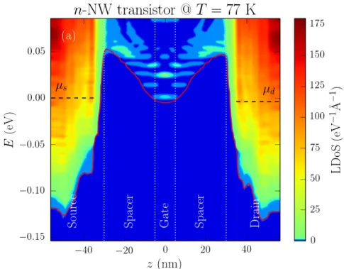
The local density of states (LDoS) in the conduction band of a smooth 𝑛-type device (Δ = 0) is plotted in figure 1.6a, at the gate voltage just before the first electron tunnels into the
nanowire. There is large, about 175 meV conduction band offset between the S/D and the entrance of the nanowire channel visible on the LDoS. This offset results from quantum confinement and exchange-correlation effects. As a consequence, the chemical potentials of the source and drain are around 50 meV below the conduction band edge of the nanowire, and a Schottky-like barrier appears between the highly-doped contacts and the insulating channel. The potential in the channel takes a near harmonic form whose depth is controlled by the gate; the first few quasiparticle states in this potential are clearly resolved on figure 1.6a as resonances in the LDoS of the channel.
Figure 1.6 LDoS in a smooth 𝑛-type sample. The red line is the potential landscape in the channel, while the horizontal, black dashed lines are the Fermi levels in the source (𝜇𝑠) and drain (𝜇𝑑). The resonances in the channel give the energy and spatial extension of the quasiparticle states of the nanowire. They are broadened by the coupling with the S/D and phonons. The calculations were performed at 𝑇 = 77 K. Note that the color scale is non linear at small LDoS, in order to emphasize the (small) LDoS in the channel with respect to the (very large) LDoS in the contacts
This is different from the simulation with larger surface roughness presented in figure 1.2d. In this case the SR disorder leads to formation of the dots in the potential and raises barriers between these dots (the top of the barrier is at 𝐸 = 97 meV on figure 1.6b). Although the potential remains deeper under the gate, the distribution of localized states is completely different from figure 1.6. The charging energy 𝑈12 tends to increase with disorder. It is
𝑈12≃ 65 meV in the smooth device of figure 1.6a and reaches 𝑈12≃ 90 meV in the rough device of figure 1.2d..
We can conclude from figure 1.6 that room temperature Coulomb blockade with addi-tion energies in the 200 meV range requires much stronger localizaaddi-tion along the nanowire. Etching and oxidation can indeed carve narrow constrictions along some nanowires (see fig-ure 1.4). Addition energies near 200 meV can be achieved in ∼ 4 nm long dots (with 4 nm diameter) separated from the rest of the channel by ≲ 2 nm diameter constrictions.
1.4 Conclusions
In summary, we have fabricated 3.4 nm diameter nanowire Ω-gate MOSFETs with deliber-ately long offset spacers (25 nm) and short gate length (10 nm) using DUV lithography and standard 300 mm CMOS process. Such a design isolates the channel from the source and the drain and enhances Coulomb interactions within the channel. As a result, these devices show robust addition spectra characteristic of artificial atoms. The shape and location of these artificial atoms depend on line edge roughness along the nanowire but the most promi-nent source of disorder, i.e. the presence of few cavities in series can be managed thanks to the control by both front and back gate voltages. The addition energy can reach up to 230 meV depending on the surface roughness. The orbital excited state is several 10 meV above the ground state and the measured valley orbit splitting is around 5 meV in 𝑛-type devices, a large value for a quantum dot [50]. These devices bridge conventional MOSFETS with SETs, and show that Coulomb interactions within the channel are bound to play an in-creasingly important role in the physics and design of the next generations of silicon devices. Finally, the on-chip integration of these artificial atoms with CMOS peripheral modules con-trolling their operation is very easy, since large size transistors are made with the very same CMOS technology [44].
Spin manipulation
In this chapter we investigate spin manipulation through spin resonance. We show a sample geometry tailored for this purpose and how mass-characterize it at room-temperature. We simulate the microwave behaviour of the on-chip antenna and how it can be used to drive spin resonance. Low temperature measurement are used to investigate spin blockade as a way for spin initialization and readout. We show signature of spin resonance and the effect of the valleys in the silicon conduction band. A theoretical model with numerical simulation is presented to explain the origin of the resonance signal. Selected measurement of a possible coherent spin manipulation (Rabi oscillation) are also presented.
2.1 Device
We want to study a system made by two coupled quantum dots in series. They should ex-hibit spin blockade for spin readout and show detectable transport down to the few-electron regime. To perform spin manipulation, we want a high frequency oscillating magnetic field applied to the spin confined in to the dots.
The dots are created on a 30nm-wide, 12nm-thick silicon nanowire, with two 35nm-long metallic gates over that. Spacing between the gates is about 30nm and this area is filled with 30nm wide spacers. These gates behaves as accumulation gates and create a dot underneath them. The NW section in-between is not gated and acts as tunnel barrier linking the two dots; the same is valid for the link between the dots and the leads (see section B and [51, 17, 52] for more details). In the latter case, the tunnel barrier has been shortened on purpose with a long annealing that diffused dopants from the leads; in this way the system is sensible to first-electron tunnel events.
In order to generate the oscillating magnetic field to drive the spin rotation we use a on-chip coplanar stripline antenna (see section 2.1.1). To accommodate the antenna close enough to
sample, the accumulation gates should be slightly redesigned. Both gates comes from one side of the nanowire and are cut on its edge. So instead of a “full” tri-gate cross section that embrace the nanowire on three sides (see figure A.2), the gates cover only one side and the top (see cross section in figure 2.2a). This new gate geometry is only partially self-aligned; this shortcoming is compensated by the large spacers that covers all the active area between the two gates. However, the electrostatic control is lowered and very sensible to the small variation of gate lithography (see section 2.1.2). On the other side, the RF antenna has been placed. Since it can be DC biased, it acts also as global side gate. Given the smaller elec-trostatic coupling compared to the accumulation gates, dots will likely be accumulated in the opposite corner. In figure 2.1 a 3D rendering and SEM image of the sample (without backend connections)
G1
G2
S
D
D
(a) 3D Rendering of the sample without spacers.
Dotted in red the approximate dot shape (b) SEM image of sample after S/D epitaxy.Spacers are visible
Figure 2.1 The sample
Si SiO2 SiN HfO2 TiN HDD Si Gate 1/2 Gate RF W tSi Sff
(a) Transverse cross section of the NW showing the gate geometry
50nm
(b) Longitudinal TEM cross section
2.1.1 RF antenna
The role of the antenna is to deliver a gigahertz oscillating magnetic field to the confined spin. We aim to target a bandwidth roughly from 8 to 20GHz. In traditional ESR, this role is fulfilled by a macroscopic microwave cavity. This cavity is designed in a way to have stationary modes and the samples is placed in a position where the magnetic field oscillation are maximum (antinode) and the electrical field is minimum (node). It’s crucial to minimize the radiated electrical field, because it heats the sample and leads to parasitic effects (such as photon assisted tunnelling) that can hide or suppress ESR signal.
Instead of a cavity we employed an on-chip coplanar stripline (CPS) [13]. In our case is ba-sically a side gate connected on both sides to pass a current (see the red object in figure 2.1a). The resulting wire is parallel to the silicon nanowire and the generated magnetic field (𝐵1) should be perpendicular to the substrate surface. If the static magnetic field (𝐵0) is applied “in-plane” (parallel to the surface), the two fields are always perpendicular: 𝐵0⟂ 𝐵1. The antenna is made from the same layer of accumulation gates and the lowermost layer is made by TiN, which is a superconductor (see 2.1.1).
To maximize magnetic field and minimize electric field, we want drive the stripline with an odd-transmission mode, where the voltage polarity on the sides of the stripline is opposed. The opposite is an even-mode transmission, where the ends oscillates together. The trans-mission line connecting the stripline is crucial to deliver such mode and not dissipate power to the environment. The device coupling a waveguide (like a coaxial cable) with a stripline is called balun; it couples an unbalanced line (waveguide) to a balanced line (stripline). A fully integrated balun has been studied in details in [53]. Our design is constrained by the backend design, which is done only for DC connections and cannot be tuned. To resolve this issue, we simulated the RF behaviour of the stripline and its connections to properly evaluate their performances.
In figure 2.3a we can see the mask level for the backend. In orange are drawn the “IN” and “OUT” bonding pads for the stripline. The stripline is connected to the backend through tungsten vias. In figure 2.3b we can see a TEM cross section showing the two copper metal levels (identical on the mask), the copper vias connecting them and the tungsten via. Below the backend lines there is a metallic plane, which is a leftover of the gate level after the EBL lithography (green in the image). It effectively acts as a ground plane (GP) for the transmission lines, thus we talk about microstrip transmission lines, even if it’s not assured that they are 50Ω matched. To properly ground this ground plane we bonded all the pads near the sample. These pads were made for devices with other purpose and not implemented in our fabrication process; these pads reach the GP with several tungsten vias. The
pre-metal dielectric (the dielectric that separate the device itself from the backend lines) is made by approximately 40nm of SiN and 260nm of SiO2, so the capacitance created by the pads
with the GP is not negligible: for 70x70μm pads it’s approximately equal to 0.64 pF. Given this big capacitance, we didn’t bond the “OUT” bond pad, since the ground return at high frequency is fully provided by the ground plane. Since the GP is bonded with several bond wires, the total impedance to the ground is low, contrarily to one single bond wire (see the lumped element model of the circuity in figure 2.3c). As positive side effect, the “OUT” pad behave as on-chip DC-block; the antenna is open on one side for the DC, so it can be easily used as side gate.
Another thing that has to be taken into account is the bonding wire length. As rule of thumb, one millimetre of bonding wire add 1 nH of inductance; due to constrains of the sample size, pad arrangement and the chip carrier, the length of our bonding wire is about 6mm, which leads to a non-negligible inductance of 6nH.
Superconductivity
As stated before, the titanium-nitride in the antenna is well-known superconductor [54]. This greatly helps to reduce as much as possible the self-heating due the microwave, since it re-duce the joule heating to the flow of current. TiN is a disordered superconductor with critical temperatures up to 4.5K [55]. Its properties are strongly dependent on the film thickness, which in our case is only 5nm. To characterize this film, we performed transport measure-ments on a straight wire with the same material stack and similar width (in centre, extension are larger to accommodate contact pads). The wire has been contacted twice on both side to perform 4-wire resistance measurements.
In figure 2.4a we can see the resistance as function of temperature and we clearly re-mark that we a have a superconducting transition around 1.3K. The Resistance before the transition (about 1050Ω, which gives a sheet resistance of RS= 18.1 Ω/2) is lower than the expected one for a so thin TiN film [54]; this is consistent with a metal stack above the thin film. The critical current is up to 0.5μA at low temperature (figure 2.4b). Up to 0.9T the film is still superconducting, with as critical current of about 0.3μA (figures 2.4c 2.4d). The multiple peaks that are visible at low magnetic field are due to wider cross sections of the wire that undergoes transition at higher current and can be ignored.
From these measurements we can estimate the kinetic inductance (LS), which is a critical parameter for our simulations. The normal state resistivity cannot be evaluated directly from our measurements because of the others materials in the stack, so it has been estimated from similar samples in literature to be ρXX= 17.5μΩm. The superconducting energy gap at zero
OUT
IN
(a) Drawing of bonding pads and transmission lines 500nm METAL1 METAL2 VIA1 CONTACT
(b) TEM Cross section of the transimission lines
0.6pFPad1 0.6pF PAD2 5nH Bonding wires Stripline IN Stripline IN RF IN GND ANTE NNA Stripline OUT
...
(c) Lumped elements diagram of the antenna circuitry
temperature, has been estimated from BCS theory Δ(0) = 1.764𝑘𝐵𝑇𝐶≈ 0.2meV [56] and from that the magnetic penetration depth 𝜆(0) = √ ℏ𝜌𝑥𝑥
𝜋𝜇0Δ(0) = 3.8μm [57]. Finally the kinetic inductance is given by 𝐿𝑆= 𝜇0𝜆2(0)
𝑑 = 3.2nH/2. This value is pretty high for our purposes,
but it’s normal given the thickness of the superconducting film. Thus at high frequency the current flow would probably divided between the superconductor and the metallic polysili-con, which has a sheet resistance of RP = 18.1Ω2
0.5 1.0 1.5 2.0 Temperature [K] 0 200 400 600 800 1000 Resistance [ ]
(a) Resistance at different temperatures
1.0 0.5 0.0 0.5 1.0 Current [ A] 0 500 1000 1500 2000 Differential Resistance [ ] 70 140 210 280 350 420 490 560 630 700 770 840
(b) Superconducting gap at different temp. (mK)
2.0 1.5 1.0 0.5 0.0 0.5 1.0 1.5 2.0 Current [ A] 0.0 0.2 0.4 0.6 0.8 Field [T] 0 500 1000 1500 2000 2500 3000 3500 4000 Differential Resistance [ ]
(c) Evolution of superconducting gap in field
2.0 1.5 1.0 0.5 0.0 0.5 1.0 1.5 2.0 Current [ A] 0 1000 2000 3000 4000 Differential Resistance [ ] 0.00 0.04 0.08 0.12 0.16 0.20 0.24 0.31 0.41 0.51 0.66
(d) Superconducting gap at different fields (T)
Figure 2.4 Measurements of superconductivity of RF line
Simulations
To evaluate the performance of the antenna, we simulated its microwave behaviour. The goal of these simulations was to show that the antenna can generate an oscillating magnetic field on the dots site and evaluate its magnitude. Moreover we evaluated the electrical field and
50nm 0.0 0.5 1.0 1.5 2.0 2.5 3.0 3.5 B [ μΤ ] 5 10 15 20 25 30 E [V/m] 1 2 3 4 5 6 7 J [A/m] 50nm
(a) Simulation of magnetic and electric fields in the sample
8 10 12 14 16 18 20 0.4 0.5 0.6 0.7 0.8 0.9 S11 S21 S22 140 120 100 80 60 40 20 0 Frequncy [GHz]
Voltage ratio Phase [deg]
Backend 8 10 12 14 16 18 20 0.993 0.994 0.995 0.996 0.997 0.998 0.999 1.5 2.0 2.5 3.0 3.5 Frequency [GHz]
Voltage ratio Phase [deg]
S11
Antenna
(b) S-Params for the backend section an the antenna. Plain lines are for the magnitude, dashed line are for the phase
the heat dissipated. We employed Sonnet [58] which is a planar electromagnetic simulation software. It can simulate the response of multi-port 2D structures at microwave frequencies. We used it to evaluate the S matrix of our system and the current density distribution. We simulated the antenna its backend connections and bonding pads as reported. The character-istic dimensions spans from the 80nm of the antenna width to the 70μm of the bonding pads; to evaluate behaviour on small features we need a fine meshing of the structure, which leads to enormous computations time and memory. Thus we divided the circuit in the backend part and the antenna part, evaluated separately with different meshing and accuracy. We calcu-lated the S matrix of both structures; for the antenna we expect a short-circuit behaviour, so a S11close to one (fully reflective). The backend on the contrary should be a good transmis-sion line, with small reflected power. In figure 2.5b we can see that the antenna is an almost perfect short, while the backend reflections are not negligible; however the transmission co-efficient S21is still reasonable. We can use these values to evaluate the effective voltage that
reaches the antenna; the ratio of the input voltage to the output voltage is given by
𝑉ratio= 1−𝑆𝑆21
22𝐴11
where 𝐴11 is the reflection coefficient from the antenna. In figure 2.6 we can see this ratio evaluated for the backend alone and the same, but coupled to a 50Ω port with 6nH inductance in series to simulate the bonding wire. The voltage ratio is severely reduced in the second case. To complete the picture of the signal attenuation, we measured the attenuation of the RF lines in the fridges. It’s approximately linear with the frequency (in GHz):
Attenuation = (−30.1−0.81⋅𝑓)dB
Putting everything together, we find that for a signal on the top of the cryostat of +10dBm at 10GHz, we deliver an oscillating voltage of roughly 1mV.
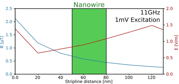
From this value, we can simulate the current density in the antenna and the electric field radiated. To calculate the magnetic field, we used the Biot-Savart law. For a current in a 2D plane we have 𝐁((𝑟)) = 𝜇4𝜋∫∫0 𝑆 𝐉(𝐫′)×(𝐫 −𝐫′) |𝐫 −𝐫′| d𝐬′= = 4𝜋𝜇0 ̂𝐤∫∫ 𝑆 𝐽𝑋(𝑥′,𝑦′)(𝑦−𝑦′)−𝐽𝑌(𝑥′,𝑦′)(𝑥−𝑥′) ((𝑥−𝑥′)2+(𝑦−𝑦′)2)3/2 d𝑥 ′d𝑦′
In figure 2.5a we can see the current density in the antenna and the distribution of the fields for a perfect odd mode. Around the antenna we get few micro-Tesla and Volts/meter. In figure 2.7 the fields are plotted for a cut perpendicular to antenna. We can see that the magnetic field on the nanowire is about 0.5μT, which can leads to a Rabi frequency (for g=2) CHECK
𝑓rabi= 𝑔𝜇ℎ = 14kHz𝑏𝐵1
The simulated heat flux generated by the antenna is about 40 μW.
Perspectives
Given the results of the simulations, our design can be improved in a next iteration. The antenna showed that a gigahertz magnetic field can be generated on-chip with a side gate. Titanium nitride is a good superconductor, with decent critical field and perfect compatibility with CMOS fabrication. However its limited thickness (5nm) harms both critical current and kinetic inductance, which limits the performance of the antenna in terms of thermal
8 10 12 14 16 18 20 Frequncy [GHz] 0.25 0.30 0.35 0.40 0.45 Voltage ratio Without bonding 60 50 40 30 Phase [deg] 8 10 12 14 16 18 20 Frequency [GHz] 0.02 0.04 0.06 0.08 0.10 0.12 Voltage ratio With 6nH of bonding 170 160 150 140 130 Phase [deg]
Figure 2.6 Simulations of the voltage attenuation for the copper backend without the bonding wire contribution (left) or with it (right). Plain lines are for the magnitude, dashed line are for the phase shift
0.0 20 40 60 80 100 120 Stripline distance [nm] 0.0 0.5 1.0 1.5 2.0 2.5 B [ μΤ ] 0.0 0.5 1.0 1.5 2.0 E [V/m]
Nanowire
11GHz
1mV Excitation
Figure 2.7 Simulations of generated fields (magnetic blue, electric red) as function of the distance from the stripline. In green is indicate the silicon nanowire
dissipation. One possible solution is to switch the gate technology to the so-called gate-last. In such case, the polysilicon layer is replaced by a metal, and that can be used to greatly increase the thickness of the superconductor. The layout of the antenna can be improved, by making a longer and wider wire instead of a sharp “U” shape. The backend connections should be tailored for microwave operations; 50-ohms port should be employed instead of simple DC-pads. A proper balun must be realized to propagate the correct differential modes and suppress the common ones. If permitted by the lithography, it should be done on the gate level instead of the metal level, in order to profit as much as possible of the presence of a superconductor. Another possibility is to use a full CPW design, with an antenna shorted at both sides as done in [59]. This design compared to CPS plus an integrated balun is much simpler to be implemented, since in the end it’s only a terminated CPW, which is relatively straightforward. However the generated magnetic field is only half of the CPS-based designs. Finally the sample holder should be designed with the sample in mind and minimize the length of the bonding wires, which is a major source of attenuation.
2.1.2 Selection
Samples with the required characteristic can be found in wafer 25 of batch “SiAM-2” (see table B.3). Twenty devices has been manufactured on this wafer and is essential to select the right one for the low temperature measurements. We performed a series of DC measurements at room temperature with the semi-automatic probe station and we employed a custom metric to rate the quality of the samples and infer some aspect of their low temperature behaviour. We took into account several criteria to compose the benchmark. First of all the mandatory “MOSFET” requirements:
• Undetectable gate leakage current for all the gates
• Threshold voltages must be reasonable; i.e. less than few volts • Sizable field effect for all gates; i.e. 𝐼𝑂𝑁/𝐼𝑂𝐹𝐹ratio
• Accumulation gates must be able to turn off the device; i.e. the 𝐼𝑂𝐹 𝐹 current should be small
• The 𝐼𝑂𝑁current should be sizeable
Then a a series of specific requirements specific to this geometry: • Accumulation gates should behave similarly
• Sub-threshold slope of accumulation gates is expected to be large (due to non-covering gates) but not excessive
• The side gate should have a moderate field effect and should be as effective as possible DIBL (Drain-Induced Barrier Lowering) and parameters linked to the behaviour of drain bias has not been taken into account.
We performed a series of six measurement for each device, as explained on the table 2.10. One gate has been swept, while the other have been kept in “Open” or “Closed” position. The voltages are specific of the gate stack materials and thickness.
The Set A (measurements OSC and SOC) tests the both of the accumulation gates when the RF gate is “closed”, so when it’s pushing the electrons against the opposite corner. The two traces tends to be very similar, because the corners of the accumulation gates are less susceptible to large variations. In Set B (measurements OSO and SOO) on the contrary the gate Rf is “open”, so it’s attracting the electrons on its side. In this case the traces differs, because the electrons are mostly accumulated below the whole accumulation gate and their extremities. These edges positions are more sensitive to variations in lithography, so it gives an hint about the real shape of the gate and how much is covering the nanowire. Finally the third Set C (measurements OOS and CCS) check the effectiveness of the RF gate. Since is relatively fare away from the sample (compared to the other gates), it can’t switch ON or OFF the conduction, but only modulating it when the other gates are “open”. When they are “closed” is expected to have no effect.
As an example, in figures 2.8a and 2.8b the plots of these measurements with the relative SEM image (2.8f) of a tested sample (sample (8,0)). From the photos we can see that Gate1 is partially covering the nanowire, while Gate2 goes a little beyond the nanowire edge. This is mirrored into the electrical measurements; while Set A measurements are indistinguishable, in the Set B they differs. The lower threshold and the higher sub-threshold slope for Gate1 compared to Gate2 is the consequence of their geometrical differences. By regrouping mea-surements of Set A and B by the swept gate (so meamea-surements OSC/OSO and SOC/SOO, figures 2.8c and 2.8c), we can see that the threshold voltages are shifted more by the RF gate when Gate1 is swept compared to Gate2. In fact Gate2 screen more the electric field of the RF gate than Gate1. Finally Set C (figure 2.8e) shows us more in detail how much the RF gate is effective in modulating the current. It’s pretty remarkable that tiny variations on the lithography greatly influence the transport behaviour even at room temperature.
On the contrary device (5,5) has similar gates, as can be seen in SEM image 2.9d. Its elec-trical characteristics (figures 2.9a and 2.9b) are thus much more regular and the gates work almost identically. From that we developed a series of parameters as benchmark:
3.0 2.5 2.0 1.5 1.0 0.5 0.0 0.5 1.0 1.5 Vg1 , Vg2 [V] 10-14 10-13 10-12 10-11 10-10 10-9 10-8 10-7 10-6 Idrain [A] Set A SOC OSC (a) Set A 3.0 2.5 2.0 1.5 1.0 0.5 0.0 0.5 1.0 1.5 Vg1 , Vg2 [V] 10-14 10-13 10-12 10-11 10-10 10-9 10-8 10-7 10-6 10-5 Idrain [A] Set B SOO OSO (b) Set B 3.0 2.5 2.0 1.5 1.0 0.5 0.0 0.5 1.0 1.5 Vg1 [V] 10-14 10-13 10-12 10-11 10-10 10-9 10-8 10-7 10-6 10-5 Idrain [A] Set A/B SOC SOO (c) Set A/B 3.0 2.5 2.0 1.5 1.0 0.5 0.0 0.5 1.0 1.5 Vg2 [V] 10-14 10-13 10-12 10-11 10-10 10-9 10-8 10-7 10-6 10-5 Idrain [A] Set B/A OSO OSC (d) Set B/A 3.0 2.5 2.0 1.5 1.0 0.5 0.0 0.5 1.0 1.5 VgRF [V] 0.2 0.0 0.2 0.4 0.6 0.8 1.0 1.2 Idrain [ μA] Set C OOS CCS (e) Set C 100nm (f) SEM Image
3.0 2.5 2.0 1.5 1.0 0.5 0.0 0.5 1.0 1.5 Vg1 , Vg2 [V] 10-14 10-13 10-12 10-11 10-10 10-9 10-8 10-7 10-6 Idrain [A] DEV 51 SOC OSC (a) Set A 3.0 2.5 2.0 1.5 1.0 0.5 0.0 0.5 1.0 1.5 Vg1 , Vg2 [V] 10-14 10-13 10-12 10-11 10-10 10-9 10-8 10-7 10-6 10-5 Idrain [A] DEV 51 SOO OSO (b) Set B 3.0 2.5 2.0 1.5 1.0 0.5 0.0 0.5 1.0 1.5 VgRF [V] 0.2 0.0 0.2 0.4 0.6 0.8 1.0 1.2 Idrain [A] 1e 6 DEV 51 OOS CCS (c) Set C 100nm (d) SEM Image
ION The current when a sweep reach the “open” value. Other gates could be either open or closed. It indicate if the device is conductive enough.
IOFF The current when a sweep reach the “close” value. Other gates could be either open or closed. It indicate if a gate has enough electrostatic control or not. If it’s elevate, it could mean that there are too much dopants into the channel to prevent depletion.
ION/IOFF The ratio of IONover IOFF. Especially useful for Set C to evaluate the coupling of a gate
VTH The threshold voltage. Formally defined as the voltage where strong inversion occurs [60] we calculated it with the Linear Extrapolation (LE) method [61, 62]. It give an indication where first-electron tunnel events will take place at low temperature. In order to have similar shaped and similarly lead coupling of dots, we look for similar value within the same Set (A and/or B)
SS The sub-threshold slope is inversely proportional to capacitive coupling of gate with
the electron gas. In this specific device their values are much higher than the mini-mum theoretical value at room temperature (60 mV/dec) due to shape of gates. Val-ues higher than the mean indicates either a bad coupling or an higher concentration of dopants below the gate. Similarly to the threshold voltage we look for similar values in the same Set.
Ig Gate leakage current. A current that flows from one gate to channel through the oxide. Must be the minimum possible.
IntD Integral difference. Is the difference of the logarithm of the area under two I(Vg)
curves in a Set: IntD = ∫log(𝐼(1)(𝑉𝐺)/𝐼0)−log(𝐼(2)(𝑉𝐺)/𝐼0)𝑑𝑉𝐺. Is another way to define the “symmetry” of two gates.
From these parameters and the comparison with samples that have been imaged, we can infer an approximation of the shape of the sample without SEM images.
In table 2.10 there are all these parameters for all the devices. In green is highlighted the best one according to our requirements that has been measured.
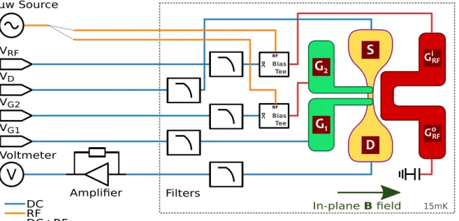
2.2 Setup and device connection
The sample has been pre-characterized at room temperature in the automatic probe-station as explained in sections 2.1.2 and B.1. Then, the selected sample has been put in a dilu-tion refrigerator, with a base temperature of 15mK. Gates and leads are connected up to
GATE 1 2 RF S E T A O S C O Open 1.5V S O C C Closed -3.0V B O S O S Sweep -3 ⇒1.5 V S O O C O O S C C S
Figure 2.10 Set of measurements performed at the probe station
Die V Threshold [V] Sub-threshold slope [mV/dec.] Ileak [fA]
SOC OSC SOO OSO SOC OSC SOO OSO G2 OOC G2 OOO G4 OOC G4 OOO
(0,7) 0.86 0.96 0.13 0.11 329 329 249 189 0 50 40 30 (-5,5) 1.04 -3.01 -0.70 -1.57 18 >999 5 297 >999 >999 >999 >999 (5,5) 0.59 0.61 0.10 -0.05 128 156 298 236 120 -550 -10 50 (0,4) 1.12 0.97 -0.38 0.05 274 289 417 179 410 -80 170 -40 (-7,3) 0.86 0.83 -0.48 0.05 210 190 317 269 100 -10 90 -120 (8,3) 1.10 1.21 0.04 0.09 330 336 251 254 60 30 10 50 (-4,2) 0.70 0.49 0.13 -0.01 154 126 154 166 -50 -10 120 120 (0,2) 1.23 0.84 -0.11 0.57 487 564 276 >999 100 100 0 150 (4,2) 1.09 -0.62 0.73 -0.45 320 286 >999 >999 -10 -120 -290 -70 (-8,0) 0.69 0.73 0.08 0.01 163 245 289 178 -20 -30 110 30 (0,0) 0.91 1.04 -0.22 0.14 272 244 334 154 -130 240 200 0 (8,0) 1.07 1.04 -0.09 0.16 243 233 385 151 770 -120 -40 -30 (-4,-2) 0.79 0.79 0.07 0.11 289 328 235 236 20 -120 30 -120 (4,-2) 0.72 0.64 -0.09 0.14 170 128 169 142 840 170 90 20 (-7,-3) 0.80 0.74 -0.43 -0.21 357 404 356 349 70 -150 150 40 (0,-3) 0.73 0.69 -0.04 0.14 182 161 234 170 90 10 70 150 (8,-3) 0.57 0.66 0.15 0.24 132 142 274 127 20 -380 30 -40 (-5,-5) 1.31 1.22 -0.60 0.04 273 305 310 195 120 -10 400 0 (0,-5) 1.28 1.31 -0.31 0.11 524 1142 312 254 220 100 -20 70 (5,-5) 0.80 1.01 -0.05 -0.12 137 200 343 332 -90 90 70 0
Die Distances IntD[V] IO N/IOFF
G1/G2 G1/RF G2/RF SOC/OSC SOO/OSO SOC/SOO OSO/OSC OOC OOO OOO/OOC COC OCC COO OCO
(0,7) 37.48 44.96 40.01 0.84 0.65 6.15 4.66 0.295 1.206 4.08 0 580 -20 840 (-5,5) 32.35 40.30 * 0.05 0.02 0.05 0.02 <0.001 <0.001 -0.75 20 20 20 -10 (5,5) 33.93 43.69 40.99 0.19 0.14 5.64 5.59 0.551 1.044 1.90 -20 0 0 10 (0,4) 37.29 38.11 35.04 0.76 6.26 12.44 5.42 0.218 0.990 4.53 -60 50 -40 30 (-7,3) 0.34 6.70 13.05 6.01 0.399 1.254 3.14 0 0 100 0 (8,3) 0.07 0.35 7.75 7.33 0.215 1.047 4.87 -110 -30 -120 0 (-4,2) 1.18 1.04 4.27 4.13 0.597 1.165 1.95 10 30 0 -150 (0,2) 3.85 14.89 10.98 0.06 0.002 0.618 >100 0 100 -20 -70 (4,2) 1.69 4.21 5.11 2.59 <0.001 0.001 9.49 -10 -170 70 8110 (-8,0) 26.53 40.72 * 0.07 1.88 6.84 5.03 0.516 1.172 2.27 -80 -110 60 -60 (0,0) 40.82 42.29 37.03 0.68 4.22 9.00 5.46 0.321 1.128 3.52 -170 -20 150 -90 (8,0) 32.85 45.98 36.35 0.19 4.17 9.73 5.37 0.257 1.065 4.15 -10 -90 0 -120 (-4,-2) 0.46 0.21 5.65 4.98 0.457 1.013 2.21 -100 -30 -10 0 (4,-2) 0.06 1.66 5.75 4.03 0.382 0.860 2.25 -20 -140 -90 20 (-7,-3) 0.45 1.12 10.74 10.08 0.447 1.210 2.71 -70 -130 21840 9820 (0,-3) 0.04 2.51 6.82 4.35 0.464 1.099 2.37 -190 -70 20 -140 (8,-3) 0.38 2.53 5.43 3.27 0.527 1.182 2.24 0 -60 -40 -90 (-5,-5) 31.18 31.98 54.57 0.80 6.93 15.43 7.70 0.052 0.741 14.29 -190 -50 3760 -120 (0,-5) 31.48 40.85 36.01 2.13 4.41 15.22 12.94 <0.001 1.012 >100 170 -230 120 -10 (5,-5) 31.32 41.22 32.50 0.90 0.24 8.60 9.74 0.358 1.121 3.13 30 10 -150 -50
ION[μA] IOFF[fA]
Figure 2.11 Results of room-temperature measurements for all candidates. When available, geometrical distances are reported. Non-working samples are grayed out
room-temperature by twisted pairs DC lines. The lines are filtered, both a room tempera-ture (500Hz low pass filters) and at the base temperatempera-ture (80MHz low pass filters, made by an home-made RC filters and Mini-Circuits VLFX-80). In addition to the DC signal, two high frequency lines with a bandwidth up to 20GHz are connected to the gate 2 and the RF stripline. These lines are used apply rapid pulses and/or microwave signals on the gates (see section 2.5.2 2.7). To reduce the thermal load, the line have thermalization points in terms of thermally anchored attenuators at the 1K, still and mixing plates.
In order to both apply a high frequency signal and DC bias on gate, these different signal get mixed at the base temperature by a bias-tee. The DC-Block is low rise-time commercial one (Tektronik PSPL5501A), while the RF filter is home-made on the chip carrier by a 10kΩ SMD resistance plus a wire that acts as inductor (see figure 2.12).
The chip carrier is PCB, with miniaturized connectors for 2 RF port and 24 DC lines. The substrate is ceramic-based, with copper metallic lines gold-plated, in order to have the best performances at high frequency.
The cryostat is equipped with a 2D vector magnet, which has been used to apply a static magnetic field in the plane of the sample. The angles in the text are expressed relative to the nanowire (ie. zero degrees means field parallel to the wire). The magnet is composed by two superconducting coils, which can reach a maximum of 9T/3T depending on the direction. DC signal are generated by low-noise opto-isolated DACs. Readout is performed by a tran-simpedance amplifier with a gain of 109V/A; a commercial multimeter is used to digitize the amplified signal.
Microwave signal are generated by an analogue microwave generator (Anritsu MG3693C), while fast pulses are generated by an Arbitrary Waveform Generator (Tektronik AWG520). These signals can be applied to the gate Rf or gate 2 (see section 2.7.1) for more details).
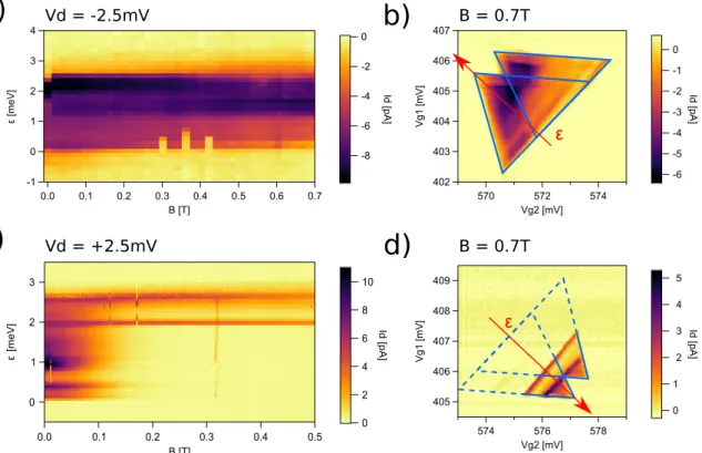
2.3 Stability diagram and bias spectroscopy
The selected sample has been cooled down to 15mK and the source-drain transport has been measured as function of all gates and drain bias voltage. The first goal was to drive the system in a mode where two dots in series are accumulated below the gates. We expect tunnel barriers to be formed in the access region below the outer spacers, as described in [35] The filling of these dots should be as low as possible and must exhibit spin-blockade (more on that 2.4). The signature of a double dot system is represented by a couple of conduction triangles in the plane of the gates voltages [63]. After the cooldown, we can compare the conductance measurements with the ones realized at room temperature (see figure 2.13). One gate has been kept on a high voltage (1V) to open its section of the channel, and the other one has been