HAL Id: hal-00669767
https://hal-iogs.archives-ouvertes.fr/hal-00669767
Submitted on 5 Apr 2012
HAL is a multi-disciplinary open access archive for the deposit and dissemination of sci-entific research documents, whether they are pub-lished or not. The documents may come from teaching and research institutions in France or abroad, or from public or private research centers.
L’archive ouverte pluridisciplinaire HAL, est destinée au dépôt et à la diffusion de documents scientifiques de niveau recherche, publiés ou non, émanant des établissements d’enseignement et de recherche français ou étrangers, des laboratoires publics ou privés.
A near-field actuated optical nanocavity
Benoit Cluzel, Loïc Lalouat, Philippe Velha, Emmanuel Picard, David
Peyrade, Jean-Claude Rodier, Thomas Charvolin, Philippe Lalanne,
Frédérique de Fornel, Emmanuel Hadji
To cite this version:
Benoit Cluzel, Loïc Lalouat, Philippe Velha, Emmanuel Picard, David Peyrade, et al.. A near-field actuated optical nanocavity. Optics Express, Optical Society of America - OSA Publishing, 2008, 16 (1), pp.279-286. �hal-00669767�
A near-field actuated optical nanocavity
Benoit Cluzel1,2, Loïc Lalouat2, Philippe Velha1,3,4, Emmanuel Picard1, David Peyrade4, Jean-Claude Rodier3, Thomas Charvolin1, Philippe Lalanne3, Frédérique de Fornel2 andEmmanuel Hadji1
1 Département de Recherche Fondamentale sur la Matière Condensée, Commissariat à l’Energie Atomique, 17 rue des Martyrs, F-38054 GRENOBLE Cedex 9, France.
2 Groupe d’Optique de Champ Proche, ICB, UMR 5209 CNRS , 9 av. Alain Savary, BP 47870, F-21078 DIJON Cedex, France.
3 Laboratoire Charles Fabry de l’Institut d’Optique, Centre National de la Recherche Scientifique, F-91403 ORSAY Cedex, France.
4
Laboratoire des Technologies de la Microélectronique, Centre National de la Recherche Scientifique, 38054 Grenoble, France.
benoit.cluzel@u-bourgogne.fr
Abstract: We demonstrate here that switching and tuning of a nanocavity
resonance can be achieved by approaching a sub-micrometer tip inside its evanescent near-field. The resonance energy is tuned over a wide spectral range (∆λ/λ~10-3) without significant deterioration of the cavity peak-transmittance and of the resonance linewidth. Such a result is achieved by taking benefits from a weak tip-cavity interaction regime in which the tip behaves as a pure optical path length modulator.
©2008 Optical Society of America
OCIS codes: (130.3120) Integrated optic devices; (250.5300) Photonic integrated circuits; (140.4780) Optical resonators; (999.9999) Photonic crystals;
References and links
1. S. I. Bozhevolnyi, V. S. Volkov, T. Sondergaard, A. Boltasseva, P. I. Borel, and M. Kristensen, “Near-field imaging of light propagation in photonic crystal waveguides: Explicit role of Bloch harmonics,” Phys. Rev. B. 66, 235204 (2002).
2. D. Gérard, et al., “Near-field probing of active photonic-crystal structures,” Opt. Lett. 27, 173-175 (2002). 3. H. Gersen, T. J. Karle, R.J.P. Engelen, W. Bogaerts, J. P. Korterik, N. F. van Hulst, T. F. Krauss, and L.
Kuipers, “Direct observation of Bloch Harmonics and Negative Phase velocity in Photonic crystal Waveguides,” Phys. Rev. Lett. 94, 123901-123904 (2005).
4. B. Cluzel, D. Gérard, E. Picard, T. Charvolin, V. Calvo, E. Hadji, and F. de Fornel, ”Experimental demonstration of Bloch mode parity change in photonic crystal waveguide,” App. Phys. Lett. 85, 2682-2684 (2004).
5. P.M. Adam, L. Salomon, F. de Fornel, and J. P. Goudonnet, “Determination of the spatial extension of the surface-plasmon evanescent field of a silver film with a photon scanning tunnelling microscope,” Phys. Rev. B 48, 2680-2683 (1993).
6. A. F.Koenderink, M. Kafesaki, B. C. Buchler, and V. Sandoghdar, “Controlling the Resonance of a Photonic Crystal Microcavity by a Near-Field Probe,” Phys. Rev. Lett. 95, 153904 (2005).
7. I. Märki, M. Salt, and H. P. Herzig, “Tuning the resonance of a photonic crystal microcavity with an AFM probe,” Opt. Express 14, 2969-2978 (2006).
8. I. Markï, M. Salt, F. Schädelin, P.-A. Künzi, U. Staufer, and H. P. Herzig, “Photonic crystal waveguides and tunable microcavities,” Proc. Optics in Computing, Topical Meeting (EOS), 19 (2004)
9. W.C.L. Hopman et al., “Nanomechanical tuning and imaging of a photonic crystal micro-cavity resonance,” Opt. Express 14 (19), 8745-8752 (2006)
10. J.T. Robinson, S. F. Preble and M. Lipson, “Imaging of highly confined modes in sub-micron scale silicon waveguides using Transmission based Near-Field Scanning Optical Microscopy,” Opt. Express 14 (22), 10588-10595 (2006).
11. C. Grillet, C. Monat, C.L. Smith, B.J. Eggleton, D.J. Moss, S. Frédérick, D. Dalacu, P.J. Poole, J. Lapointe, G. Aers, and R.L. Williams, “Nanowire coupling to photonic crystal nanocavities for single photon sources,” Opt. Express 15, 1267-1276 (2007)
12. B. Song, S. Noda, T. Asano and Y. Akahane, “Ultra-high-Q photonic double heterostructure nanocavity,” Nature Materials 4, 207-209 (2005).
#81095 - $15.00 USD Received 16 Mar 2007; revised 20 Jul 2007; accepted 1 Aug 2007; published 3 Jan 2008
13. Y. Tanaka, T. Asano, R. Hatsuta, S. Noda, “Investigation of point defect cavity formed in two dimensional photonic crystal slab with one sided dielectric cladding,” Appl. Phys. Lett. 88, 011112 (2006).
14. C. Sauvan, G. Lecamp, P. Lalanne, J. P. Hugonin,”Modal-reflectivity enhancement by geometry tuning in Photonic Crystal microcavities,” Opt. Express 13, 245-255 (2005).
15. P. Vehla, J. C. Rodier, P. Lalanne, J. P. Hugonin, D. Peyrade, E. Picard, T. Charvolin, and E. Hadji, “Ultra-high reflectivity photonic bandgap mirrors in a ridge SOI waveguide,”App. Phys Lett. 89, 171121 (2006) 16. Q. Xu, B. Schmidt, S. Pradhan, M. Lipson, M. “Micrometer-scale silicon electro-optic modulator,” Nature
435, 325-327 (2005)
17. E. Silberstein, Ph. Lalanne, J. P. Hugonin, Q. Cao, “On the use of grating theory in integrated optics,” J. Opt. Soc. Am. A. 18, 2865-75 (2001).
18. J. T. Robinson, C. Manolatou, L. Chen, and M. Lipson, “Ultrasmall Mode Volumes in Dielectric Optical Microcavities,” Phys. Rev. Lett. 95, 143901 (2005).
19. H. G. Craighead, “Nanoelectromechanical systems,” Science 290, 1532-1535 (2000).
20. M. L. Roukes, “Nanoelectromechanical systems face the future,” Phys. World 14, 25-31 (2001). 21. S. Mujumdar, F. Koenderink, R. West, V. Sandoghdar, “Nano-Optomechanical Characterization and
Manipulation of Photonic Crystals,” IEEE J. Sel. Top. Quantum Electron. 13, 253-261 (2007)
1. Introduction
So far near-field optics has been mostly devoted to the observation of light distribution inside optical nanodevices using Scanning Near-field Optical Microscopes [1-5] (SNOM). The probe generally consisting of a dielectric tip was not supposed to modify the observed system [5]. However, while optoelectronic devices are being miniaturized down to nanometer scale, the interaction between a sub-wavelength tip and a nanocavity is becoming increasingly important[6-9]. As a matter of fact, it has been recently predicted [6] numerically that the introduction in the cavity optical near-field of a high optical index tip should allow to tune the resonance of a photonic crystal microcavity. The very first trials to observe such an effect were obtained very recently but only at the expense of a strong cavity quality factor (Q) damping [7],[9] that could be attributed to the dramatic losses induced by the presence of the probe [10] near the cavity. These losses might be a severe limitation if applications such as on-chip information processing or strong light-matter interaction control by the way of a near-field probe are envisioned. Such applications would indeed require keeping the light strongly confined or localized within the chip, otherwise the information content or the light-matter interaction would vanish. This limitation has been successfully overcome very recently [11] by using a low index silica tapered fiber optical evanescently coupled to a photonic crystal nanocavity. However, compared to the SNOM techniques, the evanescent coupling techniques with fiber are non-local techniques since they do not rely on a sharp tip that can be accurately positioned by using a near-field scanning technique. In this work, we propose a system in which a lossless interaction regime between a SNOM silica tip and an ultra-low volume nanocavity is achieved, leading to a cavity resonance tuning without breaking the tight light confinement within the wave guided device.
We first designed and fabricated a high-Q ultra small-V nanocavities on SOI substrate and then we tuned their resonances, with almost no degradation of their optical properties, by introducing in the optical near field of the nanocavities a low index silica nanometric tip. Next, the interaction between the silica tip and the nanocavity is modeled and we show that such a reported tuning can be achieved as the tip operates in weak-interaction regime with the cavity and acts as a pure optical path-length modulator.
2. Nanocavity design and fabrication
In order to explore the near field optical interaction between a nanometric tip and a nanocavity, we designed and fabricated an ultra-small V high-Q nanocavity on silicon on insulator (SOI) substrate. Figure 1 shows different views, obtained by scanning electron microscopy, of the nanocavity. The nanocavities are composed of two mirrors made of sub-wavelength air holes etched into a SOI ridge waveguide supporting a single transverse-electric (TE) polarized guided-mode. They offer a very small modal volume V of 0.6(λ/n)3 with a single resonance over the 400 nm wide mirror band-gap. While high Q factor were
#81095 - $15.00 USD Received 16 Mar 2007; revised 20 Jul 2007; accepted 1 Aug 2007; published 3 Jan 2008
demonstrated [12] for air-standing silicon membrane structures, it is by comparison much more difficult to reach high Q for PC standing on silicon on insulator (SOI) substrates [13] due to a lower field confinement of the wave guided mode. However this later configuration, on substrate, presents a great interest in terms of applications for its greater robustness. So, in order to achieve high-Q's on SOI substrates, the cavity design carefully takes into account the non-symmetry of the SiO2/Si/air layer stack. This design allow to tailor the radiation losses at the cavity-mirror interfaces by implementing a gradual variation of the transverse mode profiles, i.e. by tapering the defect-ridge guided mode into the associated mirror Bloch mode[14]. Each mirror is formed by a periodic row of N air holes with a 200 nm diameter and a 370 nm periodicity, and by a 4-hole taper with a gradual increase of diameters, from 135 to 200 nm, and of inter-hole distances, from 300 to 350 nm. As the number N of holes in the periodic section of the mirror increases, the mirror modal reflectivity and the cavity Q also increase: as N → ∞, the cavity Q is limited by out-of-plane radiation losses and for λ = 1.6 µm, the extrapolated value for the unloaded Q is larger than 40,000, the theoretical value being ten times larger [15]. Nanocavities with N = 2, 3 and 4 holes have been manufactured using electron-beam lithography followed by a plasma etching in a Silicon-On-Insulator substrate with a 0.38-µm-thick silicon film and a 2-µm-thick buried oxide layer. Hereafter, only the cavities with N = 3 and 4 holes will be considered. Their measured Q's are respectively equal to 2800 and 7200, in very good agreement with the theoretical values [15].
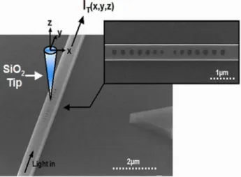
Fig. 1. Scanning Electron Micrograph views of the nanocavity. The cavity (N=3 in the picture) is formed by the association of two pairs of tapered mirrors etched in a 520-nm wide ridge waveguide. The cavity position is pointed by a triangle on the sample, allowing an optical pre-alignment between the tip and the microcavity. As superimposed schematically, in our experiments, we introduce a silica tip inside the optical near-field of the nanocavity and study the interaction between the tip and the light confined inside the resonator.
3. Nanocavity tuning experiments
In the following experiments, we use an end-fire setup to measure the cavity transmission spectra. Light injection from a TE-polarized tuneable laser source and output light collection onto an InGaAs detector are performed by using microscope objectives and monomode polarization-maintaining optical fibres. While accurately keeping these alignments, a ≈250 nm diameter silica tip mounted on a SNOM is approached above the cavity defect as shown on Fig.1. Thanks to a shear-force feedback, the tip is maintained at a fixed distance (z = 4 nm) above the wafer. After recording topographical images of the cavity, the tip is positioned in the centre of the cavity by using piezoelectric scanners. We next recorded the cavity transmission spectra for two different configurations (Fig. 2(a)). For the first configuration (up), the tip is positioned well above the cavity and does not interact with the optical near-field of the cavity mode (z> 100). For the second configuration (down), the tip is located just
#81095 - $15.00 USD Received 16 Mar 2007; revised 20 Jul 2007; accepted 1 Aug 2007; published 3 Jan 2008
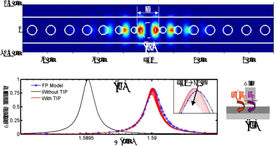
above the cavity (z = 4 nm). The recorded spectra exhibit a Lorentzian signature (bold curves in Fig. 2(b) and 2(c)) with superimposed high-frequency Fabry Perot fringes resulting from the bouncing of light between the cleaved facets of the wafer. The access ridge waveguides being about 10-mm-long, these oscillations are completely resolved by the 0.01 nm wavelength laser incremental shift used for recording the data.
As shown in Fig. 2(b) and 2(c), the presence of the tip strongly modifies the resonance of the cavities. It produces a red-shift of the resonance wavelength from λrup = 1585.6 nm to λrdown = 1586.4 nm on the Q = 2800 cavity. The red-shift value, 0.8 nm, corresponds to a relative shift of δλ/λr = 5.1.10-4. In the Q = 7200 cavity case, this experiment is unfortunately limited by our laser source tuning range that only allows us to observe the ascending side of the red-shifted resonance. However this indicates that the resonance red-shift is up to 0.6 nm. Such values are one order of magnitude higher than that recently obtained by electro-optical modulation of the silicon refractive index[16]. Remarkably and in contrast to the previous works in this field [7],[9], the peak-transmittances at resonance and the Q-factor of the cavities are nearly unaffected by the presence of the tip near the cavity. On another hand, this value is lower compared to that one obtained by using the evanescent coupling technique of [11] since the perturbative element used in our work (the SNOM tip) is largely smaller than the wire used in [11].
Fig. 2. Cavity tuning by a nanometric tip without Q-factor degradation. a) Schematic view of the experiment. b) and c) Transmission spectra recorded for two tip-cavity distances z, zup>100 nm (green curve) and zdown=4 nm (red curve) and for the Q=2800 and Q=7200 cavities.
The high-frequency oscillations are due to Fabry Perot fringes resulting from the bouncing of light between the wafer cleaved facets. Bold curves : lorentzian fits of the experimental spectra permitting to evaluate the Q-factor with an error bar of 10%. d) and e) Fabry Perot model predictions of the resonance peak red-shift for the two cavities. The model is described below. 4. Theoretical analysis of the cavity-tip interaction
In order to explain these effects, we have modeled the cavity-tip interaction. We first consider the cavity mode calculated with a 3D fully-vectorial aperiodic Fourier Modal Method (a-FMM) [17]. Figure 3(a) shows the dominant electric field-component Ex calculated at 4 nm above the ridge waveguide. Inside the cavity, this field exhibits a standing wave character with nodes and antinodes, which mainly results from light bouncing between the two mirrors. In Fig. 3(b), the solid black curve represents the spectrum of the cavity transmission Tcav calculated for N=4 and for a defect length D=435 nm. We have additionally calculated the
#81095 - $15.00 USD Received 16 Mar 2007; revised 20 Jul 2007; accepted 1 Aug 2007; published 3 Jan 2008
cavity transmission spectrum in the presence of a 300-nm tip for different on-axis locations xt of the tip inside the cavity defect. The calculation have been performed for 11 values of xt, varying from 0 to (D-d)/2≈70 nm, xt=0 corresponding to a tip located exactly in the cavity center. The results, shown by the red curves in Fig. 3(b), essentially show that the cavity transmission properties are almost independent on the actual on-axis tip location and that the presence of the tip only weakly affects the cavity Q (a maximum 10% decrease being inferred from the numerical data obtained for xt=70 nm).
0.5 µm 0
(a)
λ(µm)(b)
xt=0 1 µm 2 µm -2 µm -1 µm D xt=0 70 nm r=r1r2(c)
Tip T ran smi ssi o n - 0.5 µmFig. 3. Fully-vectorial analysis of the cavity tip interaction for a tip diameter d=300 nm. (a) Squared modulus of the dominant electric-field component |Ex|2 for the cavity mode, calculated
4 nm above the cavity. The mirror holes are superimposed for clarity reasons. A tip diameter of 300 nm is represented at the center of the cavity with a dashed contour. (b) Cavity transmission spectra (solid red curves) for a tip positioned above the cavity z=4 nm at 11 on-axis xt locations
from the center, by step of 6 nm. The solid black curve is obtained without tip. The blue circles are obtained with the Fabry Perot model, Eq. (1). The inset shows a zoom of the transmission T for the different positions. (c) Definition of the tip scattering coefficients, r1 and r2, on the front
and rear tip interfaces.
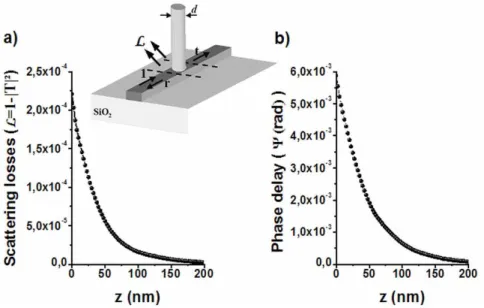
Although 3D-vectorial calculations performed for the entire tip-microcavity system allow for an accurate solution of the electromagnetic interaction in the vicinity of the device, they prevent a simple understanding. Indeed the photonic bandgap cavity behaves as a Fabry Perot resonator in which the fundamental ridge guided mode (effective index neff=2.7) is bouncing between the two mirrors. Instead of looking at a global property of the whole device, the basics of the cavity-tip interaction can thus be understood by considering the scattering of the bouncing mode by the tip, namely by considering the modal transmission t and reflection r coefficients of this mode, as shown by the inset in Fig. 4(a). Using the a-FMM, we have calculated these coefficients as a function of the tip-cavity distance z for different tip diameters, d = 250, 300 and 350 nm, in the range of the actual values used in the experiment. We found that |r(z)|2 is much smaller than 1-|t(z)|2 for any z. Thus, in this weak-backscattering interaction regime, 1-|t(z)|2 also represents out-of-plane radiation losses L resulting from radiation into the claddings and from scattering into the tip. Figures 4(a) and 4(b) show 1-|t(z)|2 and the normalized phase delay Ψ(z), defined by t(z) = |t(z)| exp(iΨ(z)), as a function of the tip-ridge distance. The most striking result is the smallness of the radiation losses; even for a 300 nm diameter tip located 4-nm above the ridge, the transmittance |t|2 is larger than 0.9997 (Fig. 4(a)).
The virtual absence of any back-reflection is an interesting property. The later holds for tip diameters that are approximately equal to a multiple of the standing-wave period, λ/(2neff) ≈ 300 nm, in the ridge. As illustrated in the inset of Fig. 3, for these specific
#81095 - $15.00 USD Received 16 Mar 2007; revised 20 Jul 2007; accepted 1 Aug 2007; published 3 Jan 2008
diameters, backscattering on the front (r1) and rear (r2) interfaces between the ridge and the tip section are almost exactly out of phase and cancel out. Using a Fabry Perot model and neglecting the tip-reflectance, the transmission Tcav of the cavity with a tip located at a distance z above the cavity is readily written as
(
0 effD)
2 M 2 2 M cav n ik 2 exp ) ²( t r 1 ) ( t T T z z − = (1)where rM is the mirror-modal reflectivity coefficient, TM is the mirror-modal transmittance and
D is the defect cavity length. The Fabry-Perot predictions of Eq. (1) are shown in Fig. 3(c)
with blue circles and well agree with the fully-vectorial electromagnetic results. The model shines real insight into the physics of the cavity-tip interaction. In contrast to the case of very small tips [6] (d<<λ/neff), it predicts that the interaction is independent of the axial location of the tip inside the microcavity; as long as the backscattered light remains smaller than the out-of-plane radiation losses L, |r|2 << L ≈1-|t|2, approaching the tip on a node or an antinode of the cavity mode results in identical effects. It also predicts that, for tip radiation losses smaller than the cavity losses, 1-|rM|2 < 1-|t|2, i.e. for cavity Q's smaller than 40,000, the tip behaves as a pure path-length modulator which modifies the effective cavity length without sacrificing the cavity Q-factor. Consequently, approaching the tip results only in a red-shift of the resonance wavelength ∆λ(z)/λ = Ψ(z)/[(1-rM²)Q] as evidenced experimentally (Figs. 2(b)-2(e)) and theoretically (Fig. 3(b)).
Fig. 4. Scattering by a cylindrical silica tip (n = 1.5) as a function of its distance z to a 520 nm wide, 340 nm high ridge waveguide for a tip having a 300 nm-diameter .(a) Scattering losses (L) and (b) Normalized phase delay (Ψ) under the tip approach in the vicinity of the silicon rib waveguide. The inset shows the definition of the tip scattering coefficients, r, t, and L for the fundamental mode of the ridge waveguide.
6. Actuated nanosystem demonstrator
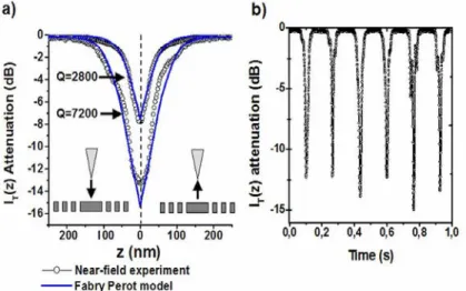
Finally, one can take benefits of this interaction to build a novel class of near field actuated nanosystems. For example, the tip-cavity nanosystem can obviously be considered as a nano-switch if we consider the transmittance of the cavity IT(z) for a given frequency while the tip-cavity distance z is modulated. Figure 5(a) shows the normalized transmission attenuation for λ = λrup, as a function the active parameter z. The tip is positioned above the cavity center in
#81095 - $15.00 USD Received 16 Mar 2007; revised 20 Jul 2007; accepted 1 Aug 2007; published 3 Jan 2008
the (x,y) plane and the z-axis is scanned for tip heights ranging from z =4 nm to z =250 nm while we record IT(z) at the same time. The measurements are performed for the two cavities. Two operation regimes may be distinguished. For z > 100 nm, the transmitted signal essentially remains constant. For z< 100 nm, the signal exponentially drops as the tip approaches the cavity surface. Such an exponential decay is characteristic of a near-field interaction process between the tip and the evanescent field of the cavity mode. Close to contact (z = 4 nm), the recorded attenuation reach 8dB (respectively 14dB) of the initial cavity peak transmittance (IMax) for the Q = 2800 cavity (respectively for the Q = 7200 cavity). As expected, the switching extinction ratio largely depends on the cavity Q-factor which is quantitatively predicted by the Fabry Perot model as illustrated by the blue curves in Fig.5a. From Eq. (1), the switching extinction ratio, defined by Tcav(z = 4 nm)/Tcav(z = 100 nm), is shown to be equal to [1+(Ψ0/πF)2], where F is the cavity Finesse and Ψ0 = Ψ(z = 4 nm).
Fig. 5. Switching operation of the cavity-tip nanosystem .a) Attenuation of the cavity transmittance (10.log(IT(z)/IMax)) as a function of the tip scan along the z-axis. The injected
wavelength is set to the resonance wavelength in absence of the tip (λrup) and the tip position in
the (x,y)-plane is set to the cavity center. As the tip approaches the surface of the cavity (z < 100 nm), the transmitted light decreases exponentially. Blue curves: model predictions according to Eq. (1). b) The transmittance attenuation measurement recorded while the tip height is modulated temporally (z(t)).
At last, the tip height above the cavity is modulated as a function of the time and the transmittance attenuation recorded is plotted on Fig. 5(b). It clearly shows the repeatability of the switching operation. We emphasize here that the time scale limited in our experiment to few Hz could reach the MHz range with the integration of other actuation systems directly nanofabricated on the SOI-chip, the switching time becoming only limited by the mechanical resonance[19].
8. Conclusion
In summary we have shown that a sub-µm dielectric tip, placed in the near field of a high-finesse photonic-bandgap microcavity, behaves as an optical path-length modulator. Such a system represents a basic building block toward the integration of on-chip optical switches or tunable filters. A very high level of integration could be achieved by replacing the SNOM tip by other actuation systems directly nanofabricated on the SOI-chip. A 14dB reversible switching operation together with a 0.8-nm-wide tuning have been observed, but better performances are anticipated by increasing the mirror reflectivity and by optimising the tip characteristics (size, refractive index..). Other cavity geometries relying on a high local field enhancement in air[18] and thus on a stronger tip interaction may also be used for further improvements. Even at this early stage of development, the present device may find use in a
#81095 - $15.00 USD Received 16 Mar 2007; revised 20 Jul 2007; accepted 1 Aug 2007; published 3 Jan 2008
broad range of applications. Since its tuning range is being compatible with WDM inter-channel wavelength spacing, it can be used for building electromechanical wavelength-division multiplexing routers, the time scale for switching being limited by mechanical resonance which could excess the MHz range with miniaturization [19]. For more fundamental science investigations, the device may also be used for finely matching the cavity-atom resonances in quantum electrodynamics experiments [11], or for enabling a direct detection and observation of nanoscale motions in NEMS [20], [21]. We believe that this kind of nanosystems may represent a new step towards Near-field Optics Nanometric Silicon Systems devoted to on-chip light manipulation at the nanometer scale.
Acknowledgements
The authors acknowledge the french Research National Agency for financial support in the context of the CHABIP and MIRAMAND projects.
#81095 - $15.00 USD Received 16 Mar 2007; revised 20 Jul 2007; accepted 1 Aug 2007; published 3 Jan 2008