Publisher’s version / Version de l'éditeur:
Optics Express, 18, 15, pp. 16146-16155, 2010-07-19
READ THESE TERMS AND CONDITIONS CAREFULLY BEFORE USING THIS WEBSITE. https://nrc-publications.canada.ca/eng/copyright
Vous avez des questions? Nous pouvons vous aider. Pour communiquer directement avec un auteur, consultez la première page de la revue dans laquelle son article a été publié afin de trouver ses coordonnées. Si vous n’arrivez pas à les repérer, communiquez avec nous à [email protected].
Questions? Contact the NRC Publications Archive team at
[email protected]. If you wish to email the authors directly, please see the first page of the publication for their contact information.
NRC Publications Archive
Archives des publications du CNRC
This publication could be one of several versions: author’s original, accepted manuscript or the publisher’s version. / La version de cette publication peut être l’une des suivantes : la version prépublication de l’auteur, la version acceptée du manuscrit ou la version de l’éditeur.
For the publisher’s version, please access the DOI link below./ Pour consulter la version de l’éditeur, utilisez le lien DOI ci-dessous.
https://doi.org/10.1364/OE.18.016146
Access and use of this website and the material on it are subject to the Terms and Conditions set forth at
Subwavelength grating crossings for silicon wire waveguides
Bock, Przemek J.; Cheben, Pavel; Schmid, Jens H.; Lapointe, Jean; Delâge,
André; Xu, Dan-Xia; Janz, Siegfried; Densmore, Adam; Hall, Trevor J.
https://publications-cnrc.canada.ca/fra/droits
L’accès à ce site Web et l’utilisation de son contenu sont assujettis aux conditions présentées dans le site LISEZ CES CONDITIONS ATTENTIVEMENT AVANT D’UTILISER CE SITE WEB.
NRC Publications Record / Notice d'Archives des publications de CNRC:
https://nrc-publications.canada.ca/eng/view/object/?id=4ce7e52d-df34-433c-8537-5b70b7121ecd https://publications-cnrc.canada.ca/fra/voir/objet/?id=4ce7e52d-df34-433c-8537-5b70b7121ecdSubwavelength grating crossings for silicon wire
waveguides
Przemek J. Bock1,2,*, Pavel Cheben1, Jens H. Schmid1, Jean Lapointe1, André Delâge1, Dan-Xia Xu1, Siegfried Janz1, Adam Densmore1 and Trevor J. Hall2
1Institute for Microstructural Sciences, National Research Council Canada, Ottawa, Canada 2Centre for Research in Photonics, University of Ottawa, Ottawa, Canada
Abstract: We report on the design, simulation and experimental demonstration of a new type of waveguide crossing based on subwavelength gratings in silicon waveguides. We used 3D finite-difference time-domain simulations to minimize loss, crosstalk and polarization dependence. Measurement of fabricated devices show that our waveguide crossings have a loss as low as −0.023 dB/crossing, polarization dependent loss of < 0.02 dB and crosstalk <-40 dB.
©2010 Optical Society of America
OCIS codes: (130.3120) Integrated optics devices; (050.1950) Diffraction gratings; (050.6624) Subwavelength structures.
References and links
1. P. Cheben, “Wavelength dispersive planar waveguide devices: echelle gratings and arrayed waveguide gratings,” in Optical waveguides: from theory to applied technologies, M. L. Calvo and V. Lakshminarayanan, eds. (CRC Press, 2007), 173–230.
2. C. R. Doerr, and K. Okamoto, “Advances in silica planar lightwave circuits,” J. Lightwave Technol. 24(12), 4763–4789 (2006).
3. X. J. M. Leijtens, B. Kuhlow, and M. K. Smit, “Arrayed waveguide gratings,” in Wavelength filters in fiber optics, H. Venghaus, (Springer Verlag, 2006), 125–187.
4. A. Densmore, M. Vachon, D.-X. Xu, S. Janz, R. Ma, Y.-H. Li, G. Lopinski, A. Delâge, J. Lapointe, C. C. Luebbert, Q. Y. Liu, P. Cheben, and J. H. Schmid, “Silicon photonic wire biosensor array for multiplexed real-time and label-free molecular detection,” Opt. Lett. 34(23), 3598–3600 (2009).
5. P. Cheben, J. H. Schmid, A. Delâge, A. Densmore, S. Janz, B. Lamontagne, J. Lapointe, E. Post, P. Waldron, and D.-X. Xu, “A high-resolution silicon-on-insulator arrayed waveguide grating microspectrometer with
sub-micrometer aperture waveguides,” Opt. Express 15(5), 299–306 (2007).
6. P. Cheben, J. H. Schmid, P. J. Bock, D.-X. Xu, S. Janz, A. Delâge, J. Lapointe, B. Lamontagne, A. Densmore, and T. Hall, “Sub-wavelength nanostructures for engineering the effective index of silicon-on-insulator waveguides,” 11th International Conference on Transparent Optical Networks, Azores, Portugal, June 28 - July 2, 2009, doi:10.1109/ICTON.2009.5185333.
7. A. Alduino, and M. Paniccia, “Interconnects: wiring electronics with light,” Nat. Photonics 1(3), 153–155 (2007). 8. H. Liu, H. Tam, P. K. A. Wai, and E. Pun, “Low-loss waveguide crossing using a multimode interference
structure,” Opt. Commun. 241(1-3), 99–104 (2004).
9. S. G. Johnson, C. Manolatou, S. Fan, P. R. Villeneuve, J. D. Joannopoulos, and H. A. Haus, “Elimination of cross talk in waveguide intersections,” Opt. Lett. 23(23), 1855–1857 (1998).
10. Y. Jiao, S. F. Mingaleev, M. Schillinger, D. A. B. Miller, S. Fan, and K. Busch, “Wannier basis design and optimization of a photonic crystal waveguide crossing,” IEEE Photon. Technol. Lett. 17(9), 1875–1877 (2005). 11. Y. Watanabe, Y. Sugimoto, N. Ikeda, N. Ozaki, A. Mizutani, Y. Takata, Y. Kitagawa, and K. Asakawa,
“Broadband waveguide intersection with low crosstalk in two-dimensional photonic crystal circuits by using topology optimization,” Opt. Express 14(20), 9502–9507 (2006).
12. W. Bogaerts, P. Dumon, D. Van Thourhout, and R. Baets, “Low-loss, low-cross-talk crossings for silicon-on-insulator nanophotonic waveguides,” Opt. Lett. 32(19), 2801–2803 (2007).
13. B. Luyssaert, P. Bienstman, P. Vandersteegen, P. Dumon, and R. Baets, “Efficient nonadiabatic planar waveguide tapers,” J. Lightwave Technol. 23(8), 2462–2468 (2005).
14. P. Sanchis, P. Villalba, F. Cuesta, A. Håkansson, A. Griol, J. V. Galán, A. Brimont, and J. Martí, “Highly efficient crossing structure for silicon-on-insulator waveguides,” Opt. Lett. 34(18), 2760–2762 (2009).
15. M. A. Popovic, E. P. Ippen, and F. X. Kärtner, “Low-loss bloch waves in open structures and highly compact, efficient Si waveguide-crossing arrays,” Proc. of 20th Annual Meeting of the IEEE Lasers and Electro-Optics Society, 56–57 (2007).
#127478 - $15.00 USD Received 23 Apr 2010; revised 15 Jun 2010; accepted 16 Jun 2010; published 15 Jul 2010
16. H. Kikuta, H. Toyota, and W. Yu, “Optical elements with subwavelength structured surfaces,” Opt. Rev. 10(2), 63–73 (2003).
17. C. F. R. Mateus, M. C. Y. Huang, L. Chen, C. J. Chang-Hasnain, and Y. Suzuki, “Broad-band mirror (1.12–1.62 m) using a subwavelength grating,” IEEE Photon. Technol. Lett. 16(7), 1676–1678 (2004).
18. P. Cheben, D.-X. Xu, S. Janz, and A. Densmore, “Subwavelength waveguide grating for mode conversion and light coupling in integrated optics,” Opt. Express 14(11), 4695–4702 (2006).
19. P. Cheben, S. Janz, D.-X. Xu, B. Lamontagne, A. Delâge, and S. Tanev, “Highly efficient broad-band waveguide grating coupler with a sub-wavelength grating mirror,”, in Frontiers in planar lightwave circuit technology, S. Janz et al., eds. (Springer, 2006), 235–243.
20. R. Halir, P. Cheben, S. Janz, D.-X. Xu, I. Molina-Fernández, and J. G. Wangüemert-Pérez, “Waveguide grating coupler with subwavelength microstructures,” Opt. Lett. 34(9), 1408–1410 (2009).
21. J. H. Schmid, P. Cheben, S. Janz, J. Lapointe, E. Post, and D.-X. Xu, “Gradient-index antireflective subwavelength structures for planar waveguide facets,” Opt. Lett. 32(13), 1794–1796 (2007).
22. J. H. Schmid, P. Cheben, S. Janz, J. Lapointe, E. Post, A. Delâge, A. Densmore, B. Lamontagne, P. Waldron and D.-X. Xu, “Subwavelength grating structures in silicon-on-insulator waveguides,” Adv. Opt. Technol. Special Issue on Silicon Photonics, (2008), Article ID 685489, doi:10.1155/2008/685489
23. P. J. Bock, P. Cheben, J. H. Schmid, A. Delâge, D.-X. Xu, S. Janz, and T. J. Hall, “Sub-wavelength grating mode transformers in silicon slab waveguides,” Opt. Express 17(21), 19120–19133 (2009).
24. P. J. Bock, P. Cheben, A. Delâge, J. H. Schmid, D.-X. Xu, S. Janz, and T. J. Hall, “Demultiplexer with blazed waveguide sidewall grating and sub-wavelength grating structure,” Opt. Express 16(22), 17616–17625 (2008). 25. S. M. Rytov, “Electromagnetic properties of a finely stratified medium,” Sov. Phys. JETP 2, 466–475 (1956). 26. P. Lalanne, and J.-P. Hugonin, “High-order effective-medium theory of subwavelength gratings in classical
mounting: application to volume holograms,” J. Opt. Soc. Am. A 15(7), 1843–1851 (1998).
1. Introduction
Extensive research into designing and fabricating complex waveguide devices for telecommunication applications [1–3] is now facilitating promising new applications in various areas, including sensing [4], spectroscopy [5,6] and interconnects [7]. Such devices benefit from the advantages of the silicon-on-insulator (SOI) material platform including compatibility with microelectronic fabrication and large scale integration. To fully exploit the potential of the SOI platform, these planar lightwave circuits (PLCs) require efficient waveguide crossings to facilitate connectivity and minimize device footprint.
Efficient waveguide crossings have been demonstrated in low index contrast glass waveguides ( n ~2%), for example by using the overlay between two multimode interference (MMIs) couplers [8]. Various waveguide crossings have also been proposed for high index contrast SOI waveguides. For example, photonic crystal waveguide crossings were originally proposed in [9], and have been optimized [10] and fabricated [11]. These structures exploit photonic crystal cavities to enhance coupling through the intersecting waveguide but suffer from high propagation loss and crosstalk. The resonant nature of these structures imposes stringent periodicity and small feature size requirements, consequently the performance of these crossings is largely susceptible to fabrication imperfections. Waveguide crossovers have also been proposed and fabricated using the overlap of parabolic MMIs [12]. Here, the combination of a shallow etch crossing region with deep etch tapered waveguides minimizes both loss and crosstalk, at the expense of added fabrication complexity. Using the principle of a nonadiabatic taper [13], a genetic algorithm was used to optimize a variable transverse width of a parabolic MMI, which can be fabricated with a single etch step [14]. Multiple waveguide crossings have also been theoretically investigated exploiting a narrow multimodal transverse field pattern with Bloch mode excitation from periodically spaced intersecting waveguides [15]. However, previous designs [13–15] are optimized for only transverse electric (TE) polarization and transverse magnetic (TM) performance is poor.
We propose subwavelength grating (SWG) waveguides for an efficient crossing with minimal loss, suppressed crosstalk and negligible polarization dependent loss (PDL). Subwavelength gratings have been used for years as a substitute for antireflective coatings on bulk optical surfaces [16]. Subwavelength gratings were also implemented as planar waveguide mirrors [17] and first proposed for high-index-contrast waveguides as efficient fiber-chip couplers [18]. Recently, SWGs have also been implemented as off-plane fiber couplers [19,20],
#127478 - $15.00 USD Received 23 Apr 2010; revised 15 Jun 2010; accepted 16 Jun 2010; published 15 Jul 2010
antireflective gradient index (GRIN) structures and interference mirrors [21,22], index matching structures at the slab-array boundary of an array waveguide grating (AWG) [23] and in a sidewall grating demultiplexer [24].
In this paper, we report on the design, simulation and experimental results of the first SWG waveguide crossing. Three-dimensional finite-difference time-domain (FDTD) simulation predicts low loss per crossing with minimal crosstalk and negligible PDL. The SWG crossings were fabricated using electron beam patterning and inductively coupled plasma reactive ion etching. Experimental characterization of our SWG crossings demonstrates low loss, with the additional advantages of negligible PDL and low crosstalk < −40 dB.
2. Subwavelength crossing principle
A waveguide intersecting another waveguide creates a region with no lateral mode confinement. Light propagating through the waveguide intersection diffracts causing loss due to excitation of radiation modes and crosstalk by coupling to the guided modes of the intersecting waveguide.
Our SWG design exploits the effective medium principle, which states that different optical materials, combined at subwavelength scales, can be approximated by an effective homogeneous material [25,26]. Within this approximation, an effective medium can be characterized by an effective refractive index defined by a power series of the homogenization parameter χ = Λ/λ, where Λ is the grating pitch and λ is the wavelength of light. Provided that the pitch Λ is less than the 1st order Bragg period ΛBragg = λ/(2neff), the grating is subwavelength and diffraction effects are frustrated. For the SOI waveguide platform, the two natural choices for the high and low index materials to create the effective medium are silicon (waveguide core) and silica (cladding) respectively. A gradual change in the ratio of Si to SiO2 along the light propagation direction (Fig. 1(a), z-axis) results in a corresponding effective refractive index change of the composite medium of the waveguide core.
We propose to use this effect to design a SWG mode converter for efficient waveguide crossings. This is done by gradually changing the effective index of the SWG waveguide through chirping the pitch and tapering the width of the grating segments (Fig. 1(a)). Reducing the segment width as the light propagates along the crossing expands the mode near the crossover point. Since the SWG waveguide intersecting this expanded mode is also subwavelength, diffraction is frustrated resulting in minimal loss. At the same time coupling to the intersecting waveguide is reduced. An important practical advantage of our design is that this crossover structure can be fabricated in a single etch step.
3. Subwavelength crossing simulation
We use 3D FDTD simulations with a mesh size of x × y × z = 10 × 20 × 10 nm3 to ensure finer resolution for the taper (x-coordinate, Fig. 1(a)) and chirp (z-coordinate, Fig. 1(a)). This increased numerical accuracy is at the expense of layout size, which is x × y × z = 3 × 3 × 10 m3 to maintain reasonable simulation time. Material refractive indices used are nSi = 3.476 and nSiO2 = 1.444 and the simulation time step is 1.67 × 10⁻¹⁷ s according to the Courant criterion t ≤ 1/(c(1/( x)2 + 1/( y)2 + 1/( z)2)½), where c is the speed of light in vacuum.
It should be noted the following limitation of our simulation procedure. From our previous theoretical and experimental results on SWG couplers [18,22] we identified an optimal coupler length of 50 m. Thereby, an optimal crossing geometry would require a total length of 100 m (two 50 m couplers). However, it is not possible to simulate a structure of this size using our 3D FDTD tool. To circumvent this limitation, we had to significantly reduce both the spatial resolution and the layout size, which also implies an increased numerical loss. Thereby, our numerical simulations should not be regarded as a rigorous procedure to obtain a fully optimized structure, but rather as a way to assess the relative influence of several structural parameters. The increased length of the fabricated SWG couplers, compared to the simulated structures, is expected to improve the taper loss, as it is demonstrated in section 4.
#127478 - $15.00 USD Received 23 Apr 2010; revised 15 Jun 2010; accepted 16 Jun 2010; published 15 Jul 2010
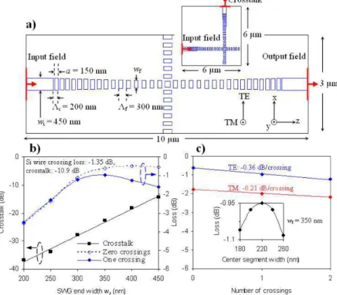
The simulation layout for a Si wire waveguide with a SWG crossing is shown in Fig. 1(a), where Λi and Λf are the initial and final grating pitches, wi and wf are the initial and final segment widths, a = 150 nm is the segment length and h = 260 nm is the Si thickness in the SOI wafer. This layout was used to calculate loss, whereas the layout inset in Fig. 1(a) was used to calculate crosstalk. A continuous wave (CW) fundamental mode of a 450 nm × 260 nm wire waveguide at λ = 1.55 µm is used as the input field and the simulation is performed for TE polarization. Mode mismatch loss is calculated as the power coupled to the fundamental mode of the output wire waveguide, whereas crosstalk is calculated as the power coupled to the fundamental mode of the intersecting waveguide.
To reduce the mode mismatch loss from a wire waveguide to SWG in Fig. 1(a), we ensure an adiabatic transition by a linear chirp (from Λi = 200 nm to Λf = 300) and taper (from wi = 450 nm to wf in the range of 200 nm – 350 nm) over 12 grating segments. The taper section is followed by 8 SWG segments with a constant pitch of 300 nm and a width of 300 nm (with a = 150 nm, i.e., a constant duty cycle of 50%). The intersecting SWG structure has the same grating parameters, while the center segment is square to ensure an identical geometry for both waveguides. For each wf, the center segment dimensions are set to match the area of the adjacent SWG grating segment (wf × a) ensuring a constant effective index for these adjacent segments. After the crossing point, an identical geometry is used for transition back to a wire waveguide (Fig. 1(a)).
Fig. 1. a) Top view of the 3D FDTD simulation layout for a Si wire waveguide with a SWG crossing, where Λi and Λf are the initial and final grating pitches, wi and wf are the initial and final segment widths and a = 150 nm is the segment length. Inset in (a) shows the layout for estimating crosstalk. b) Loss for zero SWG crossings (open diamond symbols), loss for one SWG crossing (full diamond) and crosstalk (square) for wf in the range of 200 nm to 350 nm for TE polarization at λ = 1.55 µm. Si wire crossing loss (−1.35 dB) and crosstalk (−10.9 dB) are indicated for reference. c) SWG loss per crossing for TE (blue) and TM (red) polarizations for wf = 350 nm. Inset in (c) shows loss for one SWG crossing with varying center square segment width w.
#127478 - $15.00 USD Received 23 Apr 2010; revised 15 Jun 2010; accepted 16 Jun 2010; published 15 Jul 2010
Figure 1(b) shows zero SWG crossings loss (SWG structure with no intersecting waveguide), and one SWG crossing loss and crosstalk calculated for various taper widths wf. As reference, calculated Si wire crossing loss is −1.35 dB, while crosstalk is −10.9 dB. Insertion loss for a SWG structure without an intersecting waveguide increases with narrower taper widths as the transition becomes less adiabatic. For a SWG structure with one intersecting waveguide, loss first decreases with narrower tapers (until wf = 350 nm) due to reduced crosstalk, then loss increases as the non-adiabatic taper loss dominates. Insertion loss is ultimately limited by a comparatively short 3 µm taper (12 SWG segments), which was chosen as a tradeoff with simulation time (20 hours). The loss penalty for adding a single crossing decreases significantly with narrower taper widths, and is as small as of −0.13 dB at a taper width of wf = 300 nm. For narrower taper widths, loss penalty is dominated by the large width change (wi to wf) over the 3 µm long taper. For a single crossing, crosstalk performance of −37 dB is calculated for a taper width of 200 nm, which is nearly a 30 dB improvement compared to a direct crossing of Si wires. At wider taper widths, coupling is increased to the intersecting waveguide mode, which deteriorates crosstalk as it is shown in Fig. 1(b).
To determine loss per SWG crossing, we use wf = 350 nm to minimize taper insertion loss (Fig. 1(b)). Loss per crossing is calculated as the slope of the linear fit to the insertion loss from three structures, comprising 0, 1 and 2 crossings. For two crossings to fit in the layout (Fig. 1(a)), the spacing between them was 4 grating segments. We used identical taper geometries for these three structures. Using this approach, the taper loss is factored out from the calculated loss per single crossing. Figure 1(c) shows that for TE polarization the loss is −0.36 dB/crossing, while for TM polarization the loss is −0.21 dB/crossing. This is a 1 dB loss decrease compared to the direct wire crossing loss of −1.35 dB for TE polarization (Fig. 1(b)).
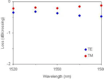
Fig. 2. Spectral dependence of simulated loss for a crossing structure with wf = 350 nm for TE (blue) and TM (red) polarizations for a wavelength range of 1520 nm – 1580 nm.
Wavelength dependence of the crossing structure was also calculated. Figure 2 shows the spectral dependence of simulated loss for a crossing structure with 350 nm tip width, with a loss variation of < 0.1 dB for TE and TM polarizations for a wavelength range of 1520 nm – 1580 nm.
The inset in Fig. 1(c) shows one SWG crossing loss (wf = 350 nm) for different widths of the center square segment indicating optimal performance at w = 220 nm. Such a square segment has the same area as the adjacent segments with dimensions a × w = 150 × 350 nm2, which is consistent with effective medium theory, i.e. no change in the effective medium for these SWG segments). Simulations predict a minimal (−0.05 dB) loss penalty for a center
#127478 - $15.00 USD Received 23 Apr 2010; revised 15 Jun 2010; accepted 16 Jun 2010; published 15 Jul 2010
square segment of w = 220 nm in a SWG waveguide with nominal segment dimensions a × w = 150 × 350 nm2.
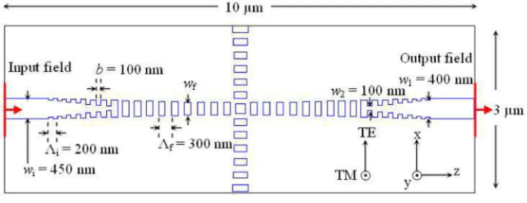
Fig. 3. Top view of the 3D FDTD simulation layout for a Si wire waveguide with a SWG crossing using bridging segments to reduce taper loss, where b = 100 is the bridging segment length and w1 = 400, w2 = 100 nm are the start and the end widths of the bridging segments.
To further refine the taper design and reduce insertion loss, we implemented bridging segments, as shown in Fig. 3. The bridging segments have constant length of b = 100 nm and their width varies from w1 = 400 to w2 = 100 nm. Using this technique, FDTD predicts taper back-to-back insertion loss is reduced from −0.61 dB (Fig. 1(b)) to −0.46 dB at wf = 350 nm for TE polarization at λ = 1.55 µm. Figure 1(b) indicates a compromise between optimizing SWG crossing loss and crosstalk, since the short non-adiabatic tapers dominate loss. To minimize loss due to non-adiabatic tapers, for fabrication we designed 50 µm long tapers with bridging segments as discussed in the next section. An important added advantage of using the bridging segments is the increased minimum gap size from 50 nm (Fig. 1(a)) to 100 nm (Fig. 3). While we used electron beam lithography to fabricate our structures, a minimum feature size of 100 nm is compatible with CMOS 193 nm optical lithography process.
4. Design and fabrication
Subwavelength grating crossing structures were implemented in a 6.1 mm long test chip. In our design, silicon wire waveguides (w = 450 nm) were transformed to the SWG straight waveguide using 50 µm long SWG taper with bridging segments (as in Fig. 3) followed by a 350 µm long SWG section with constant pitch, width and duty cycle. An identical taper was used for the transition back to a wire waveguide. To determine loss per crossing, we implemented crossing structures with 0, 1, 5, 10, 20, 40 and 80 crossings for two different SWG parameters sets A: Λi = 200 nm, Λf = 400 nm, wi = 450 nm, wf = 300 nm, ai = 150 nm, af = 200 nm and B: Λi = 200 nm, Λf = 300 nm wi = 450 nm, wf = 300 nm and ai = af = 150 nm. To estimate the SWG taper loss we concatenated 20, 40 and 60 tapers of design A. We also fabricated a set of Si wire waveguides with 0, 5, 20 and 40 crossings for a reference measurement.
We used commercially available SOI substrates with 0.26 µm thick silicon and 2 µm thick buried oxide (BOX) layers. Electron beam lithography was used to define the waveguide layout in high contrast hydrogen silsesquioxane resist, which formed SiO2 upon electron beam exposure. We used inductively coupled plasma reactive ion etching (ICP-RIE) to transfer the waveguide layout onto the silicon layer. Samples were coated with a 2 µm thick polymer (SU-8, n ~1.58 at λ = 1.55 µm), then cleaved into separate chips and facets polished.
Figure 4 shows scanning electron microscope (SEM) images of fabricated SWG crossings including multiple SWG crossings (Fig. 4(a)), one SWG crossing (Fig. 4(b)), detail of the crossing region (Fig. 4(c)) and SWG straight waveguide (Fig. 4(d)) prior to SU-8 coating. From the SEM images it was determined that a fabrication bias of 50 nm was present. Therefore the
#127478 - $15.00 USD Received 23 Apr 2010; revised 15 Jun 2010; accepted 16 Jun 2010; published 15 Jul 2010
actual dimensions of the SWG are Λ = 300 nm and w = 250 nm with a duty cycle of 33%. Actual wire waveguide width is 400 nm.
Fig. 4. Scanning electron microscope images of SWG crossings: a) multiple SWG crossings, b) one SWG crossing, c) detail of the crossing region with square center segment and d) SWG straight waveguide.
5. Experimental results
We used a polarization controller with a broadband (3 dB bandwidth of λ = 1530 nm - 1560 nm) amplified spontaneous emission (ASE) source to minimize Fabry-Pérot cavity effects from the chip facets. A tuneable external cavity semiconductor laser is used to measure the wavelength dependence of the crossings over a wavelength range λ = 1520 nm – 1580 nm. To couple the light into the chip, we used a lensed fibre resulting in a Gaussian beam waist of ~2 µm and a SWG fibre-chip coupler as described in [17]. Light is coupled out of the chip using another SWG coupler and subsequently focused by a microscope objective lens onto an InGaAs photodetector.
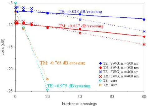
We estimated crossing loss by measuring SWG structures with 0, 1, 5, 10, 20, 40 and 80 crossings, where loss per crossing is determined as the slope of a linear fit of these measurements. Structures with varying number of waveguide crossings all have identical wire waveguide length, which eliminated the wire propagation loss from the loss-per-crossing measurement. Wire waveguide propagation loss was −3.1 dB/cm for TE and −3.2 dB/cm for TM polarizations for λ = 1.55 m, as measured on independent waveguide loss test structures. Figure 5 shows loss for SWG crossings (Λf = 400 nm and Λf = 300 nm) compared to direct wire waveguide crossings. For direct wire crossings, loss is −0.975 dB/crossing for TE and −0.763 dB/crossing for TM polarization. Using a SWG crossing with Λf = 400 nm, TE loss is reduced to −0.070 dB/crossing and TM loss to −0.067 dB/crossing, indicating a PDL of < 0.005 dB. Optimal performance was achieved for a SWG with Λf = 300 nm, where TE loss is −0.023 dB/crossing and TM loss is −0.037 dB/crossing (PDL < 0.02 dB). This is a 30 times loss reduction compared to direct wire crossing. An obvious improvement compared to FDTD
#127478 - $15.00 USD Received 23 Apr 2010; revised 15 Jun 2010; accepted 16 Jun 2010; published 15 Jul 2010
simulation predictions can be attributed to using longer tapers (50 µm instead of 3 µm) and the constrained layout size and resolution of the FDTD simulations.
The PDL at zero SWG crossings (TE = −6.9 dB, TM = −9.7 dB) compared to zero wire crossing (TE = −5 dB, TM = −7 dB) is attributed to the PDL of the fibre-chip coupler and the wire waveguide itself. The increased PDL for zero SWG crossings (0.8 dB) in Fig. 4(d) is the result of the PDL of the two extra SWG tapers used. We estimated SWG taper loss by measuring structures with 20, 40 and 60 concatenated 50 m long SWG tapers with bridging segments (as in Fig. 3) using the ASE source, where the taper loss is the slope of a linear fit of these measurements. The SWG taper had a measured TE loss of −0.296 dB and TM loss of −0.485 dB as shown in Fig. 6.
Fig. 5. Measured loss for SWG crossings with Λ = 300 nm for TE (blue diamond) and TM (red diamond) polarizations and Λ = 400 nm for TE (blue cross) and TM (red cross) polarizations using a broadband ASE source. Loss for direct wire crossings is shown for comparison for TE (green circle) and TM (cyan circle).
#127478 - $15.00 USD Received 23 Apr 2010; revised 15 Jun 2010; accepted 16 Jun 2010; published 15 Jul 2010
Fig. 6. Measured loss for a 50 µm long SWG taper with Λf = 400 nm and wf = 300 nm for TE (blue) and TM (red) polarizations using a broadband ASE source.
Fig. 7. Measured loss per crossing for a SWG crossings with Λ = 300 nm for TE (blue) and TM (red) polarizations using a tunable external cavity semiconductor laser.
Using a tunable external cavity semiconductor laser, the loss was measured for 10, 20, 40 and 80 crossings. Loss per crossing was estimated as the slope of the linear fit to these measurements for λ = 1520 nm – 1580 nm. Figure 7 shows the measured wavelength dependence of loss per crossing. The TE loss is −0.025 dB/crossing and TM loss is −0.045 dB/crossing at λ = 1545 nm, in accordance with the ASE measurements (ASE center wavelength of 1545 nm). Some ripple (~0.06 dB) in the TM loss per crossing is due to the increased TM reflection of the SWG couplers, which also results in an increased taper loss for TM polarization (Fig. 6), yielding a Fabry-Pérot cavity effect. The measured loss variation with wavelength is minimal, i.e. below 0.02 dB for TE and 0.06 dB for TM polarizations, in a wavelength range of 1520 nm – 1580 nm.
Crosstalk was estimated by coupling the light into a waveguide with a single SWG crossing and measuring the power from the output aperture of the intersecting waveguide. Crosstalk for both SWG crossings (Λf = 400 nm and Λf = 300 nm) was better than −40 dB, which is
#127478 - $15.00 USD Received 23 Apr 2010; revised 15 Jun 2010; accepted 16 Jun 2010; published 15 Jul 2010
approximately a 25 dB improvement compared to crosstalk measured for direct crossings of Si wire waveguides. Indeed, with narrower taper widths the mode delocalizes further and the crosstalk is expected to improve, as predicted by FDTD simulations in Fig. 1(b). However, there is a limit to expanding the mode size beyond the BOX thickness, which is 2 m in our SOI wafers, since this would result in a loss penalty due to light leakage to the substrate.
In terms of fabrication tolerances, the subwavelength nature of our structures results in a spatial refractive index averaging, such that the effects of fabrication imperfections are expected to be alleviated compared to resonant photonic structures such as photonic crystals. As we pointed out in the previous section, from the SEM images it was determined that a fabrication bias of 50 nm was present, yielding a deviations of 17% and 33% compared to designed values of segment width and length respectively. Notwithstanding this fabrication error, the structure still performs remarkably well, both in terms of crosstalk and loss (Fig. 5).
6. Conclusion
We have reported on a new waveguide crossing principle based on subwavelength grating waveguides, including the simulation, design and experimental demonstration. The measured loss of the fabricated structures is as low as −0.023 dB/crossing, polarization dependent loss is minimal (0.02 dB) and crosstalk is <-40 dB. An important advantage of our SWG structures is that they can be fabricated with a single etch step. Subwavelength grating crossings have the potential to facilitate massive interconnectivity and minimize the device footprint for future complex planar waveguide circuits.
#127478 - $15.00 USD Received 23 Apr 2010; revised 15 Jun 2010; accepted 16 Jun 2010; published 15 Jul 2010


![[PDF] Les services d’Asp.Net Ajax en pdf | Cours informatique](data:image/gif;base64,R0lGODlhAQABAIAAAP///wAAACH5BAEAAAAALAAAAAABAAEAAAICRAEAOw==)