HAL Id: hal-02145926
https://hal.archives-ouvertes.fr/hal-02145926
Submitted on 3 Jun 2019HAL is a multi-disciplinary open access
archive for the deposit and dissemination of sci-entific research documents, whether they are pub-lished or not. The documents may come from teaching and research institutions in France or abroad, or from public or private research centers.
L’archive ouverte pluridisciplinaire HAL, est destinée au dépôt et à la diffusion de documents scientifiques de niveau recherche, publiés ou non, émanant des établissements d’enseignement et de recherche français ou étrangers, des laboratoires publics ou privés.
Technological advances on Si and Si3N4 low-loss
waveguide platforms for nonlinear and quantum optics
applications
Cyril Bellegarde, Houssein El Dirani, Xavier Letartre, Camille Petit-Etienne,
Christelle Monat, Jean-Michel Hartmann, Corrado Sciancalepore, Erwine
Pargon
To cite this version:
Cyril Bellegarde, Houssein El Dirani, Xavier Letartre, Camille Petit-Etienne, Christelle Monat, et al.. Technological advances on Si and Si3N4 low-loss waveguide platforms for nonlinear and quantum optics applications. Proceedings of SPIE, the International Society for Optical Engineering, SPIE, The International Society for Optical Engineering, 2019, Advances in Photonics of Quantum Computing, Memory, and Communication XII, 1093309, pp.8. �10.1117/12.2508617�. �hal-02145926�
PROCEEDINGS OF SPIE
SPIEDigitalLibrary.org/conference-proceedings-of-spie
Technological advances on Si and
Si3N4 low-loss waveguide platforms
for nonlinear and quantum optics
applications
Cyril Bellegarde, Houssein El Dirani, Xavier Letartre,
Camille Petit-Etienne, Christelle Monat, et al.
Cyril Bellegarde, Houssein El Dirani, Xavier Letartre, Camille Petit-Etienne,
Christelle Monat, Jean-Michel Hartmann, Corrado Sciancalepore, Erwine
Pargon, "Technological advances on Si and Si3N4 low-loss waveguide
platforms for nonlinear and quantum optics applications," Proc. SPIE 10933,
Advances in Photonics of Quantum Computing, Memory, and Communication
XII, 1093309 (4 March 2019); doi: 10.1117/12.2508617
Event: SPIE OPTO, 2019, San Francisco, California, United States
Technological advances on Si and Si
3N
4low-losses waveguide platforms
for nonlinear and quantum optics applications
Cyril Bellegarde2, Houssein El Dirani1, Xavier Letartre3, Camille Petit-Etienne1, Christelle Monat3Jean-Michel Hartmann1, Corrado Sciancalepore1 and Erwine Pargon2
1Univ. Grenoble Alpes, CEA-LETI, Minatec, Optics and Photonics Division, 17 rue des Martyrs, F-38054 Grenoble, France 2 LTM, Centre National de la Recherche Scientifique, University Grenoble Alpes, 38000 Grenoble, France
3Institut des nanotechnologies de Lyon, UMR CNRS 5270, Ecole Centrale Lyon, Ecully, France
ABSTRACT
In this communication, we report on the design, fabrication, and testing of silicon-on-insulator (SOI) and silicon-nitride-on-insulator (SiNOI) photonic circuits for nonlinear and quantum optics applications. As recently demonstrated, the generation of correlated photons on Si platforms can be used for quantum cryptography and quantum computing. Concerning SiNOI waveguides, Kerr frequency combs have been proposed in many applications, such as atomic clocks, on-chip spectroscopy, and terabit coherent communications. Silicon is an attractive platforms for correlated photons sources because of its high nonlinearity, they can have several modes in telecom band with sharp line widths (tens of µeV) and its inherent complementary metal-oxide-semiconductor (CMOS) compatibility. Moreover, the SiNOI is an attractive platform for Kerr comb generation due to their large bandgap and consequently the low two-photon absorption in the telecommunication band. Furthermore, in all the previous SiNOI-based frequency combs, the silicon nitride film undergoes long and high-temperature annealing to reduce the absorption in the telecommunication band caused by the dangling N-H bonds, thus making such annealed Si3N4 films non-CMOS compatible. However, both in
the case of correlated photons pairs generation and Kerr frequency combs, the source efficiency is related to the quality factor (Q), so that a high-Q resonator is required to get highly-efficient sources. Authors report here about the fabrication and the characterization of annealing-free CMOS-compatible SiNOI- and hydrogen-annealed silicon-based waveguides and microresonators featuring ultra-low losses (e.g., 0.6 dB/cm for single-mode Si waveguides) that can be used, respectively, as efficient sources for Kerr combs and correlated photon pairs sources.
Keywords: Complementary metal-oxide-semiconductor (CMOS), nonlinear integrated optics, quantum integrated circuits,
Kerr-based comb generation, resonators, photonic integrated circuits (PICs), silicon nitride (Si3N4), correlated photons, hydrogen
annealing.
1. LOW-LOSS SILICON NITRIDE FOR NONLINEAR PHOTONICS
Kerr frequency combs constitute a paradigm shift in the development of high-capacity data transmission, integrated spectroscopy, high precision metrology, and frequency synthesis [1]. Since 2010, silicon-nitride-on-insulator (SiNOI) has imposed as an attractive chip-based platform for the generation of wideband frequency combs pumped at telecom wavelengths, because of its relatively high nonlinearity (×10 that of silica and larger than that of highly nonlinear Hydex glass [2]) as well as the absence of two-photon absorption and free carrier generation that plague crystalline silicon. In the meanwhile, silicon photonics integrated circuits (Si-PICs) have demonstrated increasing maturity levels for a wide range of optical functions such as III-V-on-Si integrated lasers [3], high-speed modulators [4], Ge-on-Si photodiodes [5], as well as filters and wavelength (de)multiplexers [6], thus continuously highlighting the potential of silicon optoelectronics integration with cost-effective complementary metal-oxide-semiconductor (CMOS) technology [7,8]. In this context, the monolithic co-integration of Kerr-based frequency combs with Si photonics holds the promise for on-chip high-capacity transmitters that would benefit from the maturity and low cost of CMOS manufacturing and scalability.
The realization of relatively thick (> 700 nm) stoichiometric Si3N4 films, as required by microring frequency combs, which imply both a tight confinement of light and anomalous group velocity dispersion (GVD), remains challenging. In
Advances in Photonics of Quantum Computing, Memory, and Communication XII, edited by Philip R. Hemmer, Alan L. Migdall, Zameer Ul Hasan, Proc. of SPIE Vol. 10933, 1093309
© 2019 SPIE · CCC code: 0277-786X/19/$18 · doi: 10.1117/12.2508617 Proc. of SPIE Vol. 10933 1093309-1
Downloaded From: https://www.spiedigitallibrary.org/conference-proceedings-of-spie on 10 May 2019 Terms of Use: https://www.spiedigitallibrary.org/terms-of-use
particular, all prior works strictly made use of long high-temperature annealing (~1200 °C for at least 3h) of the deposited silicon nitride film [9-12]. This extreme annealing step has been accounted for by the need to densify the silicon nitride film through driving out excess hydrogen and break N-H bonds, so as to get closer to a stoichiometric Si3N4 film and reduce the material absorption loss in the C-band. However, this annealing induces thermal stress that
eventually leads to cracks during the device processing unless sophisticated pre-patterning strategies are adopted prior to the film deposition [10, 11]. Yet, in the context of nonlinear optics-silicon optoelectronics co-integration, these extreme annealing temperatures would severely degrade the front-end silicon optoelectronics circuit underneath. Specifically, doped optical circuits would be unacceptably affected by the undesirable dopant diffusion in junction-based Si modulators and by the hetero-interface degradation of Ge-on-Si photodetectors. Very recently, we reported a new method that avoids thermal annealing for realizing relatively thick (740 nm) crack-free Si3N4-based straight
nanowaveguides with good linear and nonlinear properties measured by self-phase modulation [15].Here, we report for the first time the realization of annealing-free silicon nitride comb microresonators, following a tailored deposition method which minimizes the hydrogen content. Our annealing-free and crack-free fabrication process (shown in Fig. 1) provides our devices with the right specification (microring GVD and characteristics) to underpin Kerr frequency combs, thus representing a significant step toward the full compatibility of Si3N4-based Kerr comb sources with the
thermal budgets of Si photonics processing. In contrast to all previous approaches, our process does not exceed neither the dopant activation temperature (1030 °C) required for Si modulators [13], nor the H2 annealing thermal budget used
for dislocations control for Ge-on-Si photodiodes (825 °C) [14].
Fig. 1. Schematics of the annealing-free fabrication process for Si3N4 nonlinear photonics (a)-(f).
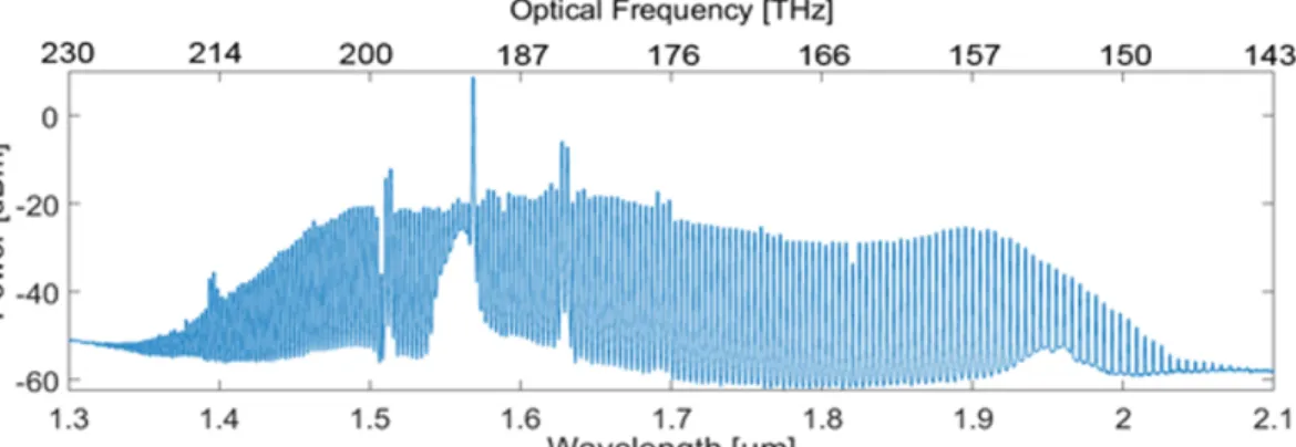
The measured spectrum of an annealing-free silicon-nitride-on-insulator microring with a 56-µm radius is shown in Fig. 2. A native line spacing frequency comb spanning across about 730 nm between 1340 nm - 2070 nm was measured when a continuous-wave pump power of ~ 1 W at 1569 nm– was coupled in the bus waveguide. The loaded quality factor of the ring resonator separated by a 350 nm gap from the bus waveguide exceeds 580,000 at the pump wavelength. The cross-section dimensions (1.5-µm-wide × 740-nm-thick) of the ring ensure that GVD is anomalous at the pump wavelength.
Proc. of SPIE Vol. 10933 1093309-2
Downloaded From: https://www.spiedigitallibrary.org/conference-proceedings-of-spie on 10 May 2019 Terms of Use: https://www.spiedigitallibrary.org/terms-of-use
Fig. 2. Comb generation using annealing-free silicon nitride on insulator. A 730-nm-spanning comb generation using a 56-µm-radius Si3N4 microresonator.
Interestingly, a slight signature of residual hydrogen-related absorption can be observed in the comb around 1508 nm, but it remains comparable to previous works employing film annealing and does not hinder the generation of a relatively wide and flat comb spectrum. The difference between the losses at 1550 nm ( = 350,000) and the losses at 1520 nm ( = 190,000) can thus be estimated to be 0.9 dB/cm. This additional loss due to residual N-H absorption for our annealing-free process is comparable to the value (0.6 dB/cm) inferred for high-temperature annealed Si3N4
waveguides [16], and, as shown above, it does not preclude the parametric oscillation and comb generation in the C-band.
In conclusion, generating a wideband comb at telecom wavelengths using annealing-free silicon nitride nonlinear circuits featuring a full FEOL process compatibility with Si photonics is possible [17]. Via such demonstration, we claim the first-time realization of annealing-free silicon nitride frequency comb microresonators, following a tailored deposition method, minimizing the hydrogen content. The right specification (microring group velocity dispersion and characteristics) are provided by our annealing-free and crack-free fabrication process to underpin Kerr frequency combs, thus representing a significant step toward the full compatibility of Si3N4-based Kerr-comb sources monolithic
integration with standard CMOS and Si photonics processing. Through allowing the monolithic integration of broadband comb sources with CMOS-compatible optoelectronics, our work represents a milestone toward the realization of next-generation Petabit/s data transmitters on a chip.
2. ULTRA-LOW LOSS SILICON PHOTONICS CIRCUITS FOR QUANTUM APPLICATIONS
In previous publications [18], [19], we reported that the introduction of a high-temperature hydrogen annealing (> 800 ° C) after the silicon waveguide etching was particularly effective to decrease the silicon sidewalls roughness and consequently reduce the optical losses. However, this annealing leads also to a pattern deformation which depends on
the shape of the guide and the interfaces. Indeed, the surface migration of silicon atoms activated by the H2 annealing
evolves towards a surface energy-minimizing configuration, while the total volume is preserved. The consequence is that the right angles of the pattern tend to round off. Typically, in the case of STRIP guides, the deformation is limited
by the Si / SiO2 BOX interface at the bottom of the pattern, which is no longer the case for the RIB guides. Figure 3
illustrates the STRIP and RIB waveguide deformations occurring with our standard H2 annealing conditions (850 °C/20
Torr /2 min.). In this example, the Si waveguides are patterned with a resist mask that is removed before the annealing treatment. For both STRIP and RIB, the pattern height and volume are not modified by the annealing, while top corners round. In the STRIP case, the bottom CD is reduced of about 30 nm while the middle CD is enlarged of about 20 nm, which is acceptable In the RIB case, a severe enlargement of the bottom CD is observed in the RIB case, which is an acceptable pattern dimension variation. In the RIB case, the bottom CD is significantly increased of 170 nm, which is not tolerable for the circuitry design.
Proc. of SPIE Vol. 10933 1093309-3
Downloaded From: https://www.spiedigitallibrary.org/conference-proceedings-of-spie on 10 May 2019 Terms of Use: https://www.spiedigitallibrary.org/terms-of-use
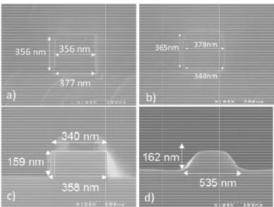
Fig. 3. SEM-c (c)) and with ( The sidewall the standard pattern heigh of 1.8 nm. A STRIP and R Si/SiO2 inter Fig. 4: Line (850°C/20To There is ther In this work, integrated in annealing pro cross section im ((b) and (d)) H2 ls roughness o conditions (c ht and an aver After annealin RIB respectiv rface limits the
edge roughne orr/2min): a) S efore a trade-o , we optimize n the passive ocess: temper mages of STRIP 2 annealing usin of the STRIP cf. Fig. 4). Wi age LER can g, the line ed ely. As expec e atomic surfa ess (LER) me STRIP case, b off between re the annealing circuit of th rature, time an P ((a) and (b)) a ng 850°C/20Tor
and RIB wav ith this techni be calculated dge of roughn cted, the roug ace migration easured by A b) RIB case educing the ro g conditions s he photonic c nd pressure. A and RIB ((c) an rr during 2 min veguides is ev que, the line . Before anne ess of the pat ghness reducti but it is at a c
FM along the oughness and
o that they are ircuit. As alr An increase in nd (d)) wavegui . valuated by AF edge roughne aling, both RI ttern are signi on is much m ost of profile e Si waveguid preserving the e compatible ready reported n temperature
ides profiles aft
FM before an ess (LER) can IB and STRIP ificantly decre more importan loss. de height befo e shape of the
with all types d [19], three or annealing ter patterning w nd after H2 an n be estimated P have similar eased of 55% nt in the RIB
ore and after e guides.
s of waveguid key paramet time, as well
without ((a) and
nnealing using d all along the average LER and 78% for case since no
H2 annealing
de architecture ters drive the as a decrease d g e R r o g e e e
Proc. of SPIE Vol. 10933 1093309-4
Downloaded From: https://www.spiedigitallibrary.org/conference-proceedings-of-spie on 10 May 2019 Terms of Use: https://www.spiedigitallibrary.org/terms-of-use
in hydrogen of guide stru pressure and After H2 ann is still of 0.4 the optimize roughness de reduced with annealing co 0.7nm). But optimized co with the opti losses that ar than 0.34 dB sidewalls rou with our sta degradation losses especi In this work, while keepin loss RIB and
Fig. 5. SEM annealing trea annealing cond pressure favo ucture (STRIP temperature, nealing optimi 43nm as for o ed conditions egradation tha h the optimize onditions, the they confirm onditions. Figu imized H2 an re reduced of B/cm are obta ughness is hig andard condit at the pattern ially for small we proposed ng satisfying p d STRIP wave cross section im atment; c) Line ditions. or the atomic P, RIB, Deep or long times zation, the en our standard m is similar to at can be obs ed conditions. LER of the to m that the LER
ure 7 shows th nealing condi f more than 70 ained for STR gher with the
tions and eve n bottom whic waveguides.
optimized H2
profile and dim eguides with lo mages of the R edge roughnes surface migra p RIB), it is n for milder co largement of t more aggressiv o the one obt
served at the . The AFM m op and middl R at the patte he optical loss itions. It clear 0% for both R RIP and RIB optimized con en better for ch is higher f 2 annealing co mensions. Th oss values at t RIB waveguide ss measured by ation. To obta necessary eith onditions in tem
the RIB botto ve conditions tained with th bottom of th measurement s e sidewalls is ern bottom is ses measured rly demonstra RIB and STRI waveguides, nditions, the o
the smaller for the standa onditions that e use of this o the best of the
e profiles after AFM along th ain optimal an her to favor s mperature and om dimension (cf. Fig. 5). C he standard c e pattern with shown in Fig s higher than s greatly impr at 1310nm fo ates the benef IP. Record los whatever the optical losses waveguide C ard conditions allow to smoo optimized trea state of the ar r encapsulation he RIB wavegui nnealing condi short times fo d pressure. is only of 50 Concerning, th conditions. H h the standard 6c indicates t for the standa roved from 1 or STRIP and
ficial impact o ss values of le eir width. Alt
of the STRIP CDs. This su s has a disastr oth RIB and S atment allowe rt. without (a) an ide sidewalls a itions adapted or aggressive nm while the he STRIP, the However, it se d condition ( that with the ard conditions .85nm to 0.76 RIB patterned of H2 anneali ess than 1.1dB though the av P waveguides uggests that th rous impact o STRIP wavegu ed us to fabric nd (b) with the fter etching and
d to any types conditions of average LER e profile with eems that the cf. Fig 6a) is optimized H2 s (1.06 nm vs 6nm with the d without and ing on optical B/cm and less verage STRIP are as low as he roughness on the optical uide sidewalls cate ultra-low e optimized H2 d optimized H2 s f R h e s 2 s e d l s P s s l s w 2 2
Proc. of SPIE Vol. 10933 1093309-5
Downloaded From: https://www.spiedigitallibrary.org/conference-proceedings-of-spie on 10 May 2019 Terms of Use: https://www.spiedigitallibrary.org/terms-of-use
Fig. 6: a) Tilte edge roughnes Fig. 7. Optical the optimized DOPT 2020 (DNRF-123) (648546) and [1] Marin-Pa “Microreson (2017). [2] Moss, D nitride and H ed SEM cross s ss measured by l losses measur H2 annealing. T internal fund ) center of ex d the Institut U alomo, P., K ator-based so D. J., Morando
Hydex for nonl
section images o AFM along the
red at 1310nm a The optical resu
ding program a xcellence silic Universitaire d Kemal, J. N., olitons for ma otti, R., Gaeta linear optics,’ of the STRIP w e STRIP sidewa as a function of ults for the stan
and the IRT N con photonics de France (IN R Karpov, M. assively parall a, A. L. and ’ Nat. Phot. P waveguide profi alls after the sta
f the waveguide dard H2 anneali FUNDING Nanoelec (CE s for commun L). EFERENCE , Kordts, A., lel coherent o Lipson, M., “ Papers 7(8), 59
iles after a) stan andard and opti
e width for a) S ing conditions a G EA-LETI and nications (SP ES , Pfeifle, J., optical commu “New CMOS 97 (2013). ndard and b) op mized H2 annea TRIP and b) R are also represe
LTM). Danis POC) (DTU). Pfeiffer, M. unications,” N S-compatible p ptimized H2 ann aling treatment IB patterned w ented in the STR sh Research C ERC H2020 H. and Ros Nat. Papers 54 platforms bas nealing; c) Line .
ithout and with RIP case. Council SPOC 0 GRAPHICS enberger, R., 46(7657), 274 sed on silicon e h C S , 4 n
Proc. of SPIE Vol. 10933 1093309-6
Downloaded From: https://www.spiedigitallibrary.org/conference-proceedings-of-spie on 10 May 2019 Terms of Use: https://www.spiedigitallibrary.org/terms-of-use
[3]Bakir, B. B., Descos, A., Olivier, N., Bordel, D., Grosse, P., Augendre, E. and Fedeli, J. M., “Electrically driven hybrid Si/III-V Fabry-Pérot lasers based on adiabatic mode transformers,’’ Opt. Exp. Papers 19(11), 10317-10325 (2011).
[4]Liao, L., Samara-Rubio, D., Morse, M., Liu, A., Hodge, D., Rubin, D. and Franck, T., “High speed silicon Mach-Zehnder modulator,’’ Opt. Exp. Papers 13(8), 3129-3135 (2005).
[5]Vivien, L., Rouvière, M., Fédéli, J. M., Marris-Morini, D., Damlencourt, J. F., Mangeney, J. and Pascal, D., “High speed and high responsivity germanium photodetector integrated in a Silicon-On-Insulator microwaveguide,’’ Opt. Exp. Papers 15(15), 9843-9848 (2007).
[6]Bogaerts, W., Selvaraja, S. K., Dumon, P., Brouckaert, J., De Vos, K., Van Thourhout, D. and Baets, R., “Silicon-on-insulator spectral filters fabricated with CMOS technology,’’ IEEE. J. Sel. Topics in quant. Elec., Papers 16(1), 33-44 (2010).
[7] Reed, G. T., “Device physics: the optical age of silicon,’’ Nat. Papers 427(6975), 595 (2004).
[8]Asghari, M. and Krishnamoorthy, A. V., “Silicon photonics: Energy-efficient communication,” Nat. Phot. Papers 5(5), 268 (2011).
[9] Levy, J. S., Gondarenko, A., Foster, M. A., Turner-Foster, A. C., Gaeta, A. L. and Lipson, M., “CMOS-compatible multiple-wavelength oscillator for on-chip optical interconnects,’’ Nat. Phot. Papers 4(1), 37 (2010).
[10] Luke, K., Dutt, A., Poitras, C. B. and Lipson, M.,“Overcoming Si3N4 film stress limitations for high quality factor ring resonators,’’ Opt. Exp. Papers 21(19), 22829-22833 (2013).
[11] Pfeiffer, M. H., Kordts, A., Brasch, V., Zervas, M., Geiselmann, M., Jost, J. D. and Kippenberg, T. J., “Photonic Damascene process for integrated high-Q microresonator based nonlinear photonics,’’ Optica, Papers 3(1), 20-25 (2016).
[12] Kim, S., Han, K., Wang, C., Jaramillo-Villegas, J. A., Xue, X., Bao, C. and Qi, M., “Dispersion engineering and frequency comb generation in thin silicon nitride concentric microresonators ,” Nat. Com. Papers 8(1), 372 (2017). [13] Streshinsky, M., Ding, R., Liu, Y., Novack, A., Yang, Y., Ma, Y. and Baehr-Jones, T., “ Low power 50 Gb/s silicon traveling wave Mach-Zehnder modulator near 1300 nm ,” Opt. Exp. Papers 21(25), 30350-30357 (2013).
[14] Michel, J., Liu, J. and Kimerling, L. C. “High-performance Ge-on-Si photodetectors,” Nat. Phot. Papers 4(8), 527 (2010).
[15] El Dirani, H., Casale, M., Kerdiles, S., Socquet-Clerc, C., Letartre, X., Monat, C. and Sciancalepore, C., “Crack-Free Silicon-Nitride-on-Insulator Nonlinear Circuits for Continuum Generation in the C-Band,” IEEE Phot. Tech. Lett. Papers 30(4), 355-358 (2018).
[16] Krückel, C. J., Fülöp, A., Ye, Z. and Andrekson, P. A., “ Optical bandgap engineering in nonlinear silicon nitride waveguides,’’ Opt. Exp. Papers 25(13), 15370-15380 (2017).
[17] El Dirani, H., Kamel, A., Casale, M., Kerdiles, S., Monat, C., Letartre, X. and Sciancalepore, C. “Annealing-free Si3N4 frequency combs for monolithic integration with Si photonics,” Appl. Phys. Lett. Papers 113(8), 081102-081105 (2018).
Proc. of SPIE Vol. 10933 1093309-7
Downloaded From: https://www.spiedigitallibrary.org/conference-proceedings-of-spie on 10 May 2019 Terms of Use: https://www.spiedigitallibrary.org/terms-of-use
[18] C. Bellegarde, E. Pargon, C. Sciancalepore, C. Petit-Etienne, V. Hughes, D. Robin-Brosse, J-M Hartmann, P. Lyan, “Improvement of Sidewall Roughness of Sub-Micron SOI Waveguides by Hydrogen Plasma and Annealing”,IEEE Photonic Techno. Letter 30, (7) 591-594 (2018)
[19] C. Bellegarde, E. Pargon, C. Sciancalepore, C. Petit-Etienne, O. Lemmonier, K. Ribaud, J-M Hartmann, P. Lyan, Optimization of H2 thermal annealing process for the fabrication of ultra-low loss sub-micron silicon-on-insulator rib
waveguides, Proc. SPIE 10537, Silicon Photonics XIII, 1053706 (2018);
Proc. of SPIE Vol. 10933 1093309-8
Downloaded From: https://www.spiedigitallibrary.org/conference-proceedings-of-spie on 10 May 2019 Terms of Use: https://www.spiedigitallibrary.org/terms-of-use


![Fig. 6: a) Tilte edge roughnes Fig. 7. Optical the optimized DOPT 2020 (DNRF-123) (648546) and [1] Marin-Pa “Microreson (2017)](https://thumb-eu.123doks.com/thumbv2/123doknet/13136629.388357/8.918.223.688.122.377/tilte-roughnes-optical-optimized-dopt-dnrf-marin-microreson.webp)
