HAL Id: tel-03088724
https://tel.archives-ouvertes.fr/tel-03088724
Submitted on 27 Dec 2020HAL is a multi-disciplinary open access archive for the deposit and dissemination of sci-entific research documents, whether they are pub-lished or not. The documents may come from teaching and research institutions in France or abroad, or from public or private research centers.
L’archive ouverte pluridisciplinaire HAL, est destinée au dépôt et à la diffusion de documents scientifiques de niveau recherche, publiés ou non, émanant des établissements d’enseignement et de recherche français ou étrangers, des laboratoires publics ou privés.
Magnetic Structures with Perpendicular Magnetic
Anisotropy
Xiaoxuan Zhao
To cite this version:
Xiaoxuan Zhao. Study of Interface Effects on Magnetization Reversal in Magnetic Structures with Per-pendicular Magnetic Anisotropy. Condensed Matter [cond-mat]. Université Paris Saclay (COmUE); Beihang university (Pékin), 2019. English. �NNT : 2019SACLS523�. �tel-03088724�
Etude des effets d'interfaces sur le
retournement de l'aimantation dans
des structures à anisotropie
magnétique perpendiculaire
Study of Interface Effects on Magnetization
Reversal in Magnetic Structures with
Perpendicular Magnetic Anisotropy
Thèse de doctorat de Beihang University et de l'Université Paris-Saclaypréparée à l’Université Paris-Sud
ED n°575 EOBE | Electrical, optical, bio-physics and engineering Spécialité de doctorat: Electronique et Optoélectronique, Nano-Microtechnologies
Thèse présentée et soutenue à Pékin, le 6 décembre 2019, par
Xiaoxuan Zhao
Composition du Jury : Arnaud Bournel
Professeur, Université Paris-Saclay Président Stéphane Mangin
Professeur, Université de Lorraine, Insitute Jean Lamour Rapporteur Jianhua Zhao
Professeur, Académie Chinoise des Sciences Rapporteur Tianxiao Nie
Professeur, Université de Beihang Examinateur Dafiné Ravelosona
Directeur de recherche CNRS, Orsay, C2N Directeur de thèse Weisheng Zhao
Professeur, Université de Beihang Co-Directeur de thèse
N N T : 201 9S A C LS 52 3
Acknowledgements
A journey in pursuit of PhD degree that witnessed excitements and frustrations, innovations and stupidities, etc. is to draw to a close. During this period, the difficulties and obstacles I encountered constantly urge me to strive and work hard. Without the help of my supervisors, my colleagues, my friends and my family, I would not be where I am today. Please allow me to extend my heartfelt thanks to all those people using this opportunity.
My doctoral study began in September 2016. I would like to give my sincere gratitude first and foremost to my supervisor Prof. Weisheng Zhao in Beihang University for offering me the opportunity to conduct my PhD research in his group. His consistent and illuminating instruction and belief in us endow me with confidence and courage to go through my PhD learning. His support for students can be found in many details. Even if I study abroad, when I am in trouble, I know very well that he is behind me.
During my second year in September 2017, I went to the lab of Centre de Nanosciences et de Nanotechnologies (C2N) in Université Paris-Saclay, where I met my co-supervisor, Prof. Dafiné Ravelosona. I sincerely appreciate him for he opened the door to the irradiation
technique for me and defined the research direction for my PhD thesis. I learnt a lot from him,
from how tiny magnets work and how to make a professional presentation to French idioms and authentic French culture. The time working with him in Paris is memorable and meaningful.
I am truly grateful to the members of my Thesis Defense Committee for their efforts to review my thesis. I sincerely give my thanks to the rapporteurs who wrote the reports for the manuscript and to the examiner and the president for their reading and evaluating my manuscript.
I would like to thank all the teachers and colleagues from Integnano group of C2N. I am especially grateful to Dr. Nicolas Vernier, Dr. Liza Herrera Diez and Mr. Sylvain Eimer. Most of my study in C2N was performed with the help of Dr. Nicolas Vernier, who taught me the knowledge of Kerr image microscopy and magnetic fundamentals. He is so enthusiastic and always ready to offer his kind help in both academic studies and daily life for me. Thanks go to Dr. Liza Herrera Diez in C2N, for she gave me valuable suggestions on my published paper, and also took much patience in revising it. Special thanks go to Mr. Sylvain Eimer, who cared for me when I was in Paris. Without him, my life in France would be less colorful.
Also thanks go to Mme Sophie Bouchoule, Mme Laurence Stephen and Prof. Eric Cassan from Doctoral School, for their assistance in my registration and thesis defense.
I am deeply indebted to all researchers and teachers in Beihang University, for their supports in my PhD research. Thanks go to all my colleagues and friends in the lab in Beihang University for their encouragement and company.
I would like to thank China Scholarship Council (CSC) for the financial support.
Finally, I am thankful to my family and relatives, especially my parents Mr. Xingzeng Zhao and Mrs Jing Liu. I am blessed to have parents who always unconditionally support and love me. I gratefully acknowledge their sacrifice for their only child. Then a big thank you goes to Dr. Hongchuan Wang, for his love and always back me up.
Xiaoxuan Zhao 08 October 2019, Beijing
CONTENTS
Abstract ... 1
Résumé ... 3
General Introduction ... 5
Chapter 1 Background and State-of-the-Art ... 7
1.1 Magnetic Random-Access Memory (MRAM) ... 7
1.1.1 Spin-transfer torque (STT)-MRAM ... 10
1.1.2 Spin-orbit torque (SOT)-MRAM ... 13
1.2 Domain wall dynamics ... 16
1.2.1 Field-driven DW motion ... 17
1.2.2 Spin orbit torque driven DW motion ... 21
1.3 Spin-dependent Interfacial effects in HM/FM/Oxide structure ... 22
1.3.1 Perpendicular magnetic anisotropy in HM-CoFeB-MgO structures ... 23
1.3.2 Interfacial Dzyaloshinskii-Moriya Interaction (DMI) ... 26
1.4 Summary ... 30
Chapter 2 Experimental Methods ... 31
2.1 Sample Fabrication ... 31
2.1.1 Ultra-thin film Sputtering ... 31
2.1.2 Magnetic Annealing ... 32
2.1.3 Hall bar Fabrication ... 33
2.1.4 Light-ion irradiation ... 35
2.2 Sample measurements and characterizations ... 38
2.2.1 Vibrating sample magnetometry (VSM) and superconducting quantum interference device (SQUID) for anisotropy measurements ... 38
2.2.2 Magneto-Optical Kerr Effect (MOKE) for Hysteresis Loop Measurements ... 39
2.2.3 Kerr miscopy for DW Imaging ... 40
2.2.4 Brillouin light scattering (BLS) for DMI measurements ... 43
2.2.5 Spin-dependent Electrical Transport Measurements ... 44
2.3 Summary ... 45
Chapter 3 Precise Modulation of Spin-Dependent Interfacial Effects ... 46
3.1 Modulation of magnetic anisotropy through different methods ... 46
3.1.1 FM thickness dependence of magnetic anisotropies ... 46
3.1.2 Dependence of magnetic anisotropy on sputtering ... 49
3.1.4 Ion irradiation for post-control of magnetic properties ... 54
3.2 Modulation of DMI through different methods ... 57
3.2.1 Dependence of DMI on FM thickness and annealing conditions ... 57
3.2.2 Influence of the interfacial disorder induced by irradiation ... 59
3.3 Summary ... 61
Chapter 4 Ultra-Efficient Magnetic Switching in W/CoFeB/MgO Structures through SOT 63 4.1 Ultra-low switching current in perpendicularly magnetized sample ... 63
4.2 Dependence of SOT switching on depinning field ... 66
4.3 Dependence of SOT switching on DMI ... 67
4.4 Influence of spin Hall angle on SOT switching ... 69
4.5 Summary ... 71
Chapter 5 Modulation of SOT Magnetic Switching in W/CoFeB/MgO Structures by Ion Irradiation ... 72
5.1 Enhancement of DW velocity through irradiation ... 72
5.2 Irradiation induced high-efficient SOT magnetization switching ... 75
5.3 Spin orbit torque driven multi-state resistance in irradiated Hall cross ... 77
5.4 Summary ... 84
Conclusions and Perspectives ... 85
General conclusion ... 85 Perspectives ... 86 Bibliography ... 87 List of Abbreviations ... 99 List of Publications ... 100 Résumé en Français ... 102
Abstract
Magnetic Random-Access Memory (MRAM), as one of the emerging technologies, aims to be a “universal” memory device for a wide variety of applications. The combination of the spin orbit torque (SOT) resulting from the spin Hall effect (SHE) and the Dzyaloshinskii– Moriya interaction (DMI) at interfaces between heavy metals and ferromagnetic layers has been demonstrated to be a powerful means to drive domain-wall (DW) motion efficiently, which is expected to be promising for the next generation of information carriers owing to ultra-low driving currents and ultra-fast DW motion. However, the crucial limitation of SOT induced DW motion results from the presence of pinning defects that can induce large threshold currents and stochastic behaviors. Such pinning defects are strongly related to structural inhomogeneities at the interfaces between the ultra-thin ferromagnetic layer and the other materials (insulator and/or heavy metals) that induce a spatial distribution of magnetic properties such as perpendicular magnetic anisotropy (PMA) or DMI. Therefore, understanding the role of the interface structure on DW motion and DMI is crucial for the design of future low power devices.
It is under this innovative context that my Ph.D. research focuses on the modulation of spin-dependent interfacial effects for efficient SOT switching. Based on the mainstream structures of MRAM, the interfacial anisotropy, DMI, DW motion and SOT phenomena in HM-CoFeB-MgO have been studied. The innovative approach shown in this thesis is the introduction of light ion irradiation to control the degree of intermixing at interfaces, for the modulation of spin-dependent interfacial effects. In W-CoFeB-MgO structures with high DMI, we have observed a large increase of the DW velocity in the creep regime upon He+
irradiation, which is attributed to the reduction of pinning centers induced by interface intermixing. Asymmetric in-plane field-driven domain expansion experiments show that the DMI value is slightly reduced upon irradiation, and a direct relationship between DMI and interface anisotropy is demonstrated. Using local irradiated Hall bars in SOT devices, we further demonstrate that the current density for SOT induced magnetization switching through DW motion can be significantly reduced by irradiation. Ultra-efficient SOT switching and multi-level resistances can be then obtained, providing a way to build up ultra-low power and high density spintronic devices for neuromorphic computing.
Résumé
Les mémoires MRAM (Magnetic Random Access Memory) sont l’une des technologies émergentes visant à devenir un dispositif de mémoire «universelle» applicable à une grande variété d’applications. La combinaison du couple de spin-orbite (SOT) résultant de l’effet Hall de spin (SHE) et de l’interaction de Dzyaloshinskii – Moriya (DMI) aux interfaces entre un métal lourd et une couche ferromagnétiques s’est révélée être un mécanisme efficace pour induire une propagation de parois magnétiques chirales à des faibles densité de courant. Les dispositifs à parois magnétiques devraient constituer la prochaine génération de supports d’information en raison de leur potentiel pour des densités de stockage très elevées.. Cependant, une limitation cruciale est la présence de défauts structuraux qui piègent les parois magnétiques et induisent des courants de seuil élevés ainsi que des effets stochastiques importants. L’origine du piégeage résulte de la présence de défauts structuraux aux interfaces entre la couche magnétique ultra-mince et les autres couches (isolants et/ou métaux lourds) qui induisent une distribution spatiale des propriétés magnétiques comme l’anisotropie magnétique perpendiculaire (PMA) ou le DMI. Comprendre l’influence de la structure des interfaces sur la propagation de parois et sur le DMI en particulier est cruciale pour la conception de futurs dispositifs basse consommation.
C’est dans ce contexte très novateur que mon doctorat s’est focalisé sur la manipulation de la structure des interfaces dans des couches ultra-minces à anisotropie magnétique perpendiculaire. Des structures de CoFeB-MgO ont été utilisées afin de mieux comprendre l'impact de la structure des interfaces sur l’anisotropie, le DMI, la propagation de parois et les phénomènes de SOT. L’approche innovante que nous avons utilisée est basée sur l’irradiation par des ions légers pour contrôler le degré de mélange aux interfaces. Sous l’effet du mélange induit par l’irradiation, nous avons observé dans des structures de W-CoFeB-MgO une forte augmentation de la vitesse de parois dans le régime de creep, compatible avec une réduction de la densité des centres de piegeage. Nous avons aussi démontré que l'anisotropie de l'interface Ki et le DMI mesuré par propagation assymmétrique de parois se comportent de la
même façon en fonction du mélange aux interfaces.
Finalement, nous avons fabriqué des barres de Hall afin de mesurer la commutation de l’aimantation induite par SOT. Le centre des croix de Hall a été irradié afin de diminuer localement l’anisotropie. Nous avons observé une réduction de 60% de la densité de courant critique après l’irradiation correspondant au retournement des croix de Hall irradiés par
propagation de parois. Notre étude fournit de nouvelles pistes concernant le développement de mémoires magnétiques à faible consommation, de dispositifs logiques et neuromorphiques.
Mots clés: Spintronics, interfaces, anisotropie magnétique perpendiculaire, parois
General Introduction
Spintronics, refers to the study of the electron spin in materials and devices that exploit the spin properties instead of (or in addition to) the charge degree of freedom. The development of spintronic technology together with other emerging technologies has brought the semiconductor industry to a “Beyond Moore” era. The study of the spin-dependent electron transport phenomena in ferromagnetic materials led to the discovery of the giant magnetoresistance (GMR) effect in the mid-80s, attributed to Peter Grünberg and Albert Fert who both received the Nobel Prize in physics in 2007, and the discovery of GMR is considered as the birth of spintronics. Due to its large magnetoresistance variation, GMR effect has successfully been integrated into read heads in hard-disk drives (HDDs) technology. The implementation of GMR in HDDs was followed by the discovery of CoFeB-MgO based magnetic tunnel junctions (MTJs) with tunnel magnetoresistance (TMR) ratio as high as 604%. This has led to the development of Magnetic Random-Access Memory (MRAM), a promising candidate for a universal memory, owing to its non-volatility, high switching speed, infinite endurance and ultimate density.
During the last decades, several generations of MRAM have been proposed depending on the writing schemes, including toggle MRAM controlled by a magnetic field, spin-transfer torque (STT) MRAMs that are currently on the market for embedded memory applications and the latest generation of spin-orbit torque (SOT) MRAMs that are the most promising in terms of low current density and high speed.
The typical structure for devices based on SOT switching is composed of a ferromagnetic layer (FM) in contact with a heavy metal layer (HM) and an oxide layer. In these structures, the interface effect becomes pre-dominant since the thickness of the layers is of the order or less than one nanometer. In this case, the magnetic anisotropy coming from the FM / Oxide and HM / FM interfaces favors an axis of easy magnetization perpendicular to the plane (PMA, perpendicular magnetic anisotropy). Another phenomenon that has drew great attention is the existence of an exchange coupling between the magnetic atoms and the atoms of the heavy metal, giving rise to the presence of the Dzyaloshinskii-Moriya interaction (DMI). This interaction is responsible for the existence of topological solitons such as chiral domain walls or skyrmions which can be moved very efficiently by SOT. On the other hand, the inhomogeneities at the interface induce a spatial distribution of the magnetic properties (PMA, DMI, ...), which can have an important influence on the processes of magnetization
reversal. A fundamental understanding of the interface structure on the magnetic properties is then a prerequisite to develop devices with high performances.
The main objective of this thesis is to study the modulation of spin-dependent interfacial effects and the efficient SOT switching. In order to modulate the structure of the interfaces, we have used in particular irradiation with light ions, which makes possible to control the structural properties of thin films at the atomic scale. We have used CoFeB-MgO thin films with PMA, which are the most promising materials for STT and SOT based devices.
The thesis is divided into five chapters as follows.
Chapter 1 is a presentation of the state-of-the-art of MRAM technology, as well as the basic principles for DW dynamics in films with PMA and a short description of interfacial effects in HM/FM/Oxide structures.
Chapter 2 presents the main experimental techniques used throughout this thesis for sample fabrication and characterization.
Chapter 3 is devoted to the study of influence of the interface structure on magnetic properties, like PMA and DMI. The influence of parameters related to the film growth process, post-annealing and ion-irradiation processes are thoroughly investigated.
Chapter 4 presents a SOT induced magnetic switching with ultra-low critical current in a perpendicularly magnetized structure. To provide a comprehensive understanding, spin Hall angle, DMI and DW dynamics are studied systematically.
Chapter 5 investigates the influence of interface intermixing induced by ion irradiation on SOT switching in devices based on Hall bar structures.
Chapter 1 Background and State-of-the-Art
This thesis aims at highlighting the influence of interfaces in ultra-thin magnetic films on PMA, DMI, DW motion and ultimately on magnetic switching induced by spin-orbit torque (SOT). The present chapter is devoted to providing a brief view of (i) MRAM technology, then introduces the mechanism of magnetization switching related to (ii) DW dynamics. Finally, the most important effects (iii) spin-dependent interfacial effects in HM/FM/Oxide structure are presented.
1.1 Magnetic Random-Access Memory (MRAM)
Memory is a key element in computer architecture, which can exert crucial influences on the speed, integration and power consumption of the device. Current computer systems are based on von Neumann architecture [1], as shown in Figure 1-1, including an arithmetic logical unit
(ALU), a control unit, a memory unit, and an input/output unit. However, continuously scaling down the complementary metal oxide semiconductor (CMOS) technology node drives high power and interaction latency issues due to the increasing leakage currents [2] and large
data traffic [3]. To overcome these power and latency issues, non-volatile computing memory
devices have received much attention in academic and industrial research [4-6]. Among
emerging non-volatile memories, MRAM has developed rapidly in the past few decades due to its fast speed, infinite endurance, and potential high density.
Figure 1-1. Configuration of von Neumann architecture.
In 1988, the discovery of giant magnetoresistance (GMR) in magnetic multilayers has highlighted a new path towards the design of spintronic devices based on manipulating both
the charge and spin of the electrons [7,8]. Afterwards, Tang et al. at IBM [9] proposed the
spin-valve as reading element in HDD, which has increased the data storage density of HDD by more than 1,000 times in one decade[10,11]. In the mid-1990s, a new magnetic device, the
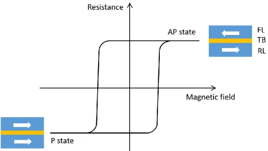
magnetic tunnel junction (MTJ), began to emerge, which became the key element of an MRAM cell. MTJ, as a multi-layer structure, consists of two ferromagnetic electrodes separated by an ultra-thin oxide layer. The magnetization of one of the ferromagnetic layers is pinned, while the other one can be switched under an external excitation. We call the former one reference layer (RL) and the latter free layer (FL). The oxide insulating layer is a tunnel barrier (TB). When the magnetizations of RL and FL are parallel, the MTJ stays in the low resistance (𝑅𝑃), whereas is the high resistance ( 𝑅𝐴𝑃), as shown in Figure 1-2. This corresponds to the binary system of “0” and “1”.
Figure 1-2. Schematic of the 2 states resistance depending on the relative magnetization directions of the RL and FL.
To measure the performance of MTJ, the tunnel magnetoresistance (TMR) ratio is defined as TMR =𝑅𝐴𝑃−𝑅𝑃
𝑅𝑃 . The higher the TMR ratio is, the higher the reading speed of the MTJ will be.
In a ferromagnetic material, the distribution of the spin-up and spin-down electrons is asymmetric around the Fermi level, as shown in Figure 1-3[12]. It is called the spin-dependent
tunneling and can be described by the spin polarization P = |𝑛↑−𝑛↓|
𝑛↑+𝑛↓, where 𝑛↑ and 𝑛↓ are
the density of electronic state of spin-up and spin-down near the Fermi level respectively. When the FL and RL stay parallel, the electrons in majority states in two layers have the same spin direction, resulting in a high tunneling probability, hence a high tunneling current and
Figure 1-3. Principle of spin-dependent tunneling. Figure from Ref [12].
Researchers have put tremendous efforts into the pursuit of high TMR ratio. Al2O3 was firstly
selected as the tunnel barrier [14,15], with typical TMR up to 18%. In 2002, first principles
calculation predicted that the TMR can be as high as 1000% by replacing Al2O3 with
monocrystalline MgO, due to its high matching degree with Fe ferromagnetic layers. Two years later, Parkin et al [16] and Yuasa et al [17] obtained a TMR of 220% in sputtered
CoFeB/MgO/CoFeB multi-layers. Up to now, the highest TMR based on the MgO tunnel barrier is 604%, realized in a CoFeB/MgO/CoFeB pseudo-spin-valve [18].
Thanks to a high TMR utilizing MgO tunnel barrier, MTJ-based MRAM has flourished since the last decade. So far, MRAM technology has gone through three generations depending on their writing schemes: magnetic field driven MRAM, STT driven MRAM and SOT driven MRAM, as illustrated in Figure 1-4.
Figure 1-4. Schematic diagrams of (a) field switching MRAM cell, (b) STT-MRAM cell and (c) SOT-MRAM cell. The white arrows in MTJs represent the direction of the magnetization in ferromagnetic layers. The black solid (dashed) lines with arrows represent the writing (reading) flows.
The first generation of MRAM uses magnetic field for the writing process, as shown in Figure 1-4(a). The in-plane MTJ is sandwiched in between a word line and a bit line, along the easy axis and hard axis of MTJ, respectively. The MTJ is selected to be written only if the word and bit lines corresponding to the junction are energized at the same time [19,20].However, this
technology has two main weaknesses, which limit its wide application. One is the high power consumption. A large current is required to generate the pulse of magnetic field during writing. Usually 7-10 mA/line is suitable for the required switching field [21]. The other is the narrow
write margin. A small current cannot switch the magnetization while a relatively large current may cause the misoperation of other MTJs, namely the half-selectivity disturbance. Although this problem was solved by Toggle MRAM [22], the magnetic field switching MRAM has been
left out due to its high power consumption and low integration.
1.1.1 Spin-transfer torque (STT)-MRAM
Thanks to the discovery of the spin transfer torque (STT) effect[23,24], a new generation of
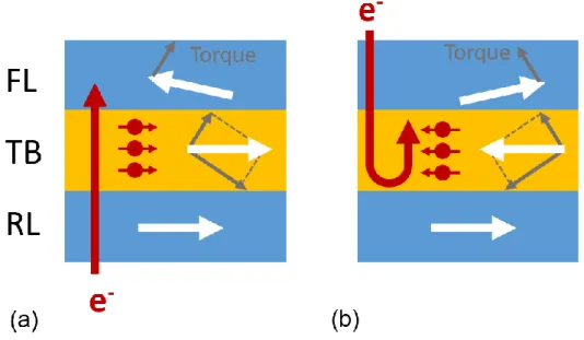
MRAM has been proposed and so far has attracted significant attention in research and development (R&D). As shown in Figure 1-4(b), a typical memory cell includes an MTJ and a transistor (1MTJ 1T). The basic operation principle of STT-MRAM is presented in Figure 1-5. When a current flows from the reference layer to the free layer (as seen in Figure 1-5 (a)), it is polarized and has the same spin angular momentum as the RL. The transverse component of the moment exerted on the magnetization of FL is like a torque, which is considered as spin transfer torque. This torque manipulates the FL magnetization to lie parallel to the reference layer. Similarly, current in the opposite direction flows from FL to RL, electrons with opposite spin direction of RL are reflected into the FL, facilitating an anti-parallel state of the FL and RL, as shown in Figure 1-5(b).
Figure 1-5. Illustrations of the basic operation principle of STT-MRAM. Write operation of the (a) parallel state (low resistance) and (b) anti-parallel state (high resistance).
The magnetization dynamics of the free layer resulting from the spin transfer torque can be expressed through the Landau-Lifshitz-Gilbert (LLG) equation by Macrospin approximation
[25,26]: 𝜕𝒎 𝜕𝑡 = −𝛾𝜇0𝒎 × 𝑯𝑒𝑓𝑓 + 𝛼𝒎 × 𝜕𝒎 𝜕𝑡 − 𝛾ℏ𝐽𝑃 2𝑒𝑡𝐹𝑀𝑠𝒎 × (𝒎 × 𝒎𝒓) (1.1)
where 𝒎 and 𝒎𝒓 are the unit magnetization of FL and RL, respectively; 𝛾 is the
gyromagnetic ratio; 𝜇0 is the permeability; 𝑯𝑒𝑓𝑓 is the effective field including the extra
field, demagnetized field and anisotropy field; 𝛼 is the Gilbert damping constant; ℏ is the reduced Planck constant; J is the writing current density; P is the spin polarization; e is the electron charge; 𝑡𝐹 is the thickness of FL and 𝑀𝑠 is the saturated magnetization of FL.
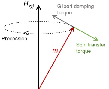
Three terms on the right side of the equation represent the effective field torque, Gilbert damping torque and spin transfer torque, respectively. The first torque induces precession of the magnetization vector around the effective magnetic field, while the damping torque and the collinear spin transfer torque compete with each other, as shown in Figure 1-6. As long as the current is larger than the threshold value, the transfer torque can circumvent the damping torque and induce a magnetization switching.
Figure 1-6. The magnetization dynamics under the effective field torque, Gilbert damping torque and spin transfer torque.
Compared to the first generation of MRAM using a magnetic field, STT-MRAM has been a significant discovery since it highlights a path towards the manipulation of magnetization with much less power and in a much more local way [27]. Thus, STT-MRAM has led to a
booming interest in the semiconductor industry during the last decade. In 2005, the first STT-MRAM chip using 65 nm node came out under the common efforts of Renesas Technology and Grandis Inc. [28]. In the same year, Sony Corporation of Japan released a 4
kbit STT-MRAM based on a 1MTJ 1T structure [29]. The magnetization of MTJ lied in the
sample plane, with an oval shape of 100×150 nm2, TMR of 160% and a critical switching
current 𝐽𝑐 of 2.5 × 10⁶ A/cm2. In 2007, Hitachi and Tohoku university launched a
STT-MRAM test chip with a storage capacity of 2 Mb. In this chip, not only the storage capacity has been greatly improved, the performance in terms of power consumption and reliability has also been enhanced. The unit writing energy consumption was only 1-2 pJ [30].
Three years later, Tohoku university successfully developed a magnetic tunnel junction with perpendicular magnetic anisotropy (PMA), expanding the device process node to sub-20 nm
[31]. In 2016, a perpendicular MTJ with 11 nm diameter STT-MRAM [32] was co-demonstrated
by IBM and Samsung, with an error rate of 7×10⁻¹⁰ at a write current pulse of 7.5 μA, 10 ns.
In the International Solid-State Circuits Conference (ISSCC) 2019, Intel announced that they were ready to ship the batch production of STT-MRAM with 22 nm FinFET process [33].
Despite this rising interest in the STT-MRAM, there are still some technical bottlenecks. From Figure 1-4(b), we can see that both the write and read currents flow through the MTJ, which will result in the aging of the MgO tunnel barrier, hence reduce the endurance and
reliability of the device [34]. Moreover, continuously scaling down of process node (< 45 nm)
can reduce the gap between the write and read currents, inducing undesirable writing when reading [35].
1.1.2 Spin-orbit torque (SOT)-MRAM
Recently, SOT switching magnetization has been proposed and attracted considerable attention [36,37]. This approach has practical implications for designing domain-wall based
memories or for three-terminal magnetic tunnel junction bits with the lateral writing current decoupled from the perpendicular readout current.
The basic structure of SOT-MRAM is a nonmagnetic heavy-metal stripe in contact with the free layer of MTJ. Because of the spin orbit coupling (SOC) in the heavy metal, a transverse current through the heavy metal stripe leads to a torque at the HM/FM interface, inducing the magnetization reversal. This spin orbit torque may arise from the Rashba effect [36,38,39] and/or
the spin Hall effect (SHE) [40-42], where the underlying physics is still under debate.
On the one side, Miron et al. considered that the Rashba interaction plays a key role in the reverse mechanism, which is induced by the asymmetric non-magnetic heavy metal and magnetic metal interface. When the current is injected in the plane of the HM, electrons experience an effective magnetic field
𝑯𝑹= 𝛼𝑅𝒛 × 𝑱𝒄 (1.2)
where 𝛼𝑅 is the Rashba constant, 𝒛 is a unit vector perpendicular to the film plane (the z
direction) and 𝑱𝒄 is the vector current density, as shown in Figure 1-7(a).
On the other side, Liu et al. hold that the spin accumulation induced by SHE is the intrinsic mechanism of the magnetization switching. In practical terms, when a current 𝑱𝒄 flows through the heavy metal, where the SOC is strong, the electrons of spin up and spin down will accumulate at the upper (or lower) and lower (or upper, depending on the spin Hall angle Θ𝑆𝐻𝐸 of the materials) interface, leading to a pure spin current 𝑱𝒔 along z axis:
𝑱𝒔 = Θ𝑆𝐻𝐸𝜎 × 𝑱𝒄 (1.3)
Figure 1-7. Three-terminal MTJ switched by spin orbit torque. (a) Induced by Rashba effect; (b) induced
by Spin Hall effect. Figure from Ref [12].
Despite the origin of the SOT, it can be quantified as an antidamping-like torque (𝝉𝑫𝑳 or 𝝉∥) and field-like torque (𝝉𝑭𝑳 or 𝝉⊥)[43-46]:
𝝉𝑫𝑳 (𝝉∥)~𝒎 × (𝒚 × 𝒎) (1.4)
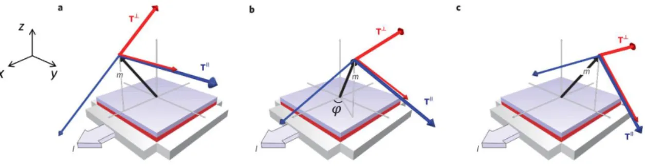
𝝉𝑭𝑳 (𝝉⊥)~𝒎 × 𝒚 (1.5) where 𝒎 is the magnetization vector, 𝒚 is the electron polarization direction vector of spin polarized current arising from SOC. Figure 1-8 presents the directions and amplitudes of 𝝉⊥ and 𝝉∥ corresponding to different directions of magnetization. In particular, the effective
magnetic fields produced by the two torques, 𝑩⊥ and 𝑩∥ are shown in Figure 1-8.
Figure 1-8. Torque schematics and magnetization measurements. The thick arrows indicate the direction
and amplitude of 𝝉⊥ (red) and 𝝉∥ (blue) for (a) 𝛗 = 𝟎°, (b) 𝛗 = 𝟔𝟎°, and (c) 𝛗 = 𝟗𝟎°. The thin arrows
Landau-Lifshitz-Gilbert (LLG) equation with two torque terms [47] added: 𝜕𝒎 𝜕𝑡 = −𝛾𝜇0𝒎 × 𝑯𝑒𝑓𝑓+ 𝛼𝒎 × 𝜕𝒎 𝜕𝑡 + 𝛾𝜇0𝐻𝑆𝑂𝑇 𝐷𝐿 𝒎 × (𝒚 × 𝒎) + 𝛾𝜇 0𝐻𝑆𝑂𝑇𝐹𝐿 𝒎 × 𝒚 (1.6) where 𝛾 is the gyromagnetic ratio; 𝜇0 is the permeability; 𝑯𝑒𝑓𝑓 is the effective field and
𝛼 is the Gilbert damping constant. 𝐻𝑆𝑂𝑇𝐷𝐿 and 𝐻𝑆𝑂𝑇𝐹𝐿 are the effective field induced by
damping-like torque and field-like torque, depicted as 𝐻𝑆𝑂𝑇𝐷𝐿 =𝐽𝑆𝑂𝑇𝜃𝑆𝐻ℏ
2𝑒𝑡𝐹𝜇0𝑀𝑠 (1.7)
𝐻𝑆𝑂𝑇𝐹𝐿 =𝜂𝐻𝑆𝑂𝑇𝐷𝐿 (1.8)
where 𝜃𝑆𝐻 is the HM spin Hall angle, ℏ is the reduced Planck constant, 𝑡𝐹 is the thickness of the adjacent FM layer, 𝐽𝑆𝑂𝑇 is the SOT current density, and 𝜂 is the ratio between the strength of these two torques.
The threshold SOT current density 𝐽𝑡ℎ derived from a quasi-static approximation is as
follows [48]: 𝐽𝑡ℎ =2𝑒𝑡𝐹𝑀𝑠 ℏ𝜃𝑆𝐻 ( 𝐻𝐾,𝑒𝑓𝑓 2 − 𝐻𝑥 √2) (1.9)
where 𝐻𝐾,𝑒𝑓𝑓 and 𝐻𝑥 represent the effective anisotropy field and in-plane field, respectively. It is worth noting that this formula is rather accurate with only DLT considered. However, despite that, to gain a low threshold current density, large spin Hall angle, thin FM layer and relatively low saturated magnetization are indispensable, which can be achieved by materials choices and interface manipulation.
The main challenge for SOT memory device is the requirement of an external magnetic field. From the schematic diagram of the SOT, only 90° switching can be realized with SOT. After SOT current is removed, the magnetization will randomly process to +z or -z direction because of thermal disturbance. Therefore, the injected SOT current itself cannot play a decisive role in switching for the perpendicular magnetization. An in-plane magnetic field along x axis is necessary to break the mirror symmetry and determine the switching direction
[38,40]. However, the external magnetic field not only increases the complexity of the device
design, but also increases the power consumption and reduces its reliability. This limits the development of SOT-MRAM. Therefore, how to use the spin orbit torque to directly reverse the perpendicular magnetization without external magnetic field has become one of the hottest issues. Currently, various methods have been proposed in order to realize the field-free switching. Some researchers employed the anti-ferromagnetic metal to replace the non-magnetic metal to provide SOT. The anti-ferromagnetic metal induces an exchange bias
along the writing current, equivalent to an external magnetic field [49,50]. In addition, ingenious
device geometry can also help realize the field-free switching [51]. The displacement of the
DWs observed in magnetic wires with different shapes and orientations is found to be highly dependent on the angle between the direction of the current and domain wall motion. Another approach consists in manipulating the structure of the interface. For example, different degrees of oxidation at the CoFeB/TaOx interface induce a torque along z axis, hence allowing
the switching of the perpendicular magnetization without external field [52]. The ability of
controlling the magnetization switching by manipulating the device geometry and film interface provides much of the early motivation for this thesis.
1.2 Domain wall dynamics
Magnetic domain is a basic phenomenon in magnetism. The investigation of domain wall dynamics is of importance for understanding magnetization switching. Meanwhile, the region between two uniformly magnetized domains, i.e magnetic DW, is the essence of the racetrack memory [53], which was proposed by IBM in 2008. Figure 1-9 shows the concept of racetrack
memory device, where a nanostrip is divided into magnetic domains separated by DWs (Figure 1-9 (c)). In such application, the up (blue) and down (red) domain represent the logic bit “0” and “1”. As an example, after 4 current pulses are injected into the nanowire, the pattern is shifted from 4 positions to the right. Domains can be moved back and forth depending on the polarity of the current flowing through the wire, as well as the spin Hall angle of the magnetic materials [54]. In this case, all DWs obtain the same speed due to
Zhang-Li torque [55], leading to the same domain width and negligible readout errors. This
concept is only valid under current pulses, while the external magnetic field will force the domains to align in the direction of the field and all the information will be erased.
Figure 1-9: Schematic of a racetrack memory device, representing a nanostrip divided into domains separated by DWs. The domains represent the logic bits “0” (blue) and “1” (red). (a) Initial states of the memory device. (b) After 4 current pulses, the whole bit pattern shifts 4 positions to the right. (c) Domain wall between two domains.
1.2.1 Field-driven DW motion
Understanding the dynamics of an elastic interface in presence of random disorder is a key issue in many physical systems. This is the case for a magnetic DW in a thin ferromagnetic layer with PMA driven by a magnetic field. It has been shown from theory [56-59] and
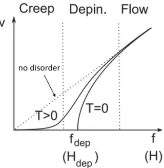
experiment [60-62] that 3 dynamical regimes of DW velocity versus magnetic field are
presented, as shown in Figure 1-10. At low applied fields, pinning due to structural defects dominates the DW dynamics, leading to a glass-like motion, which is the so-called creep regime described by universal power laws. In this region, pinning tends to stabilize DW positions [61], induce DW roughness, and introduce stochasticity [63]. At sufficiently high
magnetic fields, the DW propagates in the so-called flow regime where the velocity is proportional to the applied field and is limited only by intrinsic dissipation or friction-like force [64], i.e. the Gilbert damping parameter [65]. The region between the creep and flow
Figure 1-10. Theoretical velocity as a function of driving force at finite temperature (T > 0) and at T= 0. The creep, depinning, and flow regimes are labeled. In a “perfect” medium with no disorder, the velocity
is proportional to the driving force (dashed line). Image from Ref.[66].
In the thermally activated creep regime (f ≪ 𝑓𝑑𝑒𝑝, finite T), the velocity of the DW motion follows the creep law [60,67]:
𝑣 = 𝑣(𝐻𝑑𝑒𝑝, 𝑇) exp[−(𝑈𝑐 𝑘𝐵𝑇)(
𝐻𝑑𝑒𝑝
𝐻 )
𝜇] (1.10)
where 𝑣(𝐻𝑑𝑒𝑝, 𝑇) is a constant related to the depinning field 𝐻𝑑𝑒𝑝 at 0 K and the
temperature, 𝑈𝐶 is the scaling energy constant, kB is the Boltzmann constant, T is the
temperature, 𝐻 is the external applied field, and µ is the critical exponent. For a 1D DW propagating in a weak pinning disordered medium, µ=1/4 is in good agreement with the experiment data [57]. Since pinning dependent motion of elastic interfaces is observed in a
large variety of other systems [68] such as ferroelectric materials [69], contact lines in wetting [70], crack propagation [71], and earthquake models [72]., V. Jeudy et al. has proposed a unique
universal function in terms of pinning energy barrier to describe the creep law [68]:
𝑣 = 𝑣(𝐻𝑑𝑒𝑝, 𝑇) exp [− ∆𝐸 𝑘𝐵𝑇] (1.11) with ∆𝐸 = 𝑈𝐶[(𝐻𝑑𝑒𝑝 𝐻 ) 𝜇 − 1]. (1.12) For 𝐻 → 0, ∆𝐸 → 𝑈𝐶(𝐻𝑑𝑒𝑝 𝐻𝑒𝑥) 𝜇
and 𝑣 is in accordance with that described in Eq. (1.10). For 𝐻 → 𝐻𝑑𝑒𝑝, there is a linear vanishing of the energy barrier (∆𝐸 → 0), which indicates the upper boundary of the creep regime: 𝐻𝑑𝑒𝑝. According to Eq. (1.11-1.12), a linear
observed that the measured data for different films with PMA are in good agreement with the prediction of Eq. (1.10).
Figure 1-11. Natural logarithm of the DW velocity for Pt/Co/Pt films with four different Co thicknesses
plotted against H−1/4 that agrees with the creep theory prediction in Eq. (1.13). Image from Ref [66].
It is found that 𝐻𝑑𝑒𝑝 is also very important since it strongly depends on the structural
disorder of the magnetic films such as interface intermixing, interface roughness or grain boundaries [73]. R. Diaz Pardo and V. Jeudy et al. provided a fitting procedure to extract
𝐻𝑑𝑒𝑝[74]. In detail, the variation with temperature of the velocity at the threshold (H = Hdep)
can be written as:
𝑣 (𝐻𝑑𝑒𝑝, T) = 𝑣𝑇 ( 𝑇
𝑇𝑑𝑒𝑝)
Ψ (1.13)
while the variation with magnetic field at zero temperature (𝑇 ≪ 𝑇𝑑𝑒𝑝) is 𝑣 (𝐻, 𝑇 ≪ 𝑇𝑑𝑒𝑝) = 𝑣𝐻 (𝐻−𝐻𝑑𝑒𝑝
𝐻𝑑𝑒𝑝 )
β (1.14)
where 𝑣𝑇 and 𝑣𝐻 are depinning velocities, 𝑇𝑑𝑒𝑝 is a characteristic temperature related to
the pinning strength of the material, ψ and β are the critical exponents.
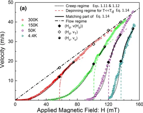
According to this method, the depinning field can be extracted by fitting Eq. (1.11-1.14). As an example shown in Figure 1-12, DW velocities in Pt/Co/Pt for different temperatures are measured. By fitting the universal creep law in Eq. (1.11) and the depinning law in Eq (1.13), depinning field could be extracted.
Figure 1-12. Domain-wall velocity in Pt/Co/Pt measured for different temperatures to show the high and
low drive regimes. The creep regime [0 <H <𝑯𝒅𝒆𝒑(𝑻)] is highlighted by the black dotted curves
corresponding to fits of Eq. (1.14) with μ = 1/4 and ends for velocities v (𝑯𝒅𝒆𝒑(𝑻), T) indicated by black
diamond symbols. The depinning regime extends from the depinning threshold H = 𝑯𝒅𝒆𝒑(𝑻) to the
universality limit Hu(T) (indicated by black solid spheres). The depinning velocities vT (𝑯𝒅𝒆𝒑(𝑻),T)
deduced from with part of all velocity curves as indicated by black solid segments. The linear flow regime, indicated by a straight dashed-dotted line, is Eq. (1.16) correspond to empty diamonds. Image from Ref.
[74] .
Since DW dynamics is sensitive to the structure inhomogeneous, it has been studied by introducing interface disorder. For instance, Herrera Diez et al. found that a significant decrease in DW velocity in creep regime was induced by ion irradiation in Ta/CoFeB/MgO thin films with PMA[73]. This could be explained by the interface disorder induced by
irradiation, which leads to a reduction of effective magnetic anisotropy and an extension of creep region of DW motion (corresponding to an increase of 𝐻𝑑𝑒𝑝). Later on, this group presented that the DW velocity was increased upon irradiation on the contrary in higher field region, namely the flow region, in the same film system [75]. This is an interesting result
because it seems to withstand the common perception that the flow area is not sensitive to disorders. Authors explained this from the aspect of the intrinsic parameters, which are strongly influenced by interface disorder. These studies clearly show that understanding the role of interface disorder is crucial for the design of future low power devices based on chiral DW motion.
1.2.2 Spin orbit torque driven DW motion
Successful control of DW motion under current is a necessary step toward the realization and scalability of DW devices such as the race track memory concept [53]. The current-induced
domain wall motion (CIDWM) in ferromagnetic nanowires has been intensively investigated since its first demonstration [23,24]. For a long period, CIDWM has been considered to be
driven by STT, including the adiabatic and nonadiabatic STTs [76,77]. However, it cannot
explain the direction of DW motion against the electron flow in Pt/Co/oxide structures [78-80].
In such structure with perpendicular magnetic anisotropy, the SOT induced by SHE and/or Rashba effect at the HM/FM interface have been proposed as a possible origin of CIDWM. The structure with PMA normally facilitates Bloch type DWs due to the existence of demagnetizing field, as shown in Figure 1-13 (a). In this scenario, the magnetization in the DW is collinear with the electron polarization direction y, making both 𝝉𝑫𝑳 and 𝝉𝑫𝑳 equal to zero. Hence, pure SOT current is incapable for driving DWs [81-83], while an in-plane field is
necessary. By applying such in-plane field, the magnetization in the DW is partially titled along x direction, according to what the nonzero SOT can act on the magnetization. However, as mentioned before, this external field must be removed from an application perspective.
Figure 1-13. The top view of the Bloch type (a) and Néel type (b) DWs in a perpendicularly magnetized
structure. The blue and red regions represent the down and up domains, respectively.
Later studies have shown that the effective DMI field has the capability of promoting and stabilizing the Néel type DWs [44,84,85], which can be competent to drive the SOT induced DW
motion. In this case, the magnetization in the DW aligns transversely with y direction, as shown in Figure 1-13(b). The combination of SHE, which produces current-induced torque, and the DMI, which stabilizes chiral DWs, induces uniform motion of Chiral DWs with rather high efficiency. The current generates an effective field associated by a Slonczewski-like torque [40,81], written as:
𝑯𝑺𝑳 = 𝐻𝑆𝐿∙ (𝒎 × (𝒛 × 𝒋𝒆)) (1.15) where 𝐻𝑆𝐿 is the effective torque field, 𝒎, 𝒛 and 𝒋𝒆 are unit vectors along the
experimentally confirmed the highly efficient DW motion induced by sole SOT in Pt/Co system [44]. Figure 1-14 presents this left handed Néel DWs with oppositely internal
magnetization for up–down and down–up transitions. The effective field 𝑯𝑺𝑳 that moves the
two DWs in the same direction against the electron flow is evidenced due to the sign of the Spin Hall angle.
Figure 1-14. Illustration of left-handed chiral Néel DWs. 𝑯𝑺𝑳 moves adjacent up–down and down–up
domains with velocity 𝒗𝑫𝑾 in the same direction against electron flow 𝒋𝒆. Image from Ref [44].
Magnetic skyrmion is another promising spin component, which can be regarded as a superposition of two bending DWs, hence can also be efficiently driven by SOT [87]. It is
considered to be more promising than chiral DWs as new information carriers in racetrack memory, due to its smaller size and lower depinning current density. However, the small size of skyrmion, usually in the range of several nanometers to several micrometers, is comparable to the size of structure inhomogeneous, such as extrinsic defects and grain boundaries. This makes the understanding and minimizing interface disorder a crucial topic and also provides the early motivation for this thesis.
1.3 Spin-dependent Interfacial effects in HM/FM/Oxide structure
By continuously scaling down the technological nodes, interfacial effects become even more apparent and play significant roles in spintronics. For example, in the SOT induced magnetization switching, the thickness of the cobalt layer is chosen to be 0.6 nm to maximize both the PMA and the Rashba effect due to structure inversion asymmetry at the platinum and AlOx interfaces [36]. In this thesis, we will highlight two interfacial effects: perpendicular
magnetic anisotropy (PMA) and Dzyaloshinskii-Moriya interaction (DMI) in in HM-CoFeB-MgO ultra-thin films, which attract great interest in current research on SOT.
1.3.1 Perpendicular magnetic anisotropy in HM-CoFeB-MgO structures
In a ferromagnetic material, the magnetization will be easier or harder to magnetize in terms of the direction, which is considered as the magnetic anisotropy. For most magnetically anisotropic materials, there are two favorable directions of spontaneous magnetization, and the two directions are a 180° rotation apart. The line parallel to these directions is called the
easy axis, along which the total energy of the material system will be the lowest. On the
contrary, the direction that facilitates the highest energy is the so-called hard axis. The energy consumed to rotate the magnetization from the easy axis to hard axis is the magnetic anisotropy energy (MAE).
The primary origin of magnetic anisotropy is the magnetic dipolar interaction and spin-orbit coupling. The dipolar interaction is a long-range effect, whose contribution is dependent on the shape of the sample, hence it is usually called the shape anisotropy. The spin-orbit coupling between the electron spin and orbit momentum leads to the anisotropy along different crystallographic orientations. It is referred to as the magnetocrystalline anisotropy
[88,89]. Besides, tension and/or stress could also lead to an anisotropy, which is called the
magnetoelastic anisotropy.
Shape anisotropy
When a particle is not perfectly spherical, the demagnetizing field will not be equal for all the directions, creating one or more easy axes. Thus, the shape anisotropy could be characterized by the demagnetizing field, as
𝑯𝒅 = −𝑵 ∙ 𝑴 (1.16)
where 𝑵 is the demagnetizing factor, which has three components ( 𝑁𝑥, 𝑁𝑦, 𝑁𝑧) in a three-dimensional object, and their relationship can be expressed as 𝑁𝑥+ 𝑁𝑦+ 𝑁𝑧= 1. For a thin film, the dimension of film thickness is much smaller than the film width and length. In this case, 𝑁𝑧 → 1, while 𝑁𝑥 and 𝑁𝑦 → 0.
The shape anisotropy induced magnetic anisotropy energy could be expressed as[90]
𝐸𝑑 = −𝜇0
2 ∫ 𝑴 ∙ 𝑯𝒅 𝑑𝑉 (1.17)
Considering the demagnetizing factor, the anisotropy energy density is
𝐾𝑑 = −2𝜋𝑀𝑠2 (1.18)
Magnetocrystalline anisotropy
The magnetocrystalline anisotropy of bulk materials with high symmetries such as Fe and Co is not as large as 10-6-10-5 eV/atom. But in the ferromagnetic systems, in which the FM1/FM2
anisotropy are consequently exhibited. The magnetocrystalline anisotropy energy density in such heterostructure could be as high as 10-4-10-3 eV/atom [91,92]. The magnetocrystalline
anisotropy from the bulk and interface both contributes to the total anisotropy.
Magnetoelastic anisotropy
Magnetoelastic anisotropy usually comes from the stress induced lattice mismatch, in which the stress could be caused by the temperature gradient and non-uniform deposition process, etc. The anisotropy caused by this effect is small and negligible.
In the ferromagnetic thin film, the effective anisotropy energy density could be expressed as: 𝐾𝑒𝑓𝑓 = 𝐾𝑏+ 𝐾𝑖/𝑡𝐹𝑀 + 𝐾𝑑
= 𝐾𝑏+ 𝐾𝑖/𝑡𝐹𝑀− 2𝜋𝑀𝑠2 (1.19) Thus, the total anisotropy energy can be expressed as:
𝐸𝑎𝑛𝑖 = 𝐾𝑒𝑓𝑓𝑡𝐹𝑀𝑆
= [(𝐾𝑏− 2𝜋𝑀𝑠2)𝑡𝐹𝑀+ 𝐾𝑖]S (1.20)
where S is the area of ferromagnetic film. From Eq. (1.20), we can see that the contributions from the bulk anisotropy 𝐾𝑏 increase with the growth of the FM thickness, while the interfacial contribution is independent of the thickness.
In 1985, P.F. Carcia et al. obtained the first perpendicular magnetic anisotropy (PMA) in Co/Pd multilayer structure when the thickness of Co is less than 0.8 nm. They attributed this to Co/Pd interface anisotropy and the stress effect in Co film [93]. Later on, the HM/FM/Oxide
structure has more widespread application prospect in MRAM since the oxide layer can be integrated in an MTJ with large TMR. In 2010, H. Ohno et al. observed the PMA in Ta/CoFeB/MgO layers when the thickness of CoFeB is less than 1.3 nm [31]. The effect
anisotropy constant 𝐾𝑒𝑓𝑓 can be expressed as: 𝐾𝑒𝑓𝑓 = 𝐾𝑏−𝜇0𝑀𝑠2
2 +
𝐾𝑖
𝑡𝐶𝑜𝐹𝑒𝐵 (1.21)
where 𝐾𝑏 is the bulk crystalline anisotropy and 𝐾𝑖 is the interfacial anisotropy, 𝜇0𝑀𝑠2
2 is the
demagnetization energy density and 𝑡𝐶𝑜𝐹𝑒𝐵 is the thickness of ferromagnetic layer CoFeB. Figure 1-15 illustrates the linear fitting of 𝐾𝑒𝑓𝑓∙ 𝑡𝐶𝑜𝐹𝑒𝐵 as a function of 𝑡𝐶𝑜𝐹𝑒𝐵. The slope of the linear extrapolation is 𝐾𝑏−
𝜇0𝑀𝑠2
2 , whose value is consistent with the calculated − 𝜇0𝑀𝑠2
2 ,
indicating that 𝐾𝑏 is negligible. Hence, the perpendicular anisotropy in this system is entirely
Figure 1-15. 𝒕𝑪𝒐𝑭𝒆𝑩 dependence of the product of 𝑲𝒆𝒇𝒇 and 𝒕𝑪𝒐𝑭𝒆𝑩, where the intercept to the vertical
axis and the slope of the linear extrapolation of the data correspond to 𝑲𝒊 and 𝑲𝒃−
𝝁𝟎𝑴𝒔𝟐
𝟐 . Circles and
squares are obtained from magnetization and FMR measurements, respectively. Figure from Ref. [31].
Later, theoretical evidence provided by the first-principles calculations shows that the O-𝑝𝑧 orbital around the Fermi level in MgO hybridized at the interface with the (𝑑𝑧2, 𝑑𝑥𝑧(𝑦𝑧))
orbitals of the transition metal Co and Fe[94,95] is the main contribution to the interfacial PMA.
Moreover, experiments have shown that another interface between FM and HM, also has huge impacts on PMA. In 2011, Worledge et al.[96] found that CoFeB/MgO bilayer deposited on Ta
exhibits PMA after annealing while on Ru does not. First-principles calculations reveal that at HM/FM interface, the hybridization of the Co (Fe) (𝑑𝑥𝑦, 𝑑𝑥2−𝑦2) orbitals and the (𝑝𝑦, 𝑝𝑧)
orbitals of the non-magnetic HM atoms also contribute to the PMA, and even generate stronger PMA than that at the CoFe/MgO interface [97,98]. The configuration of the invested
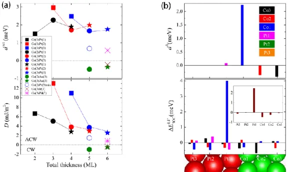
structures is shown in Figure 1-16 (a-d), the layer-resolved magnetic anisotropy energy (MAE) is calculated and depicted in Figure 1-16 (e) and (f). Different elements lead to quite different MAEs, which can be explained with the variations of SOC and orbital hybridizations at the CoFe/HM interface.
Figure 1-16. Schematics of atomic structures for a) MgO/CoFe/HM, b) MgO/CoFe, c) CoFe/HM, and d) CoFe thin films. e, f) Layer-resolved MAEs of different CoFe/HM structures. Nine CoFe monolayers (layer 1–9), five HM monolayers (layer 10–14), and a vacuum layer are included in the structures. Images
from Ref [97,98].
Apart from the term of material choices to tune PMA, experiment methods are also proved to be effective for that. In widely studied Ta/CoFeB/MgO structure, PMA highly relies on the annealing temperature. It is enhanced with the increasing temperature at first, however, when the temperature exceeds a certain degree, usually 350℃ for Ta-based structure, the film cannot remain PMA. This phenomenon could be explained by the element diffusion to the adjacent layer [99-103]. Moreover, the oxidation conditions (i.e. overoxidation or underoxidation) [104] at MgO/HM interface, stoichiometry of Co and Fe [105,106] and irradiation induced
interface disorder[73], also lead to a significant change in PMA. The influence of annealing
and irradiation on PMA will be discussed in more detail combined with our experiment results.
1.3.2 Interfacial Dzyaloshinskii-Moriya Interaction (DMI)
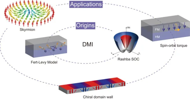
The interfacial Dzyaloshinskii-Moriya interaction (DMI) has attracted considerable interest recently due to its potential to the generation of skyrmions[107,108], stabilization of chiral
domain walls[44,109] and SOT induced switching[110]. Its main origins and applications are
Figure 1-17. A schematic illustration of the Dzyaloshinskii-Moriya interaction origins of DMI at different interfaces (inner ellipse) and the related performance properties of spintronic devices (outer ellipse).
In magnetic materials, the adjacent spin sites 𝑆𝑖,𝑗 tend to be parallel or antiparallel due to the Heisenberg exchange. The corresponding exchange energy can be written as [111]:
𝐸𝐻 = − ∑ 𝐽𝑖,𝑗 𝑖𝑗𝑺𝒊∙ 𝑺𝒋 (1.22) where 𝑺𝒊 and 𝑺𝒋 are neighbouring spins and 𝐽𝑖𝑗 is the corresponding exchange constant. When it is positive, interaction corresponds to ferromagnetic exchange, while the negative sign represents the antiferromagnetic exchange. In both cases, the exchange interaction is symmetric, that is to say, the right-handed chiral domain and the left-handed onehave the same energy. However, in a magnetic system with DMI, this symmetry is broken, indicating that two different chiral domains have different energies. The energy induced by DMI can be written as [112]:
𝐸𝐷𝑀 = ∑ 𝒅𝑖,𝑗 𝒊𝒋(𝑺𝒊× 𝑺𝒋) (1.23) where 𝒅𝒊𝒋 is the Dzyaloshinskii–Moriya vector, and it can be written as 𝒅𝒊𝒋 = 𝑑𝑖𝑗 ∙ (𝒛 × 𝒖𝒊𝒋).
𝒛 and 𝒖𝒊𝒋 are unit vectors, respectively perpendicular to the film plane and pointing from site i to site j. For 𝑑𝑖𝑗> 0, the chiral spins tend to be arranged like ↑→↓, namely clockwise rotations from 𝑆𝑖 to 𝑆𝑗. We denominate it the right-handed chirality. Correspondingly, the
left-handed chirality favors the anticlockwise ↑←↓ spin [113-116].
In HM/FM/Oxide structures, the DMI is considered to arise from two different origins, the Fert-Levy model at FM/HM interface [117,118] and the Rashba spin-orbit coupling at FM/Oxide
interface [119,120].
resulting in a DMI vector perpendicular to the plane of the triangle formed by the three atoms and along the FM/HM interface. This 3-site indirect exchange mechanism which can be used to describe the DMI at FM/HM interface is referred to as the Fert-Levy model [107,117,118].
According to a calculation utilizing Vienna Ab-initio Simulation Package (VASP) [121], layer
resolved DMI for Co (3)/Pt (3) bilayers and the distribution of the SOC energy are presented in Figure 1-18. It can be found that the predominant contribution of the large total DMI is attributed to the isotropic exchange coupling between the interfacial Co and Pt atoms. And the total DMI is decreased when intermixing between Co and Pt layers at interface occurs. The large DMI strength between spins of the interfacial Co atoms originates from the large SOC energy change in the adjacent interfacial Pt layer which is consistent with the Fert-Levy model [122]. Moreover, Belabbes A. et al. calculated the chemical trend of DMI for a series of
3d transition metals deposited on different 5d heavy metals using the first-principles
calculations with the FLAPW method [123]. They attributed the DMI changes at various
FM-HM interfaces not only related to the strength of spin-orbit coupling in the 5d heavy metals but also to the orbital hybridization between the 3d states and the 5d states around the Fermi level at the interface. It is controlled by the Hund’s exchange field of 3d states of the magnetic transition metals according to the Hund’s first rule. In more detail, the spin-flip mixing of the 3d orbital states and the electron hopping with the intermediate spin-orbit active 5d states play a significant role in controlling the sign and the strength of DMI.
Figure 1-18. (a) Schematic of the total DMI parameter 𝒅𝒕𝒐𝒕 and the micromagnetic DMI coefficient D of
the Co/Pt bilayers (b) Sketch of the layer resolved DMI parameter 𝒅𝒌 for Co(3)/Pt(3) bilayers and the
DMI ∆𝑬𝑺𝑶𝑪
𝒕𝒐𝒕,𝒌′. Image from[121].
In addition, it has been shown that the interface of FM and oxide [119,120], even graphene [124], could also induce DMI. Such DMI cannot be explained by the hybridization between 3d states of the magnetic transition metal and 5d states of heavy metal around the Fermi level. Yang et.
al [120] reported a 60 percent increase of DMI in Pt/Co/MgO structures compared to Pt/Co
bilayers. Moreover, according to the Ab initio calculation, at the interface of MgO/Co, the SOC energy is located in the interfacial Co, rather than the 5d heavy metal, indicating a different mechanism from the HM/FM interface. Since metal and oxygen ions carry large positive and negative charges, the oxide compounds are naturally highly ionic [125]. This
property with the combination of the breaking inversion symmetry, results in an embedded electric field along the normal direction of the interface, and SO interaction is at the essence of the so-called Rashba effect [126]. Usually we regard the partial Rashba Hamiltonian as
𝐻𝑅 =𝛼𝑅
ℏ 𝝈 ∙ (𝒑 × 𝒛), which is supposed to break the structural inversion symmetry
[47,127-130].
By taking into account the Rashba coefficient 𝛼𝑅, Yang et. al [120] calculated the Rashba
splitting for the MgO capped 3 ML of Co, getting the value of 𝑑𝑡𝑜𝑡 between 0.81 and 1.55
meV. This smaller value, compared with their DFT results of 1.88 meV, could be attributed to the fact that the Rashba-type DMI was calculated by using only one band close to Fermi level, but in fact other bands from Fermi level may also contribute to the total DMI. Belabbes et
al.[131] further studied the physical mechanism of the DMI at Oxide/FM interface by
calculating the control of DMI through interface oxidation using density-functional theory (DFT) with FLAPW method as implemented in the FLEUR code. They used the system of O/Fe/Ir (001) to explore the impact of the surface oxidation on DMI, and drew a conclusion that the sign and the strength of DMI strongly depend on the charge transfer and related hybridization between 2p-O and 3d-Fe states around the Fermi level which induces an electric surface dipole moment. In other words, the DMI of Oxide/FM structures is related to a large charge transfer and the large interfacial electric field that compensates the small spin-orbit coupling of the atoms at the interface.
Tunable DMI in Pt/Co/MgO structure is studied due to its high SOC at the interface. By inserting a dust of Mg between Co/MgO interface, DMI can be strongly enhanced by 5 times with the increasing MgO thickness, due to the increase of Co-O band [132]. For the
HM/CoFeB/MgO system, the induced DMI is slightly inferior, but there are more possibilities influencing interfacial DMI. Torrejon et al.[133] and Gross et al. [115] controlled the interfacial
structure. Moreover, thermal annealing is found to be helpful for enhancing DMI in Ta/CoFeB/MgO due to the diffusion of B atom, similar to the mechanism of PMA.
1.4 Summary
In this chapter, we have reviewed the different concepts of MRAM technology and in particular we have discussed the importance of DMI and SOT in DW based devices driven by currents. We have also highlighted the important impacts of interface conditions on spin-dependent interfacial effects, such as PMA and DMI, as well as DW dynamics.
Chapter 2 Experimental Methods
In this chapter, the fabrication and characterization techniques used in this PhD research will be introduced. The first part will describe the sample fabrication process, including film deposition, annealing, Hall bar fabrication process flow, and in particular light-ion irradiation, which is a useful method to control magnetism at the atomic scale. The relevant and useful characterization techniques we have used will be described in the second part. These techniques include characterization of the thin film morphology, magnetization, and electrical transport properties.
2.1 Sample Fabrication
2.1.1 Ultra-thin film SputteringHeavy metal (HM)/ ferromagnetic metal (FM)/oxide heterostructure with perpendicular magnetic anisotropy (PMA) has a great potential to hold high thermal stability, large TMR value and low critical switching current, which are required for the MRAM [31]. To optimize
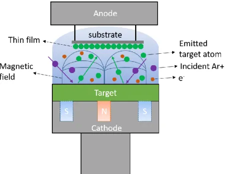
the performance of this structure, high quality thin films with an accurate control of the film thickness is the key point. During the past few decades, magnetron sputtering has been widely used in both industrial and academic domains, as it can provide high growth rate, relatively good yield, and precise thickness control at the atomic scale over 300 mm wafer [134,135].
Magnetron sputtering is a kind of Physical Vapor Deposition (PVD) technique. Figure 2-1 shows the schematic diagram of the sputtering process. With the presence of electric field (between the anode and cathode), the electrons are accelerated and collide with the incident argon atoms. The ionized argon ions (Ar+) then strike the target surface with extremely high
energy under the effect of electric field. Finally, the sputtered target atoms fly towards the substrate allowing the growth of a thin film at an atomic scale. Note that usually a magnetic field is also applied in addition to the electric field to force the electrons to move spirally by Lorentz force, hence increasing the chance of electrons to collide with the Ar gas.
![Figure 1-3. Principle of spin-dependent tunneling. Figure from Ref [12] .](https://thumb-eu.123doks.com/thumbv2/123doknet/14528541.723222/17.892.289.610.117.507/figure-principle-spin-dependent-tunneling-figure-ref.webp)