HAL Id: hal-02130590
https://hal.archives-ouvertes.fr/hal-02130590
Submitted on 15 May 2019HAL is a multi-disciplinary open access archive for the deposit and dissemination of sci-entific research documents, whether they are pub-lished or not. The documents may come from teaching and research institutions in France or abroad, or from public or private research centers.
L’archive ouverte pluridisciplinaire HAL, est destinée au dépôt et à la diffusion de documents scientifiques de niveau recherche, publiés ou non, émanant des établissements d’enseignement et de recherche français ou étrangers, des laboratoires publics ou privés.
Unconventional Nanofabrication for Supramolecular
Electronics
Yifan Yao, Lei Zhang, Emanuele Orgiu, Paolo Samorì
To cite this version:
Yifan Yao, Lei Zhang, Emanuele Orgiu, Paolo Samorì. Unconventional Nanofabrica-tion for Supramolecular Electronics. Advanced Materials, Wiley-VCH Verlag, In press, �10.1002/adma.201900599�. �hal-02130590�
1
Unconventional nanofabrication for supramolecular electronics
Yifan Yao,1 Lei Zhang,2* Emanuele Orgiu,3 Paolo Samorì1*
1 Dr. Y. F. Yao, Prof. P. Samorì
University of Strasbourg, CNRS, ISIS UMR 7006 8 allée Gaspard Monge, F-67000 Strasbourg, France E-mail: [email protected]
2 Prof. L. Zhang
Key Laboratory of Mesoscopic Chemistry of MOE, School of Chemistry and Chemical Engineering, Nanjing University
Nanjing, Jiangsu 210023, China E-mail: [email protected] 3 Prof. E. Orgiu
Institut national de la recherche scientifique (INRS), EMT Center, 1650 Blvd. Lionel-Boulet, J3X 1S2 Varennes, Québec, Canada.
E-mail: [email protected]
2
Abstract
The tremendous scientific effort devoted to achieving a full control over the correlation between structure and function in organic and polymer electronics, has prompted the use of supramolecular interactions to drive the formation of highly ordered functional assemblies, which have been integrated into real devices. Such endeavour gave birth to the field of supramolecular electronics. In this regard, self-assembly of organic semiconducting materials constitutes a most powerful tool to generate low-dimensional and crystalline functional architectures. These include 1D nanostructures (nanoribbons, nanotubes, and nanowires) and 2D molecular crystals with tuneable and unique optical, electronic and mechanical properties. Optimizing the (opto-)electronic properties of organic semiconducting materials is imperative to harness such supramolecular structures as active components for supramolecular electronics. However, their integration in real devices currently represents a significant challenge to the advancement of (opto)electronics. In this progress report, we provide an overview of the unconventional nanofabrication techniques and device configurations, which were devised during the last decade, to enable supramolecular electronics to become a real technology. In particular, we will highlight how single and multiple supramolecular fibers and gels as well as supramolecularly engineered 2D materials can be integrated into novel vertical or horizontal junctions to realize flexible and high-density multifunctional transistors, photodetectors and memristors, exhibiting a set of new properties and excelling in their performances.
3
1. Introduction
Optoelectronics is field of fundamental science and technology which combines electronics and light. The integration of organic molecules in opto-electronic devices holds unique advantages over their inorganic counterpart, as a result of the tunable chemical and physical properties of the compounds and materials thereof, light-weight and bendability.[1-7] However,
a clear prerequisite towards the use of semiconducting organic molecules in opto-electronics consists in the need of boosting their charge carriers mobility. The mobility is largely dominated by the motif and the degree of order of the molecular assembly, as well as the grain boundaries between crystalline domains and the trap density.[8-10] Fortuitously, all four factors
can be tuned and improved simultaneously by exploiting the immense opportunity offered by supramolecular self-assembly: π-conjugated molecules can self-organize into virtually boundary-free and highly ordered low-dimensional supramolecular aggregates with pseudo- and/or poly-crystalline domains,[11-14] which could thermodynamically exclude the impurity
molecules serving as the dopant and traps.[15] The effort to integrate those supramolecular
nanostructures as charge transporting layers in electronic devices led to the emergence of supramolecular electronics, which was first conceptualized by Schenning and Meijer[16,17] as
bridging the gap between single molecules (Å) and macroscopic thin-film organic electronics (> μm) on a scale of hundreds of nanometers. Here, we propose to refine such a definition by considering supramolecular electronics as the branch of electronics that is based on non-covalent molecular architectures extending over one or two dimensions, i.e. whose width and/or thickness range from that of a single molecule up to the 10-nm scale (Scheme 1). 1D nanostructures such as nanowires, nanofibers, nanorods, nanobelts, nanoribbons and nanotubes are highly anisotropic: they possess a lateral dimension on the 1-100 nm scale and a length of orders of magnitude greater. 2D nanostructures are ultrathin architectures with a thickness on the atomic or molecular scale and a much larger lateral dimension. Supramolecular electronics indeed relies on bottom-up nanostructures held together through weak intermolecular forces such as van der Waals, hydrogen or halogen bonds or π-π interactions. A great deal of supramolecular architectures displaying a relatively high degree of order can be finely assembled under thermodynamic control,[18,19] by solution processing under mild conditions
such as room temperature and pressure. In the past decades, significant progress has been made in designing novel low-dimensional supramolecular structures, such as gels, soft nanoribbons, nanotubes, and nanowires.[20-26] Besides assembling highly organized nanostructures, a major
4
such structures with electrodes. Hitherto, a moderate attention has been paid to this crucial issue. It is true that the wiring-up of discrete and anisotropic nano/microstructures is challenging because of the architecture’s intrinsic brittleness (e.g. nanocrystals) and of their tendency to break when traditional micro- and nano-fabrication methods such as electron beam lithography, photolithography or focused ion beams are used.
In this progress report, we first introduce the recent progress on charge transport in low-dimensional supramolecular architectures while emphasizing their suitability for applications in optoelectronics. Then, we highlight the most enlightening approaches and unconventional patterning techniques that have been exploited to precisely integrate functional supramolecular assemblies into macroscopic devices/circuits. We finally provide some outlooks proposing concepts which may enable the field to be leveraged in the future into a real supramolecular electronic technology.
Scheme 1. Overview of representative (semi)conducting structures integrated into electrical
devices. Supramolecular electronics is based on 1D or 2D highly ordered non-covalent assemblies displaying a width and/or thickness in the 1-10 nm range combined with tunable optical and electronic properties.
2. Charge transport in low-dimensional supramolecular aggregates
The availability of ordered supramolecular nanostructures is a prerequisite towards the exploration of the structure-property relationships in π-conjugated materials. Before the enumeration of supramolecular nanostructures, we need to introduce some common device configurations and key parameters currently employed to characterize organic semiconductors. Field-effect transistors (FETs) are three terminal devices comprising a semiconducting layer, a dielectric layer and three electrodes (drain, source and gate). FETs represents the archetypical electrical device which enables to explore the charge carriers transport characteristics of
self-5
assembled supramolecular materials which can be used as the semiconducting layer. The figures of merit used to evaluate the device performance are typically field-effect mobility (μFET, expressed in cm2 V-1s-1), Ion/Ioff and threshold voltage (Vth, expressed in V). In detail, the
mobility is defined to be the drift velocity of carriers under unit electric field, Ion/Ioff is the ratio
between the maximum on-state current to the minimum off-state current, and the threshold voltage is the minimum gate voltage that is required to turn on the transistor. To investigate the photo response of supramolecular materials, a light with a given wavelength is shone onto FETs that would then act as phototransistors (three-terminal devices). When a current is measured on a two-terminal device as a function of the light irradiation, that device is called
photodetector. Similarly, phototransistor is a three-terminal device with the light control acting
as the “fourth terminal”. To characterize photodetectors and phototransistors, several key performance indicators are used such as photosensitivity (P) and responsivity (R). The photosensitivity P can be defined as P = $%&'()*$+,-.
$+,-. , where Ilight and Idark are the drain current
under illumination and in dark, respectively. The photoresponsivity can be defined as R =
$%&'()*$+,-.
0×2& , where Pi is the incident light intensity (expressed in W/cm
2), and S is the effective
device area. Photoresponsivity is the signal to noise ratio of photocurrent to dark current. Responsivity is the effectiveness of a photodetector to convert an optical signal into an electrical one.[27] Spectral response range (the range of light wavelength that the photodetector
can detect), response time, and external quantum efficiency (EQE) (the ratio of photoelectrons produced by the incident photons to the number of incident photons) are also key important parameters for optoelectronic devices.[28]
2.1 One dimensional (1D) self-assembled nanostructures
1D nanostructures are appealing because of their unique (opto-)electronic properties such as large charge carrier mobilities, high electronic conductivities and abundance of interfaces for exciton separation and charge transfer. Furthermore, the ordered arrangement at the supramolecular level and the high surface-to-volume ratio of 1D nanostructures make them extremely sensitive to the external stimuli. Suitably designed π-conjugated organic molecules are prone to undergo spontaneous bottom-up self-assembly, primarily ruled by π-π stacking, forming semiconducting materials such as highly crystalline 1D nanostructures (e.g., nanowire, nanobelt and nanotube).[20,22] In the past few years, a great deal of effort has been devoted to
6
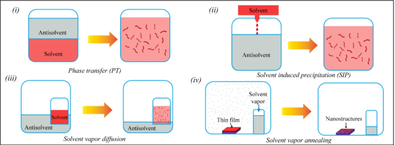
of π-conjugated organic materials into 1D nanostructures under ambient conditions (Figure 1).[29] This includes processing methods such as solvent phase-transfer (PT),[30-32]
solvent-induced precipitation (SIP),[26,33-38] solvent-vapor diffusion (SVD),[39] and post processing
methods like solvent-vapor annealing (SVA).[40,41] All of these processing strategies aim at
forming a dynamic balance between the orthogonal good and poor solvent (or vapor) which can be subtly adjusted by means of external parameters. For example, SIP allows to form a large number of highly ordered 1D nanofibers by simply mixing of the molecular building blocks with suitable non-solvents at appropriate concentration and temperature, as shown in Figure 1 ii. By operating under thermodynamic control, the SVA process of self-assembly enables to minimize structural defects in the assembly and boost the degree of crystallinity in the produced nanostructures. Significantly, the properties of these nanostructures including the crystalline degree, size and softness could be further tuned by modifying the surface deposition parameters (concentration, pH, temperature, etc.) and by carefully choosing the solvents.[17,42]
Alongside, also post-processing methods such as solvent-vapor annealing and thermal annealing can be exploited to improve the self-assembly directly on the solid-state (Figure 1 iv).[41,43,44]
Figure 1. Diagrams illustrating some relevant approaches that can be pursued to control the process of molecular self-assembly: (i) Phase-transfer method; (ii) Solvent-induced precipitation (iii) Solvent-vapor diffusion; (iv) Solvent-vapor annealing.
Two- and three-dimensional structures has clear advantages when exploited as semiconducting materials in organic field-effect transistors (OFETs): the percolation pathways around any structural and electronic defect, which is guaranteed by the dimensionality, ensures efficient charge transport at the materials level, thereby high charge carriers mobilities. Conversely,
one-7
dimensional organic semiconducting nanostructures formed via self-assembly offer modest charge transport characteristics which are however combined with unique additional features such as vectorial properties and flexibility.[42,45-47] The exemplary case is the one of
perylenetetracarboxyldiimide (PDI) nanowires produced via solution-phase self-assembly, which have been demonstrated as the n-channel semiconductor in OFETs and as building-blocks in high-performance complementary inverters as shown in Figure 2a.[30] The PDI-C
n
nanowires were produced by SIP, simply upon adding methanol (bad solvent) to the solutions of PDI-Cn in chloroform (good solvent); by shifting the equilibrium from solvation to
molecular aggregation via intermolecular π-π interactions, the generated nanostructures precipitate leading to the formation of nanowires completed within several minutes (Figure 2a, i). Single-crystal X-ray characterization revealed that the PDI-C8 molecules exhibit slipped π-π stacking along the [100] direction (long needle direction), as shown in Figure 2a ii. Charges transport through such quasi one-dimensional nanostructures can be significant only along the main axis of the wire, because the overlap of the molecular π orbitals is crucial for the charge transport in organic semiconductor materials.[48,49] The PDI nanowires based OFET devices are
fabricated by directly drop-casting its methanol suspension onto the gold pre-patterned electrodes supported on a dielectric surface. Output characteristics of transistors fabricated from PDI-C8 and hexathiapentacene (HTP) nanowires together with a colorized SEM image of a network of PDI-C8 nanowires as shown in Figure 2a, iii and iv. From the saturation-regime transfer plots, electron mobilities of 6.9 ± 2.7×10⁻⁵, 7.2 ± 7.0×10⁻³, and 6.7 ± 3.0×10⁻³ cm2 V -1s-1 were achieved for PDI-C5, -C8, and -C13, respectively. Briseno et al. also successfully
demonstrated the fabrication of complementary inverters by incorporating p-channel HTP and n-channel PDI nanowires as active components, with gain values of 8. The modification of the side chain structures, makes it possible to tune the π-π stacking arrangement thus allowing to study the structure-property relationship in molecular assemblies.[50-53] Alongside PDI, other
molecules possessing rigid aromatic cores, such as fluorenes, anthracenes, hexabenzocoronenes (HBCs) and sulphur-based heterocycles exhibit planar π-conjugated systems which can also undergo self-assembly forming low-dimensional nanostructures.[54-58]
Compared to small molecule semiconductors, conjugated polymers are much more difficult to controllably self-organize into highly ordered nanoscale architectures. The finite rigidity of macromolecules, which can be quantified by means of their persistence length, notoriously hinders the process of crystallization since large and multiple free energy barriers needs to be overcome during the self-assembly process.[59-61] So far, several highly crystalline conjugated
8
polymers with long-range molecular packing, free grain boundaries and minimized defects have been obtained by making use of an ultraslow self-assembly process from dilute solutions in an ambient saturated by certain solvent-vapors.[62-68] Dong et al. systematically investigated
the correlation between molecular order/orientation and charge transport properties by using a rigid-rod conjugated polymer, poly(para-phenylene ethynylene)s derivative (TA-PPE), as exemplified in Figure 2b.[63] The characterization by selected-area electron diffraction (SAED)
provided evidence for the single crystalline nature of the assembly. Further structural analyses suggested the nanowires exhibit an orthorhombic crystal unit cell structure and the backbones of TA-PPE chains are parallel to the long axis of nanowire with their side chains standing on the substrate plane. The transport properties of the nanowires were characterized by fabricating and testing the OFETs, which displayed hole mobility of ca. 0.1 cm2 V-1s-1, being 3-4 orders
higher than that of spin-coated thin-film transistors. Such improvement can be ascribed to the interplay of efficient intrachain transport along the stretched polymer backbone and the reduced structural defects enabling more efficient interchain transport. More recently, another bottom-up strategy has been devised for the production of highly crystalline conjugated polymers nanostructures. In this case the crystallization process does not start from the polymer chains but from their corresponding reactive monomers. In essence, the transformation of the monomer crystal to a polymer crystal is carried out in-situ in the solvent-state to finalize the polymerization process.[69,70] To illustrate the strategy, an asymmetric diacetylene (DA)
precursor of 10,12-pentacosadiynoicacid (PCDA) was used as model system, which could form well-defined nanoribbons and regular nanosheet crystals through physical vapor transport technique. After the topochemical polymerization process, SAED and HR-TEM confirmed the single crystalline nature of the poly-PCDA and indicated the highly uniaxial orientation of conjugated-polymer chains parallel to the long axis of crystals (Figure 2c). Interestingly, electrical measurements revealed strongly anisotropic charge transport: the measured mobility along the direction of the conjugated polymer chains was ca. two orders of magnitude greater than the one measured in the interchain direction (i.e., along the π-π stacking).
For example, an amphiphilic electron donor-acceptor (D-A) dyad has been considered as a highly-performing humidity sensor.[71,72] In an exemplary experiment, an amphiphilicmolecule
based on conjugated backbone containing a perylenediimide and a tetrathiophene (PDI-4T) was self-assembled into ordered nanofibers (Figure 2d, i). Such fibers formation required the light-irradiation, thus upon tuning the irradiation time the size of aggregation of the aggregates could be modulated (Figure 2d, ii-iii). The so-formed elongated 1D nanostructures exposed an
9
external shell consisting of hydrophilic ethylene glycol moieties and π-π stacking distances that decreased with the increasing humidity of the environment. The resistive sensor exhibited ultrafast response and extremely high sensitivity to the water in the environment, with the response speeds of 26 ms and seven orders of magnitude change in current signal by varying the relative humidity from 0% to 75% (Figure 2d, iv-v). Remarkably, in organic phototransistors, 1D nanostructures also exhibited much higher photoresponse when compared to their corresponding spin-coated films (Figure 2e, i-iv) in view of their higher degree of crystalline order.[73,74] Moreover, the photoresponse of PDI derivatives could be largely tuned
by changing the device geometry, via the reduction of the channel length. PDI multifibers-based phototransistors displayed a record responsivity value of 4.08 ± 1.65×10⁵ A W-1 (Figure
2e, v and vi).[73] This result demonstrated that the photoelectric properties of the material can
be largely improved as a result of both the use of highly ordered crystalline nanostructures as active component and of ad-hoc device architecture.
Figure 2. a) (i) Chemical structures of the three PDI derivatives with different alkyl chain lengths and a series of optical photographs detailing the interfacial self-assembly of PDI nanostructures. (ii) Theoretically predicted crystal habit exhibiting elongation along the [100] direction. (iii) Output characteristics of PDI and HTP nanowire transistors. (iv) A colorized
10
SEM image of a PDI transistor. Panel (a) Reproduced with permission.[30] Copyright 2007,
American Chemical Society. b) Top: TEM image of an individual TA-PPE nanowire (scale bar: 150 nm) and its corresponding SAED pattern. Bottom: schematic molecular packing in TA-PPE nanowires. Panel (b) Reproduced with permission.[63] Copyright 2009, American
Chemical Society. c) Top: HR-TEM image and schematic diagrams of typical molecular packing for conjugated polymer crystals - poly-PCDA (scale bar: 10 nm). Bottom: The SEM image of a typical anisotropic poly-PCDA crystal transistor (scale bar: 2 μm). Transfer curves in the linear regime of individual poly-PCDA crystal device with conducting channel parallel to and perpendicular to the polymer chains, demonstrating significantly efficient charge transport property along the conjugated polymer chains. Panel (c) Reproduced with permission.[69] Copyright 2017, Wiley-VCH. d) (i) Molecular structure and packing model of
an amphiphilic electron donor-acceptor (D-A) dyad PDI-4T. (ii-iii) Optical microscopy and AFM images of PDI-4T bundles of fibers. (iv-v) Characterization of PDI-4T humidity sensors: iv) Response speed under a pulsed flow of humid air; v) Calibration of the response current in different environment. Panel (d) Reproduced with permission.[71] Copyright 2015, Wiley-VCH.
e) (i) Chemical structures of the PDI derivatives. (ii-iv) Transfer characteristics of PDI-1 at VD=80 V with L=20 μm: (ii) thin-film (tf-OFET); (iii) drop-casted fibers (multifiber-OFET);
(iv) monofiber-OFET. Dependence of the responsivity (R) on the channel length (L) for PDI-1-3 based (v) tf-OPTs upon illumination with white light. (vi) multifiber-OPT upon illumination with monochromatic light. Panel (e) Reproduced with permission.[73] Copyright
2012, American Chemical Society.
2.2 Quasi two dimensional (2D) supramolecular assemblies: monolayers and few layers thick crystals
Two-dimensional (2D) layered crystals represent a novel class of functional nanostructures featuring a thickness on the atomic or molecular level.[75] Unlike bulk materials, 2D layered
materials possess unique physical, chemical, and mechanical properties, hence they are regarded as ideal platforms for next-generation electronic applications. Usually, inorganic 2D layered materials can be obtained by mechanical exfoliation,[76-78] liquid exfoliation[79] or CVD
method with high quality,[80] and they possess hardly tunable physical and chemical properties.
On the other hand, 2D organic crystals, held together by non-covalent interactions, can display some particular advantages. Taking advantage of their chemical composition which is
11
programmed via ad-hoc synthesis, the unique properties of the material can be tuned, for example to create organic semiconductors featuring outstanding optoelectronic performance combined with excellent flexibility, and solution-processability.[81-84] However, the preparation
of large-area 2D crystals of organic semiconductors is still challenging. This can be accomplished by mastering the self-organization of suitably designed and synthesised small molecular building blocks. Likewise 1D supramolecular nanostructures, the interactions holding together neighbouring organic molecules are non-covalent in nature, and include π-π stacking, hydrogen or halogen bonding, and van der Waals forces.[85,86] It is however fair to
note that weak van der Waals forces between adjacent molecules (e.g., π-π interactions) easily drive the stacking of molecules into 1D nanostructures (like needles or wires) instead of 2D crystalline films. It is therefore imperative to find a valid method to promote bi-dimensionality in the self-assembly process.
Langmuir-Blodgett (LB) and Langmuir-Schaefer (LS) techniques are promising methods to achieve fast self-assembly of amphiphilic molecules at the water-air interface (Figure 3a). Once a molecular monolayer is formed by applying a certain pressure, it can be transferred onto a substrate. The Langmuir-Blodgett and Langmuir-Schaefer techniques have been exploited to prepare and integrate the active semiconducting monolayer in OFETs, allowing rapid and simple preparation of monolayer devices. However, the performance of the monolayers produced by LB and LS methods is very low, as exemplified by a mobility of about 10-4 - 10-2
cm2 V-1s-1.[87,88] This can be mainly ascribed to the poor crystallinity of the LB monolayer in
combination with the high contact resistance between the electrodes and LB monolayer.[89]
Recently, a modified Langmuir-Schaefer deposition method was used to self-assemble π-conjugated polymers into highly ordered thin films made of tightly packed nanofibrils.[90]
These ultrathin semiconducting polymer films were easily transferred onto arbitrary substrates, and their mobilities were found to be comparable to the corresponding spin-coated films. In order to make sure that solution-grown 2D assemblies are suitably transferred to a solid surface, Xu et al. devised a universal approach for growing large 2D crystals of organic semiconductors, namely, solution epitaxy method, wherein the water surface acts as an atomically flat and defect-free substrate.[91] More importantly, the general applicability of this method was
demonstrated by growing 2D crystals starting from nine different of organic semiconductors. Recently, a novel space-confined self-assembly (SCS) was introduced to realize large area two-dimensional molecular crystals growth (Figure 3b, i).[92] Different from the above-mentioned
12
interfacial tension of the water/solution system leading to the desired space-confined 2D growth mode for two-dimensional molecular crystals. Figure 3b ii and iii showed typical photographs of free-standing 2D crystals floating on pure deionized (DI) water and DI water with a surfactant, respectively.
Figure 3. Air/water interfaces self-assembly techniques. a) Schematic illustration of the
Langmuir-Blodgett (LB) and Langmuir-Schaefer (LS) techniques. b) (i) Scheme of the space-confined self-assembly (SCS) method for the growth and transfer of 2D molecular crystals. Photographs of crystals grown by the typical (ii) and by the SCS (iii) method. Panel (b) Reproduced with permission.[92] Copyright 2018, American Chemical Society.
In 2011, Jiang et al. reported a 2D crystal displaying a millimetre lateral size and a molecular monolayer thickness.[93] Such a thin-film of
1,4-bis((5′-hexyl-2,2′-bithiophen-5-yl)ethynyl)benzene (HTEB) was prepared by casting a chlorobenzene solution of HTEB onto flat substrates (Figure 4a, i and ii). The molecular design comprises alkyl side chains to enhance solubility and crystallization, the triple bond to prevent the rotation of adjacent rings and thiophene units to confer π-π interactions for efficient supramolecular arrangement and orientation in 2D (not just 1D). As a result, self-assembled large area crystalline 2D film were obtained as revealed by XRD and SAED measurement which provided further evidence for the single crystalline characteristics of the HTEB 2D thin-film (Figure 4a, iii). Moreover, the thickness of the films could be easily controlled by changing the concentration of the cast solution, showing an increased thickness with the concentration of the solution. For example, films with thickness of 3.5 nm were obtained as displayed in Figure 4a iv. In another approach, Jiang et al. reported a gravity-assisted two-dimensional spatial confinement method to grow high-quality n-type monolayer molecular crystals over centimeter-sized areas.[94] They used
dicyanomethylene-substituted fused tetrathienoquinoid (CMUT) as the representative semiconductor (Figure 4b, i), because 2D S···N non-bonded contacts and short π-π facilitate
13
CMUT molecules packing in a 2D fashion. The gravity-assisted 2D spatial confinement method was developed as shown in Figure 4b ii, 5-30 μL of chlorobenzene solution of CMUT was dropped onto a hydrophobic substrate and then was covered by a hydrophilic SiO2/Si
substrate. As the solvent evaporates, a very thin layer of solution is formed in the 2D space between the two substrates assisted by the gravity of the top substrate. A uniform monolayer was obtained, as shown in Figure 4b iii and iv. AFM image demonstrated the thickness of the CMUT film is about 2.4 nm (Figure 4b, v), which correspond to one molecular layer according to computed single molecule length. The lattice constant within the monolayer was further proved by HR-AFM revealing b and c axes of ~0.83 ± 0.01 and ~0.65 ± 0.02 nm, respectively (Figure 4b, vi).
Figure 4. a) (i) Schematic of fabrication of the cast-assembled films of HTEB on a silicon
substrate. (ii-iii) SEM, XRD and SAED patterns of 2D crystal. (iv) AFM images of the films with a thickness of 3.5 nm. Panel (a) Reproduced with permission.[93] Copyright 2011,
Wiley-VCH. b) (i) Molecule structure of CMUT. (ii) Preparation process of monolayer molecular crystals, the semiconductor solution was dropped onto an OTS-treated SiO2/Si substrate, and
then a top substrate was placed at top. (iii) Centimeter sized CMUT monolayer on SiO2/Si
substrate. (iv) Optical microscopy image and (v) corresponding AFM image of the monolayer thick molecular crystal on BCB-treated SiO2/Si substrate with monolayer thickness around 2.4
nm. (vi) HR-AFM image of the monolayer. Panel (b) Reproduced with permission.[94]
14
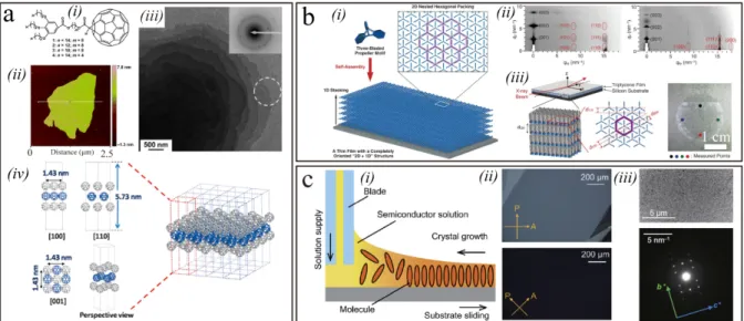
Thermotropic liquid crystals undergo phase transition into the liquid-crystal phase as temperature is changed, being a prominent advantage for the rapid formation of highly organized structures. For example, Zhang et al. synthesized a series of thermotropic [60]fullerene supramolecular liquid crystals to grow 2D crystals.[95] The design strategy relies
on the modification of gallic ester moiety with three long aliphatic chains acting as soft groups onto fullerene, as a result the strong π-π interactions and phase separation would force the molecules self-organize into 2D layered crystals (Figure 5a, i). 2D crystals could be formed upon solvent evaporation from their corresponding dilute solutions and exhibited a micrometer sized 2D layer with the thickness of 5-6 nm (Figure 5a, ii). Transmission electron microscopy (TEM) images clearly demonstrated the lamellar growth mode, indicating the 2D nature of the crystals (Figure 5a, iii). The deduced molecular packing of molecules in the supramolecular liquid crystals with the hierarchical structure are illustrated in Figure 5a iv. Through reasonable molecular design liquid crystals can spontaneously undergo self-assembly forming exceptionally long-range order structure. For example, Seiki et al. recently reported a space-filling strategy based on specially designed liquid crystal molecules-paraffinic modified triptycene.[96] Triptycene is a propeller-shaped rigid molecule with three 120° oriented
phenylene rings, such space-filling design offers a large free volume and allows triptycene molecules to self-assemble into a 2D hexagonal structure by nested packing (Figure 5b, i). The soft paraffinic chain of triptycenes could ensure a certain degree of fluidity to the molecules and facilitate their reorganization into ordered 2D structure. Centimeter-sized molecular films with long-range 2D structure can be fabricated by vacuum evaporation, spin-coating, and cooling from the isotropic liquid of the triptycene. X-ray diffraction analysis and 2D GI-XRD further confirmed the long-range order of the evaporated triptycene films and revealed that triptycene molecules form a completely oriented 2D + 1D (layer stacking) structure (Figure 5b, ii and iii).
Alongside spontaneous molecular self-assembly, external forces such as shear force, capillary force, or gravity force can also be utilized to guide the evaporating rate of solution to realize large area highly ordered 2D crystals domains.[56,97-100] Recently, Takeya et al. successfully
demonstrated wafer-scaled monolayer (1L), bilayer (2L), and trilayer (3L) molecular single crystal films through optimization of the depositon temperature, shearing speed of the substrate, and the solution concentration.[101] In the continuous edge-casting technique
displayed in Figure 5c i, the solute precipitation rate is critically influenced by the amount of solvent evaporation which is vital to steer the growth of 2D crystalline domains.
Cross-15
polarized optical microscopy confirmed the single-crystalline nature of the films (Figure 5c, ii). When the crystal growth direction is parallel or perpendicular to the polarization angle, no images can be obtained, indicating that the high degree of order. Figure 5c iii exhibits the TEM images and SAED patterns confirming the single crystalline structure of the monolayer C8-DNBDT-NW film. By and large, this strategy provides an efficient way of growing 2D crystals of small organic molecules, where it is possible to control the molecular layer thickness as well as their size and crystallinity degree.
A rough conclusion could be drawn from these results that the traditional drop-casting self-assembly method to form 2D nanostructure on a rigid substrate requires complex molecular design to balance adjacent intermolecular interactions. As a major improvement, the surface assistant self-assembly technique like “solution epitaxy” provides an efficient and universal way to achieve uniform, large-area and high-quality 2D molecular crystals. Of course, external forces can work very effectively in guiding the growth of large area 2D crystalline film, but these methods require additional equipment and undoubtedly will increase the cost and difficulty of device fabrication. Indeed, the compromise between the quality/size of the 2D organic monolayer and the cost to achieve represents the main issue in this field.
Figure 5. a) (i) Molecular structure of fullerene dyads. (ii) The AFM image of 2D crystals
formed by dyad. (iii) TEM image of 2D crystals. Inset: SAED pattern from selected monolayer 2D crystals. (iv) Representation of molecular packing of fullerene dyad into 2D crystals. Panel (a) Reproduced with permission.[95] Copyright 2015, Wiley-VCH. b) (i) Space-filling model
with a three-bladed, propeller-shaped motif, capable of forming a 2D hexagonal array by the interpenetration of its propeller parts. (ii) 2D GI-XRD characterization of the evaporated films
16
of Trip-C12 before and after annealing. (iii) Schematic representations of the experimental setup for GI-XRD and the assembly structure of a Trip-C12 film on a substrate. Panel (b) Reproduced with permission.[96] Copyright 2015, Science. c) (i) Schematic image of the
continuous crystal growth method. (ii) Cross-polarized optical microscopy images of the fabricated ultrathin C8-DNBDT-NW single crystals. (iii) TEM images and corresponding SAED patterns for 1L single crystal. Panel (c) Reproduced with permission.[101] Copyright
2018, Science.
Compared with bulk materials, the use of 2D molecular film as electroactive material in the channel would enable the metal electrodes to form direct contact with the accumulation layer, making it possible to improve the efficiency of carrier injection and modulation, thus greatly improving the performance of OFETs.[102,103] Furthermore, monolayer or few-layers thick
semiconductors could effectively eliminate interlayer screening, thereby offering an ideal system to directly probe the effect of disorder and the role of interfaces on charge transport.[104]
Jiang et al. successfully prepared large-area monolayer molecular crystals on polymer substrates.[94] Well-packed and quasi free-standing dicyanomethylene-substituted fused
tetrathienoquinoid (CMUT) molecular layer was obtained on the substrates without the need of an embedded interfacial layer. Typical 2D monolayer FETs on BCB/SiO2 showed electron
mobility of 0.51 cm2 V-1 s-1 and 0.52 cm2 V-1 s-1 as determined in saturated and linear regime.
Also, the mobility is almost independent from the gate voltage when Vg goes beyond the
threshold voltage (Vth), as revealed in Figure 6a i, indicating that the contact resistance and
interface traps have no effect on device performance. As portrayed in Figure 6a ii and iii, both the electron mobility and the corresponding source-drain current only exhibit minor variations with the decreasing channel length, which further confirms the superior quality of the monolayer crystals. Devices based on both SiO2/Si and BCB/SiO2 substrates were then
measured at different temperatures: the temperature dependence of current-voltage curves and the mobility are displayed in Figure 6a iv. The monolayer devices based on the BCB/SiO2
substrate exhibited a band-like transport characteristic, with the mobility decreasing upon temperature increase from 200 to 300 K. In comparison, no band-like behavior was observed in the devices fabricated on SiO2 substrates. This difference may be caused by two factors: (i)
17
SiO2/monolayer interface, (ii) the smaller dielectric constant of BCB (2.6) when compared to
SiO2 (3.9) can yield a lower dipole-induced disorder.
When top contact geometries are used in organic thin-film transistors, the charge carriers need to move through high resistance organic layer in the out-of-plane direction to reach the conduction channel. In theory the net contact resistance can be significantly reduced when the thickness of organic layer is reduced. To cast light onto the relationship between the thickness of organic layer and resistance, the gated four-point probe (gFPP) method was used to evaluate the bilayer (2L) and trilayer (3L) OFETs (Figure 6b, i).[101] In the bilayer OFET, the drain
current (ID) is proportional to ∆Vcs (∆Vcs is the voltage drop at each source electrode), which
demonstrates that ohmic contact is formed (Figure 6b, ii). On the other hand, the trilayer OFET showed a super linear dependence in ID-∆Vcs; in particular, the super linearity is more obvious
in the lower ∆Vcs region (Figure 6b, iii), which indicates the multilayered OFETs are likely to
work under a Schottky barrier. Transistors with different channel lengths were fabricated for bilayer and trilayer crystalline films to analyze the contact resistance (RC) qualitatively, by
extracting them using the transmission line method. The RC·W of the 2L-OFET was found to
be 5 times smaller than in 3L device, as displayed in Figure 6b iv. This result provided evidence that the contact resistance in top-contact devices can be considerably lowered by decreasing the film thickness.
Figure 6. a) Electrical properties of monolayer molecular crystals FETs: (i) Mobility as a
function of Vg at Vds=30 V. (ii) Electron mobility and drain current of the 2D monolayer FETs
at different channel lengths on BCB/SiO2. (iii) Contact resistance of monolayer (red sphere)
18
Temperature-mobility relationship of the monolayer on SiO2 (red sphere) and BCB/SiO2 (blue
triangle). Panel (a) Reproduced with permission.[94] Copyright 2018, Nature Publishing Group.
b) (i) Schematic illustration of the gFPP measurement. Voltage drops at the source and drain electrodes are estimated by extrapolation of the potential profile. (ii-iii) Relationship between ∆Vcs and the drain current measured by gFPP for the (ii) 2L-OFET and (iii) 3L-OFETs; (iv)
Contact resistance and the gate voltage relationship for the 2L- and 3L-OFETs. Panel (b) Reproduced with permission.[101] Copyright 2018, Science.
3. Lithography techniques for the nanofabrication of electrodes
The optimal high-density integration of supramolecular nanostructures in high-performance devices, and eventually in circuitries, requires the use of micro- and nano-fabrication protocols.[105-107] However, the wiring-up of nanoscale supramolecular assemblies with
structurally and energetically well-defined electrodes is a major scientific challenge. This is due to the fragility of these non-covalent architectures. In particular, the limited stability to exposure at high temperature or to organic solvent, renders these nanostructures poorly compatible with typical top-down photolithography techniques that typically involve solvent treatment. In earlier works, electrodes were directly fabricated by manually painting conductive glue onto the crystals. Of course, this coarse method may cause mechanical damage and it is not particularly suited for micro/nano devices fabrication.[108-110] So far, various
unconventional and non-destructive procedures have been developed (Figure 7 and Figure 8) to fabricate devices based on self-assembled nanostructures with bottom- or top-contact configuration.
3.1 Shadow mask lithography and stamping technique
During vacuum evaporation of top electrodes, a copper grid or an organic ribbon could serve as shadow mask to spatially confine the deposition of the metallic electrode in order to wire-up individual swire-upramolecular nanostructures, as illustrated in Figure 7a i.[64,111-114] When using
as a mask organic wires/ribbons, the latter can be electrostatically bonded onto the probe tip of the micro-manipulation system which can be moved precisely, thus enabling displacement at demand (Figure 7a, i). Moreover, this technique can eliminate the mechanical damage which can occur when employing other shadow masks, thanks to the mechanical flexibility of the
19
organic wires/ribbons and their electrostatic bonding effect with the probe tip. The copper grid mask and organic ribbon mask provide efficient way for fabricating devices with small dimensions. For example, the channel length can also be narrowed down to < 1 μm by rational optimization.[115] If the electrode materials are changed during the second deposition,
asymmetric electrodes can be obtained by simply changing the relative position between the sample and the metal source, because the oblique incidence of metal vapor can be achieved leading to deposition of the electrodes beneath the mask near its edge.[111] This oblique
incidence provides an effective way to fabricate asymmetric electrodes and it is instrumental for the generation of stepwise energy levels among the drain electrode, the supramolecular structures and the source electrode. Similarly, different types of shadow masks have been used to provide a shadow effect, such as gold wires or plastic fiber.[115-118]
In general, top-contact configuration could ensure better charge injection and devices performance, whereas bottom-contact configuration is adopted when nanostructures are unstable in vacuum or top electrode deposition too complicated. It should be noted that commercial metal pre-patterned metallic dielectric substrates for bottom-contact configuration provide easy access to integrated electrodes with channel lengths starting from 2 µm, whereas the deposition of similarly small interelectrodic gaps for top-contact solutions is not easy, despite top-contact guarantees a better connection between electrodes and supramolecular nanostructures. Moreover, top-contact devices require the thermal evaporation of electrodes on the organic supramolecular nanostructures. Such a thermal shock might disrupt the inner structure of organic semiconductors and cause contact issues at electrode/semiconductor interface. In order to circumvent thermal radiation damage and the filling of pinholes in the dielectric layer by metal atoms during electrode vacuum deposition, Hu and co-workers explored a mechanical technique to paste electrodes onto crystals directly.[112,119,120] This
process is presented in Figure 7a ii. Specifically, a small piece of pre-patterned coinage metal is transferred from a wafer surface to the micromanipulator probe, then such a metal piece is placed onto the crystals directly to form the drain/source electrodes. The thickness of the electrode film is about 100 nm, which is dependent on the scalability and ductility of the materials.[121] It should be mentioned that channel lengths with several micrometers can be
obtained by using this protocol, which can meet the challenge of fabricating micro/nano devices. Additionally, this procedure can also provide asymmetric drain/source electrodes by stamping two different electrode strips (e.g., gold and silver film) as the drain and source electrodes respectively (Figure 7a, ii).[122] The “cold” electrode technique circumvents the
20
disadvantages of thermal evaporation and thus ensures high device performance. Furthermore, this technique needs only modest infrastructures, hence it is very appropriate for the fundamental study of organic supramolecular nanostructures. This method also can be applied to a variety of metals with different work functions to meet the needs of different energy levels for harvesting some unique properties of organic semiconductors (e.g. ambipolarity, etc). As we mentioned above, the organic ribbon and “cold” stamping techniques could enable in-situ and non-destructive wiring-up of “small” crystals to form nanodevices. However, the manual manipulation is unsuitable for the processing of complex multicomponent devices and batch production toward commercial products. Recently, Lee et al. reported a novel large-area organic nanowire lithography (ONWL) by using the electrospinning method to fabricate defined electrodes (Figure 7b, i).[123] The high-speed electrohydrodynamic organic nanowire
printer can controllably and precisely print large-area high-quality organic semiconducting nanowire arrays onto arbitary substrates. It also enables sophisticated large-area nanowire lithography for nano-electronics, by scaling down channel lengths to 100 nm (Figure 7b, ii and iii). The ONWL can print, align and pattern circular organic nanowires in arbitrary positions and orientations directly onto large-area substrate. This technique represents a promising approach to realize large-area flexible nano-electronic and practical electronics applications.
Figure 7. a) (i) Schematic diagrams of the fabrication procedure for deposition of drain/source
electrodes by using the shadow mask technique (copper grid or organic ribbon as the mask). (ii) Schematic diagrams of a fabrication procedure for deposition of symmetric (top) and asymmetric (bottom) drain/source electrodes through a “stamping” technique by transferring the pre-deposited metal films onto the mciro/nano crystals. Panel (a, i) Reproduced with
21
permission.[111] Copyright 2010, American Chemical Society. Panel (a, ii) Reproduced with
permission.[120] Copyright 2011, Royal Society of Chemistry. b) (i) Schematic diagram of
organic nanowire printer and nanowire printing process. (ii) Schematic illustration of the process for organic nanowire lithography (ONWL). (iii) Schematic illustration (left) and scanning electron microscope image (right) showing the cross-section of organic nanowires after metal deposition process in ONWL. Panel (b) Reproduced with permission.[123] Copyright
2013 Nature Publishing Group.
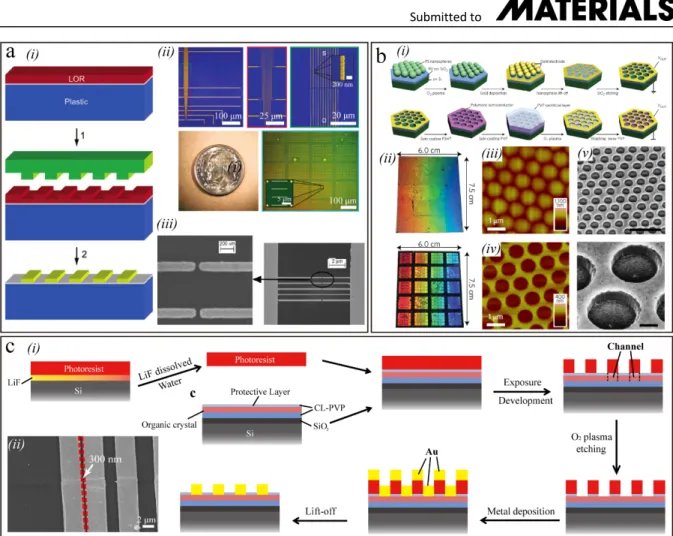
3.2 Nanoimprint lithography
Nanoimprint lithography (NIL) is another unconventional and low-cost high-resolution patterning method for the reproducible wiring-up of polymer nanostructures with excellent precision.[124-126] In contrast to traditional photolithography, NIL does not need the use of
electromagnetic or electronic fields to change the chemical and physical properties of the photoresist. NIL relies on direct mechanical deformation of the polymer material by using a hard inorganic stamp, so that it can break through the limitations defined by light diffraction and achieve even a high-resolution of tens of nanometres. Alhough NIL was demonstrated being very successful in transfering nanoscale structures, it suffers from the same constraints of a traditional lithography technique. Its fundamental molding characteristics (i.e., physically displacing polymer materials) frequently cause pattern defects when transfering high-resolution patterns, especially for patterns with wide size distribution. To solve this problem, Lieber et al. developed a general nanoimprint lithography for high definition electrodes, as shown in Figure 8a i.[127] First, the lift-off resist was spread over a SiO
2 layer supported on the
plastic substrate. Second, the resist was imprinted by using Si/SiO2 stamps. In general, these
stamps can be reused several times without significant loss of resolution. Finally, the patterned resist was etched to the SiO2 layer using reactive ion etching, and metal electrodes were
deposited by thermal evaporation. The results demonstrate that NIL is capable of uniformly patterning metal electrode over millimeter scale with hundred nanometers resolution (Figure 8a, ii). After that, Guo et al. have developed a novel method by combining nanoimprint and classic photolithography that uses a hybrid mask to obtain much higher resolution, thereby reaching channel lengths between the fabricated nanoelectrode from 150 μm down to tens of nanometers (Figure 8a, iii).[128] With combined advantages of both techniques, this method
22
offers a technological solution for low-cost, mass production of micro/nanoscale patterns and devices.
3.3 Colloidal lithography
Nanosphere lithography, which relies on the formation and use of a hexagonal closely-packed nanosphere monolayer serving as a soft mask, is a highly efficient method for fabricating large-area patterned functional nanostructures.[129,130] The nanosphere lithography based on
self-assembled colloidal spheres provides a efficient way for obtaining highly periodic nanostructures with the advantages of low-cost, high-throughput and simple processing.[131] By
controlling experimental parameters and materials, colloidal lithography represents a promising method for fabricating large-area and periodic nanostructures onto various materials like metals, graphene, organic semiconductors, etc.[132-134] Recently, we reported a novel highly
integrated vertical-channel hexagonal nanomesh scaffold featuring asymmetric (nano)electrodes by using the colloidal lithography (Figure 8b).[42] A polystyrene (PS)
nanosphere (800-1000 nm) monolayer was firstly transferred onto substrate (Figure 8b, i). Then oxygen plasma treatment was used to partially etch closely packed PS nanospheres and make gaps between adjacent nanospheres. Before a lift-off process, gold is deposited through thermal evaporation. At last, the Au nanomesh scaffold acts as a mask to selectively etch the SiO2
dielectric layer through reactive ion etching. The electrode distance in the device is determined by the thickness of the dielectric layer. This fabrication process demonstrated impressive consistency and high success rate (nearly 83%). More importantly, the nanohole can be filled with different kinds of semiconducting polymer to meet different application requirements (Figure 8b, i). Figure 8b ii shows images of the closely packed PS nanosphere monolayer and the corresponding nanomesh, respectively. The AFM images of samples displayed in Figure 8b iii and iv respectively. The colorful appearance in the photographs suggest that the PS nanosphere monolayers and honeycomb-like nanomesh scaffold formed a highly periodic nanostructure. The SEM images further confirm that the gold nanomesh closely attach to the SiO2 layer without any collapsing (Figure 8b, v).
3.4 Direct Photolithography
For supramolecular organic nanocrystals most sophisticated patterning technologies such as e-beam lithography or focused-ion-e-beam (FIB) cannot be directly applied on organic crystals because the organic nanostructures are very sensitive to the electron beam and heat.[49,111]
23
Photolithography is a general protocol to pattern parts of a thin film or the bulk of a sample. It uses light to transfer of geometric shapes on a mask to a light-sensitive photoresist on the substrate. Although photolithography has been widely exploited and constructed the foundation of modern silicon microelectronics, extending direct photolithography onto microscopic organic crystals or supramolecular nanostructures is extremely challenging. For example, the fragile molecular crystals are not tolerant to the solvents of photoresist and alkaline developer. The brittle nature of molecular crystals which does not allow them to undergo through the photoresist lift-off process safely. Recently, we have reported a novel technique to enable the direct photolithography to compatible with molecular crystals, with a spatial resolution below 300 nm, thereby allowing simultaneous integrating of multiple crystals to realize various complicated application.[135] The process of the direct photolithography
technique is shown in Figure 8c i. The most important steps in this technique are using water-flotation method to transfer photoresist film onto target substrate and lift-off in ethanol which is an antisolvent for most organic semiconducting materials. The SEM images of the patterned gold electrodes in Figure 8c ii demonstrated that the channel length in the device bearing the PDI-C8 microwire can be down to ∼300 nm, which is one of the best results for the top-contact OFETs.[115,123] The versatility of direct photolithography technique allows integrating multiple
discrete organic nanostructures at the same time and the channel length of the devices to be further designed from hundreds of nanometers up to hundreds of micrometers.
24
Figure 8. a) (i) Schematic of the nanoimprint process on plastic substrates. (ii) Optical image
of source/drain electrodes array and interconnect wires. (iii) SEM micrographs of a finger-shaped nanoelectrode. Panel (a, i and ii) Reproduced with permission.[127] Copyright 2003,
American Chemical Society. Panel (a, iii) Reproduced with permission.[128] Copyright 2006,
Institute of Physics Publishing. b) (i) Preparation process for the nanomesh scaffold through colloidal lithography. (ii) Pictures of a large-area PS nanosphere monolayer (top) and the nanomesh electrodes (bottom) on the silicon substrate. (iii-iv) AFM image of the PS nanosphere monolayer and final nanomesh scaffold. (v) SEM image of the fabricated nanomesh electrodes (top: scale bars 2 μm; bottom: scale bars 200 nm). Panel (b) Reproduced with permission.[42] Copyright 2016, Nature Publishing Group. c) (i) Schematic diagram of the
direct photolithography technique. (ii) SEM image of patterned electrodes, the channel length is around 300 nm. Panel (c) Reproduced with permission.[135] Copyright 2018, American
Chemical Society.
25
Self-assembled semiconducting supramolecular nanostructures are promising platforms which can combine the advantages of soft materials such as polymers regarding flexibility and solution processability with the higher degree of order of organic crystals.[136-139] The high
crystallinity of the assemblies and the intrinsic optimal intermolecular overlapping of their π-conjugated clouds, guarantee efficient transport of the charge carriers along these semiconducting supramolecular nanostructures to reach the electrodes.[140-143] Thanks to their
high absorption coefficient and outstanding light sensitivity concerning their bulk counterpart, supramolecular organic nanowires (SMNWs) are ideal choice for application in nano-optoelectronics owing to their efficient exciton generation and transport properties.[144,145]
However, previous works on supramolecular electronics focus mainly on the design of novel low-dimensional materials from a chemical standpoint, and less attention has been paid on the integration of brittle and fragile supramolecular assemblies into macroscopic optoelectronic devices. Such a constraint has hindered the further development of the field of supramolecular electronics. In recent years, we have conducted a series of studies on this topic, which led to the emergence of a series of strategies to surpass this barrier by devising different nanofabrication technology and supramolecular device architectures.
4.1 Photovoltaic devices on molecular crystals
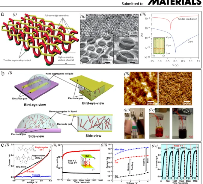
Organic molecular crystals featuring long-range order and compact π-π stacking are unique materials for efficient exciton and charge transport. For example, the triplet exciton diffusion length in rubrene crystals could occur over macroscopic distances (2-8 μm), which is comparable to the light absorption length.[146] High-quality organic molecular crystals are
therefore promising candidates for applications in optoelectronics. However, these highly crystalline but discrete organic semiconductors are rarely considered for practical applications in photovoltaics, because the difficulties of selectively connecting the two kinds of crystals (p- and n-type) with cathode and anode, and simultaneously wire-up hundreds of discrete crystals p-n junctions cost-effectively. By use of the vertical nanomesh scaffold, Zhang et al. defined a general approach to connect multiple crystals heterojunctions with asymmetric nanoelectrodes selectively.[31] In detail, we successfully introduced n-type
N,N′-Dioctyl-3,4,9,10-perylenedicarboximide (PDI-C8) and p-type 6,13-bis(triisopropylsilylethynyl)pentacene (TIPS-PEN) as bi-crystals heterojunctions into the vertical-yet-open asymmetric architecture. The bi-crystals heterojunctions nanomesh scaffold photovoltaic devices are shown as Figure
26
9a i. The existence of rigid SiO2 sidewall between neighbouring cells inhibits formation of
crystalline domains extended over larger scales. The optical microscopy image in Figure 9a ii, shows PDI nanowires and elongated TIPS-PEN microplates are closely stacked on the device surface. The presence of birefringence, as demonstrated by linearly polarized microscopy images in Figure 9a ii, suggests the bi-crystal nature of PDI-C8 and TIPS-PEN. We also observed distinct photovoltaic effect through these bi-crystals heterojunctions which are asymmetrically integrated into the external circuit with the open circuit voltage (VOC) around
0.35-0.40 V and slightly changed by irradiation wavelength. The crystal-based photonic device showed a remarkable signal-to-noise ratio of 107 as a self-powered photodetector. More
importantly, vertical-yet-open device configuration shares the advantages of short interelectrodic distance (approx. 120 nm), and the short electrode-to-electrode distance will result in an ultrafast photoresponse compared to the photodetectors in a lateral configuration. The photonic device showed an ultra-fast photoresponse time less than 100 ns at different wavelength in both photovoltaic and photoconduction mode, as shown in Figure 9a iii. The introduction of bi-crystal heterojunction demonstrated the vertical-yet-open asymmetric architecture is also suitable to construct diverse p-n organic crystals as long as they are grown using orthogonal solvents.
Taking this step further, Zhang et al. recently demonstrated the self-suspended nanomesh scaffold is compatible with rigid glass and flexible plastic substrates, making it possible to selectively integrate p-n crystal heterojunctions into high-performance photovoltaic devices.[147] In this report, the crosslinked poly(4-vinylphenol) (CL-PVP) is used as the
insulator layer because of its robust dielectric property and solvent resistance. Different from SiO2, a hollow nanomesh scaffold can be achieved when using CL-PVP as the dielectric layer
by controlling the duration of the oxygen plasma treatment. This unique hollow structure could get rid of physical barriers to the growth of crystalline domains and highly beneficial to connect adjacent regions to realize a large-area self-suspended nanomesh electrode.[148,149] Figure 9b i
shows the picture of bent self-supported nanomesh scaffold devices on PET substrate, after 1000 times bending fatigue test the photoresponsivity slightly reduced to 79% of its initial performance, but the structural strength of hollow nanomesh scaffold was solid enough to maintain a ultralow leakage current through the whole bending test (Figure 9b, ii and iii). Figure 9b iv shows the I-V curves of the flexible crystalline photovoltaic device under different wavelength. The signal-to-noise ratio could reach up to 105 in the photovoltaic mode.
27
showed an ultra-fast photoresponse time of 8 ns (Figure 9b v). By means of the hollow nanomesh scaffold, TIPS-PEN could form large-area high-quality crystalline domains below PDI-C8 crystalline nanowires resulting high-quality p-n heterojunctions, which effectively facilitate exciton separation and transportation.
Direct photolithography can directly connect multiple molecular crystals simultaneously into micro-/nano-devices. This technique is compatible with both rigid silicon substrate and flexible plastic substrates such as polyethylene terephthalate (PET). At this point, as a proof-of-concept Yao et al. have successfully constructed OFETs and complementary inverter, based on p-type 2,7-diphenyl[1]benzothieno[3,2-b][1]-benzothiophene (Dph-BTBT) nanoflakes and n-type PDI-C8 nanowires, supported on PET foils with typical switching characteristic, and a gain of ~7 (Figure 9c, ii). 3D schematic diagrams of the inverter as shown in Figure 9c i.[135] The direct
photolithography technique provides a valuable tool for investigating the inherent photonic properties of one-dimensional semiconducting materials. We have fabricated crystalline donor-acceptor heterojunction photovoltaic devices with planar geometry and asymmetric Au-Ag electrodes (Figure 9c, i). With these crystalline heterojunctions prototypical device, we have explicitly illustrated energy level effects on short-circuit current and open-circuit voltage and realized large open-circuit voltage modulation from 0.56 V to 1.4 V when the irradiation wavelength is changed from 320 to 690 nm, which is originated from energy level mismatch (Figure 9c, iii). The possibility of extending photolithography to organic semiconducting crystals permits to fully study their intrinsic properties by precisely constructing patterned electrodes on their top to finally combine inorganic and organic crystals towards high-performance hybrid (opto)electronic solutions.
28
Figure 9. a) (i) Cartoon illustration of a multiple bi-crystals photovoltaic devices sustained by
the nanomesh. (ii) Birefringence of PDI-C8 nanowires (red) and TIPS-PEN microplates (blue) as verified by polarized optical microscopy. The inset shows an optical microscopy image. (iii) Photocurrent as a function of time for the identical device in photoconduction (1.5 V bias) and photovoltaic (0 V bias) modes, respectively. Panel (a) Reproduced with permission.[31]
Copyright 2017, Wiley-VCH. b) (i) The self-suspended nanomesh scaffold devices were bent over a cylinder with a radius of 1 cm for ~1000 times. (ii) After 1000 times bending fatigue test, the device showing the same photoresponsivity spectrum, but the absolute value reduced by 21%. (iii) Ultralow leakage current after 1000 times bending fatigue test. (iv) Dark and light I-V curves of the flexible organic crystalline photovoltaic device. (v) The transient photocurrent measurement after irradiating the device with a 3 ns green laser pulse. Panel (b) Reproduced with permission.[147] Copyright 2018, Wiley-VCH. c) (i) 3D schematic diagram of
a CMOS inverter and crystalline heterojunction photovoltaic device based on PDI-C8 and Dph-BTBT crystals. (ii) Output voltage as a function of input voltage when the device was driven by 60V VDD. The inset shows the gain of the inverter. (iii) J-V curves of the heterojunction
open-29
circuit voltage significantly shifts from 0.56 to 1.4 V when the illumination wavelength changes from 320 to 690 nm. Panel (c) Reproduced with permission.[135] Copyright 2018,
American Chemical Society.
4.2 Wiring-up asymmetric supramolecular organic nanowires and gels
Supramolecular nanostructures are particularly appropriate for exciton dissociation and transport because their ordered molecular packing and high surface-to-bulk ratio minimizes the diffusion length from the interior to the interface where exciton separation typically occurs. [150-153] Recently, long-range exciton transport, up to a few micrometers, a distance that is limited
only by the fiber length, has been reported in single supramolecular nanofibers.[144] Other
advantages for photonic applications include a lower interface reflection loss compared with bulks and the possibility of tuning the optoelectronic properties by rational molecular design and aggregation.[154,155] All of these unique features make supramolecular nanostructures
become ideal choices for organic optoelectronic devices.
Recently, we described a general approach to integrating multiple supramolecular nanowires into a novel hexagonal nanomesh scaffold featuring asymmetric (nano)electrodes to realize photovoltaic cell.[42] Device configuration as shown in Figure 10a i, flexible PDI-C8 nanowires
produced through SIP was incorporate 3D hollow asymmetrical nanomesh scaffold. Figure 10a ii displays the SEM images large-area supramolecular nanowires supported on top of a nanomesh scaffold. It shows that almost every nanohole bears nanowires as further proved by the zoom-in SEM images. To improve the photovoltaic device performance, improve hole selectivity and suppress non-radiative recombination at the Si/nanowire interface, the nanohole could be filled with various kinds of p-type semiconducting polymers thereby forming a p-n junction with the PDI-C8 nanowires. Figure 10a iii displays typical current-voltage (I-V) curves of PDI-C8 supramolecular nanowires on a P3HT-modified nanomesh scaffold. Photovoltaic effect was successfully observed with 0.3 V open-circuit voltage, that could be attributed to effective light absorption and exciton separation at the PDI-C8/P3HT interface. After anode modification with P3HT, the signal-to-noise ratio of PDI-C8 supramolecular nanowire devices increased up to as much as 107 in the photovoltaic mode. Moreover, the
photoresponse time as fast as 10 ns and an external quantum efficiency exceeding 50%. The nanomesh scaffold structure represents a valuable tool for investigating inherent photonic properties of self-assembly one-dimensional semiconducting materials. In the vertical